

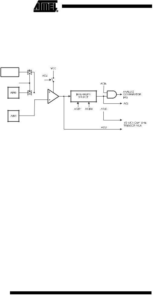
Analog Comparator The Analog Comparator compares the input values on the positive pin AIN0 and negative pin AIN1. When the voltage on the positive pin AIN0 is higher than the voltage on the negative pin AIN1, the Analog Comparator Output, ACO, is set. The comparator’s output can be set to trigger the Timer/Counter1 Input Capture function. In addition, the comparator can trigger a separate interrupt, exclusive to the Analog Comparator. The user can select Interrupt triggering on comparator output rise, fall or toggle. A block diagram of the comparator and its surrounding logic is shown in Figure 71.
Figure 71. Analog Comparator Block Diagram(1)
BANDGAP
REFERENCE
ACBG
Note: 1. Refer to Figure 1 on page 2 and Table 29 on page 66 for Analog Comparator pin placement.
Analog Comparator Control
and Status Register – ACSR
Bit |
7 |
6 |
5 |
4 |
3 |
2 |
1 |
0 |
|
|
ACD |
ACBG |
ACO |
ACI |
ACIE |
ACIC |
ACIS1 |
ACIS0 |
ACSR |
|
|
|
|
|
|
|
|
|
|
Read/Write |
R/W |
R/W |
R |
R/W |
R/W |
R/W |
R/W |
R/W |
|
Initial Value |
0 |
0 |
N/A |
0 |
0 |
0 |
0 |
0 |
|
• Bit 7 – ACD: Analog Comparator Disable
When this bit is written a logic one, the power to the Analog Comparator is switched off. This bit can be set at any time to turn off the Analog Comparator. This will reduce power consumption in Active and Idle mode. When changing the ACD bit, the Analog Comparator Interrupt must be disabled by clearing the ACIE bit in ACSR. Otherwise an interrupt can occur when the bit is changed.
• Bit 6 – ACBG: Analog Comparator Bandgap Select
When this bit is set, a fixed bandgap reference voltage replaces the positive input to the
Analog Comparator. When this bit is cleared, AIN0 is applied to the positive input of the
Analog Comparator. See “Internal Voltage Reference” on page 49.
• Bit 5 – ACO: Analog Comparator Output
The output of the Analog Comparator is synchronized and then directly connected to
ACO. The synchronization introduces a delay of 1 - 2 clock cycles.
• Bit 4 – ACI: Analog Comparator Interrupt Flag
This bit is set by hardware when a comparator output event triggers the interrupt mode defined by ACIS1 and ACIS0. The Analog Comparator Interrupt routine is executed if the ACIE bit is set and the I-bit in SREG is set. ACI is cleared by hardware when executing the corresponding interrupt handling vector. Alternatively, ACI is cleared by writing a logic one to the flag.
162 ATmega8515(L)
2512G–AVR–03/05

 ATmega8515(L)
• Bit 3 – ACIE: Analog Comparator Interrupt Enable
When the ACIE bit is written logic one and the I-bit in the Status Register is set, the Analog Comparator interrupt is activated. When written logic zero, the interrupt is disabled.
• Bit 2 – ACIC: Analog Comparator Input Capture Enable
When written logic one, this bit enables the Input Capture function in Timer/Counter1 to be triggered by the Analog Comparator. The comparator output is in this case directly connected to the Input Capture front-end logic, making the comparator utilize the noise canceler and edge select features of the Timer/Counter1 Input Capture interrupt. When written logic zero, no connection between the Analog Comparator and the Input Capture function exists. To make the comparator trigger the Timer/Counter1 Input Capture interrupt, the TICIE1 bit in the Timer Interrupt Mask Register (TIMSK) must be set.
• Bits 1, 0 – ACIS1, ACIS0: Analog Comparator Interrupt Mode Select
These bits determine which comparator events that trigger the Analog Comparator interrupt. The different settings are shown in Table 72.
Table 72. |
ACIS1/ACIS0 Settings |
||
ACIS1 |
|
ACIS0 |
Interrupt Mode |
|
|
|
|
0 |
|
0 |
Comparator Interrupt on Output Toggle |
|
|
|
|
0 |
|
1 |
Reserved |
|
|
|
|
1 |
|
0 |
Comparator Interrupt on Falling Output Edge |
|
|
|
|
1 |
|
1 |
Comparator Interrupt on Rising Output Edge |
|
|
|
|
When changing the ACIS1/ACIS0 bits, the Analog Comparator interrupt must be disabled by clearing its Interrupt Enable bit in the ACSR Register. Otherwise an interrupt can occur when the bits are changed.
163
2512G–AVR–03/05

Boot Loader Support
– Read-While-Write
Self-Programming
The Boot Loader Support provides a real Read-While-Write Self-Programming mechanism for downloading and uploading program code by the MCU itself. This feature allows flexible application software updates controlled by the MCU using a Flash-resi- dent Boot Loader program. The Boot Loader program can use any available data interface and associated protocol to read code and write (program) that code into the Flash memory, or read the code from the Program memory. The program code within the Boot Loader section has the capability to write into the entire Flash, including the Boot Loader memory. The Boot Loader can thus even modify itself, and it can also erase itself from the code if the feature is not needed anymore. The size of the Boot Loader memory is configurable with fuses and the Boot Loader has two separate sets of Boot Lock bits which can be set independently. This gives the user a unique flexibility to select different levels of protection.
Features |
• |
Read-While-Write Self-Programming |
|
• |
Flexible Boot Memory Size |
|
• |
High Security (Separate Boot Lock bits for a Flexible Protection) |
|
• |
Separate Fuse to Select Reset Vector |
|
• |
Optimized Page(1) Size |
|
• |
Code Efficient Algorithm |
|
• |
Efficient Read-Modify-Write Support |
Note: 1. A page is a section in the Flash consisting of several bytes (see Table 89 on page 181) used during programming. The page organization does not affect normal operation.
Application and Boot
Loader Flash Sections
Application Section
The Flash memory is organized in two main sections, the Application section and the Boot Loader section (see Figure 73). The size of the different sections is configured by the BOOTSZ Fuses as shown in Table 78 on page 175 and Figure 73. These two sections can have different level of protection since they have different sets of Lock bits.
The Application section is the section of the Flash that is used for storing the application code. The protection level for the Application section can be selected by the application Boot Lock bits (Boot Lock bits 0), see Table 74 on page 167. The Application section can never store any Boot Loader code since the SPM instruction is disabled when executed from the Application section.
BLS – Boot Loader Section While the Application section is used for storing the application code, the Boot Loader software must be located in the BLS since the SPM instruction can initiate a programming when executing from the BLS only. The SPM instruction can access the entire Flash, including the BLS itself. The protection level for the Boot Loader section can be selected by the Boot Loader Lock bits (Boot Lock bits 1), see Table 75 on page 167.
Read-While-Write and No
Read-While-Write Flash
Sections
Whether the CPU supports Read-While-Write or if the CPU is halted during a Boot Loader software update is dependent on which address that is being programmed. In addition to the two sections that are configurable by the BOOTSZ Fuses as described above, the Flash is also divided into two fixed sections, the Read-While-Write (RWW) section and the No Read-While-Write (NRWW) section. The limit between the RWWand NRWW sections is given in Table 79 on page 175 and Figure 73 on page 166. The main difference between the two sections is:
•When erasing or writing a page located inside the RWW section, the NRWW section can be read during the operation.
•When erasing or writing a page located inside the NRWW section, the CPU is halted during the entire operation.
164 ATmega8515(L)
2512G–AVR–03/05
ATmega8515(L)
Note that the user software can never read any code that is located inside the RWW section during a Boot Loader software operation. The syntax “Read-While-Write section” refers to which section that is being programmed (erased or written), not which section that actually is being read during a Boot Loader software update.
RWW – Read-While-Write If a Boot Loader software update is programming a page inside the RWW section, it is Section possible to read code from the Flash, but only code that is located in the NRWW section. During an on-going programming, the software must ensure that the RWW section never is being read. If the user software is trying to read code that is located inside the RWW section (i.e., by a rcall/rjmp/lpm or an interrupt) during programming, the software might end up in an unknown state. To avoid this, the interrupts should either be disabled or moved to the Boot Loader section. The Boot Loader section is always located in the NRWW section. The RWW Section Busy bit (RWWSB) in the Store Program memory Control Register (SPMCR) will be read as logical one as long as the RWW section is blocked for reading. After a programming is completed, the RWWSB must be cleared by software before reading code located in the RWW section. See “Store Program memory
Control Register – SPMCR” on page 168. for details on how to clear RWWSB.
NRWW – No Read-While-Write The code located in the NRWW section can be read when the Boot Loader software is Section updating a page in the RWW section. When the Boot Loader code updates the NRWW
section, the CPU is halted during the entire page erase or page write operation.
Table 73. Read-While-Write Features
Which Section does the Z- |
Which Section Can be |
|
Read-While- |
pointer Address during the |
Read during |
Is the CPU |
Write |
Programming? |
Programming? |
Halted? |
Supported? |
|
|
|
|
RWW section |
NRWW section |
No |
Yes |
|
|
|
|
NRWW section |
None |
Yes |
No |
|
|
|
|
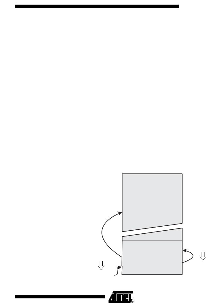
Figure 72. Read-While-Write vs. No Read-While-Write
Read-While-Write
(RWW) Section
|
Z-pointer |
|
Addresses NRWW |
Z-pointer |
Section |
|
|
Addresses RWW |
No Read-While-Write |
Section |
(NRWW) Section |
|
CPU is Halted |
Code Located in |
during the Operation |
|
|
NRWW Section |
|
Can be Read during |
|
the Operation |
|
165
2512G–AVR–03/05