


16-bit Timer/Counter1
Overview
The 16-bit Timer/Counter unit allows accurate program execution timing (event management), wave generation, and signal timing measurement. The main features are:
•True 16-bit Design (i.e., allows 16-bit PWM)
•Two Independent Output Compare Units
•Double Buffered Output Compare Registers
•One Input Capture Unit
•Input Capture Noise Canceler
•Clear Timer on Compare Match (Auto Reload)
•Glitch-free, Phase Correct Pulse Width Modulator (PWM)
•Variable PWM Period
•Frequency Generator
•External Event Counter
•Four Independent Interrupt Sources (TOV1, OCF1A, OCF1B, and ICF1)
Most register and bit references in this section are written in general form. A lower case “n” replaces the Timer/Counter number, and a lower case “x” replaces the Output Compare unit channel. However, when using the register or bit defines in a program, the precise form must be used, i.e., TCNT1 for accessing Timer/Counter1 counter value and so on.
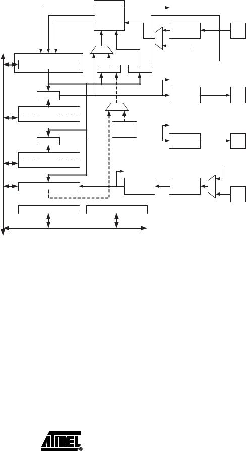
A simplified block diagram of the 16-bit Timer/Counter is shown in Figure 47. For the actual placement of I/O pins, refer to “Pin Configurations” on page 2. CPU accessible I/O Registers, including I/O bits and I/O pins, are shown in bold. The device-specific I/O Register and bit location are listed in the “16-bit Timer/Counter Register Description” on page 118.
96 ATmega8515(L)
2512G–AVR–03/05
 ATmega8515(L)
Figure 47. |
16-bit Timer/Counter Block Diagram(1) |
|
|
||
|
|
Count |
|
TOVn |
|
|
|
Clear |
|
(Int.Req.) |
|
|
|
Control Logic |
Clock Select |
|
|
|
|
Direction |
clkTn |
|
|
|
|
|
|
Edge |
Tn |
|
|
|
|
Detector |
|
|
|
|
|
|
|
|
|
TOP |
BOTTOM |
|
|
|
Timer/Counter |
|
|
( From Prescaler ) |
|
|
|
|
|
|
|
|
TCNTn |
= |
= 0 |
|
|
|
|
|
|
||
|
|
|
|
OCnA |
|
|
|
|
|
(Int.Req.) |
|
|
= |
|
|
Waveform |
OCnA |
|
|
|
Generation |
||
|
|
|
|
|
|
|
OCRnA |
|
|
|
|
|
|
|
Fixed |
OCnB |
|
|
|
|
(Int.Req.) |
|
|
BUS |
|
|
TOP |
|
|
= |
|
|
OCnB |
||
|
Values |
Waveform |
|||
|
|
|
|
|
|
DATA |
|
|
|
Generation |
|
OCRnB |
|
|
|
( From Analog |
|
|
|
|
|
|
|
|
|
|
|
|
Comparator Ouput ) |
|
|
|
ICFn (Int.Req.) |
|
|
|
ICRn |
|
Edge |
Noise |
|
|
|
Detector |
Canceler |
|
|
|
|
|
ICPn |
||
|
|
|
|
|
|
|
TCCRnA |
TCCRnB |
|
|
|
|
Note: 1. Refer to Figure 1 on page 2, Table 29 on page 66, and Table 35 on page 71 for |
||||
|
Timer/Counter1 pin placement and description. |
||||
Registers |
The Timer/Counter (TCNT1), Output Compare Registers (OCR1A/B), and Input Capture |
||||
|
Register (ICR1) are all 16-bit registers. Special procedures must be followed when |
||||
|
accessing the 16-bit registers. These procedures are described in the section “Access- |
||||
|
ing 16-bit Registers” on page 99. The Timer/Counter Control Registers (TCCR1A/B) are |
||||
|
8-bit registers and have no CPU access restrictions. Interrupt requests (abbreviated to |
||||
|
Int.Req. in the figure) signals are all visible in the Timer Interrupt Flag Register (TIFR). |
||||
|
All interrupts are individually masked with the Timer Interrupt Mask Register (TIMSK). |
||||
|
TIFR and TIMSK are not shown in the figure since these registers are shared by other |
||||
|
timer units. |
||||
|
The Timer/Counter can be clocked internally, via the prescaler, or by an external clock |
||||
|
source on the T1 pin. The Clock Select logic block controls which clock source and edge |
||||
|
the Timer/Counter uses to increment (or decrement) its value. The Timer/Counter is |
||||
|
inactive when no clock source is selected. The output from the clock select logic is |
||||
|
referred to as the timer clock (clkT1). |
||||
|
The double buffered Output Compare Registers (OCR1A/B) are compared with the |
||||
|
Timer/Counter value at all time. The result of the compare can be used by the waveform |
||||
|
generator to generate a PWM or variable frequency output on the Output Compare Pin |
||||
|
(OC1A/B). See “Output Compare Units” on page 105. The Compare Match event will |
||||
|
|
|
|
|
|
|
|
|
|
|
97 |
|
|
|
|
|
|
2512G–AVR–03/05

also set the Compare Match Flag (OCF1A/B) which can be used to generate an output compare interrupt request.
The Input Capture Register can capture the Timer/Counter value at a given external (edge triggered) event on either the Input Capture Pin (ICP1) or on the Analog Comparator pins (See “Analog Comparator” on page 162.) The Input Capture unit includes a digital filtering unit (Noise Canceler) for reducing the chance of capturing noise spikes.
The TOP value, or maximum Timer/Counter value, can in some modes of operation be defined by either the OCR1A Register, the ICR1 Register, or by a set of fixed values. When using OCR1A as TOP value in a PWM mode, the OCR1A Register can not be used for generating a PWM output. However, the TOP value will in this case be double buffered allowing the TOP value to be changed in run time. If a fixed TOP value is required, the ICR1 Register can be used as an alternative, freeing the OCR1A to be used as PWM output.
Definitions |
The following definitions are used extensively throughout the document: |
|
|
Table 49. Definitions |
|
|
|
|
|
BOTTOM |
The counter reaches the BOTTOM when it becomes 0x0000. |
|
MAX |
The counter reaches its MAXimum when it becomes 0xFFFF (decimal |
|
|
65535). |
|
TOP |
The counter reaches the TOP when it becomes equal to the highest |
|
|
value in the count sequence. The TOP value can be assigned to be one |
|
|
of the fixed values: 0x00FF, 0x01FF, or 0x03FF, or to the value stored in |
|
|
the OCR1A or ICR1 Register. The assignment is dependent of the mode |
|
|
of operation. |
Compatibility |
|
|
The 16-bit Timer/Counter has been updated and improved from previous versions of the |
||
|
16-bit AVR Timer/Counter. This 16-bit Timer/Counter is fully compatible with the earlier |
|
|
version regarding: |
|
• All 16-bit Timer/Counter related I/O Register address locations, including Timer Interrupt Registers.
• Bit locations inside all 16-bit Timer/Counter Registers, including Timer Interrupt Registers.
• Interrupt Vectors.
The following control bits have changed name, but have same functionality and register location:
•PWM10 is changed to WGM10.
•PWM11 is changed to WGM11.
•CTC1 is changed to WGM12.
The following bits are added to the 16-bit Timer/Counter Control Registers:
•FOC1A and FOC1B are added to TCCR1A.
•WGM13 is added to TCCR1B.
The 16-bit Timer/Counter has improvements that will affect the compatibility in some special cases.
98 ATmega8515(L)
2512G–AVR–03/05

Accessing 16-bit
Registers
2512G–AVR–03/05
ATmega8515(L)
The TCNT1, OCR1A/B, and ICR1 are 16-bit registers that can be accessed by the AVR CPU via the 8-bit data bus. The 16-bit register must be byte accessed using two read or write operations. Each 16-bit timer has a single 8-bit register for temporary storing of the high byte of the 16-bit access. The same temporary register is shared between all 16-bit registers within each 16-bit timer. Accessing the low byte triggers the 16-bit read or write operation. When the low byte of a 16-bit register is written by the CPU, the high byte stored in the temporary register, and the low byte written are both copied into the 16-bit register in the same clock cycle. When the low byte of a 16-bit register is read by the CPU, the high byte of the 16-bit register is copied into the temporary register in the same clock cycle as the low byte is read.
Not all 16-bit accesses uses the temporary register for the high byte. Reading the OCR1A/B 16-bit registers does not involve using the temporary register.
To do a 16-bit write, the high byte must be written before the low byte. For a 16-bit read, the low byte must be read before the high byte.
The following code examples show how to access the 16-bit timer registers assuming that no interrupts updates the temporary register. The same principle can be used directly for accessing the OCR1A/B and ICR1 Registers. Note that when using “C”, the compiler handles the 16-bit access.
Assembly Code Examples(1)
...
; Set TCNT1 to 0x01FF
ldi r17,0x01
ldi r16,0xFF
out TCNT1H,r17
out TCNT1L,r16
; Read TCNT1 into r17:r16 in r16,TCNT1L
in r17,TCNT1H
...
C Code Examples(1)
unsigned int i;
...
/* Set TCNT1 to 0x01FF */
TCNT1 = 0x1FF;
/* Read TCNT1 into i */
i = TCNT1;
...
Note: 1. See “About Code Examples” on page 6.
The assembly code example returns the TCNT1 value in the r17:r16 register pair.
It is important to notice that accessing 16-bit registers are atomic operations. If an interrupt occurs between the two instructions accessing the 16-bit register, and the interrupt code updates the temporary register by accessing the same or any other of the 16-bit timer registers, then the result of the access outside the interrupt will be corrupted. Therefore, when both the main code and the interrupt code update the temporary register, the main code must disable the interrupts during the 16-bit access.
99

The following code examples show how to do an atomic read of the TCNT1 Register contents. Reading any of the OCR1A/B or ICR1 Registers can be done by using the same principle.
Assembly Code Example(1)
TIM16_ReadTCNT1:
; Save global interrupt flag
in r18,SREG
; Disable interrupts
cli
; Read TCNT1 into r17:r16
in r16,TCNT1L
in r17,TCNT1H
; Restore global interrupt flag
out SREG,r18
ret
C Code Example(1)
unsigned int TIM16_ReadTCNT1( void )
{
unsigned char sreg; unsigned int i;
/* Save global interrupt flag */ sreg = SREG;
/* Disable interrupts */ _CLI();
/* Read TCNT1 into i */ i = TCNT1;
/* Restore global interrupt flag */ SREG = sreg;
return i;
}
Note: 1. See “About Code Examples” on page 6.
The assembly code example returns the TCNT1 value in the r17:r16 register pair.
100 ATmega8515(L)
2512G–AVR–03/05
 ATmega8515(L)
The following code examples show how to do an atomic write of the TCNT1 Register contents. Writing any of the OCR1A/B or ICR1 Registers can be done by using the same principle.
Assembly Code Example(1)
TIM16_WriteTCNT1:
; Save global interrupt flag in r18,SREG
; Disable interrupts
cli
; Set TCNT1 to r17:r16 out TCNT1H,r17
out TCNT1L,r16
; Restore global interrupt flag out SREG,r18
ret
C Code Example(1)
void TIM16_WriteTCNT1( unsigned int i )
{
unsigned char sreg; unsigned int i;
/* Save global interrupt flag */ sreg = SREG;
/* Disable interrupts */ _CLI();
/* Set TCNT1 to i */ TCNT1 = i;
/* Restore global interrupt flag */ SREG = sreg;
}
Note: 1. See “About Code Examples” on page 6.
The assembly code example requires that the r17:r16 register pair contains the value to be written to TCNT1.
Reusing the Temporary High If writing to more than one 16-bit register where the high byte is the same for all registers Byte Register written, then the high byte only needs to be written once. However, note that the same
rule of atomic operation described previously also applies in this case.
101
2512G–AVR–03/05