

 ATmega8515(L)
Unconnected pins
Alternate Port Functions
If some pins are unused, it is recommended to ensure that these pins have a defined level. Even though most of the digital inputs are disabled in the deep sleep modes as described above, floating inputs should be avoided to reduce current consumption in all other modes where the digital inputs are enabled (Reset, Active mode and Idle mode).
The simplest method to ensure a defined level of an unused pin, is to enable the internal pull-up. In this case, the pull-up will be disabled during reset. If low power consumption during reset is important, it is recommended to use an external pull-up or pull-down. Connecting unused pins directly to VCC or GND is not recommended, since this may cause excessive currents if the pin is accidentally configured as an output.
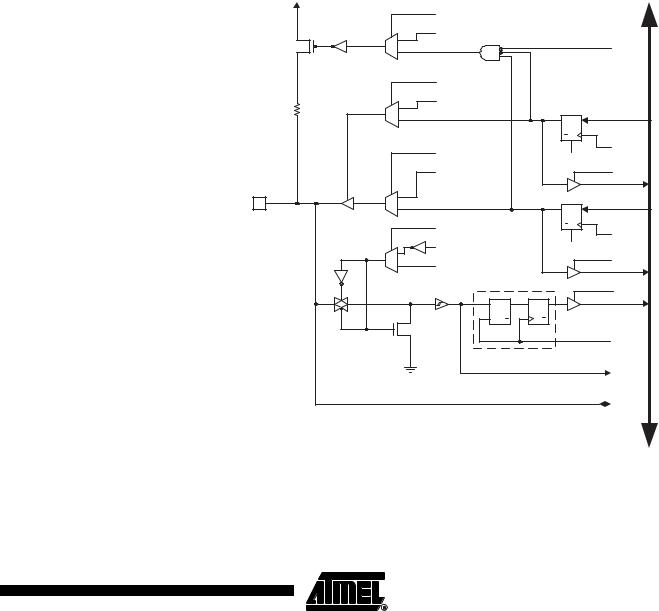
Most port pins have alternate functions in addition to being general digital I/Os. Figure 33 shows how the port pin control signals from the simplified Figure 30 can be overridden by alternate functions. The overriding signals may not be present in all port pins, but the figure serves as a generic description applicable to all port pins in the AVR microcontroller family.
Figure 33. Alternate Port Functions(1) |
|
|
|
|
|
|
|
|
PUOExn |
|
|
|
|
|
|
1 |
PUOVxn |
|
|
|
|
|
|
|
|
|
|
|
|
|
|
0 |
|
|
|
|
|
PUD |
|
|
|
|
|
|
|
|
|
|
DDOExn |
|
|
|
|
|
|
1 |
DDOVxn |
|
|
|
|
|
|
|
|
|
|
|
|
|
|
0 |
|
|
|
Q |
D |
|
|
|
|
|
|
DDxn |
|
|
|
|
|
|
|
Q CLR |
|
|
|
|
PVOExn |
|
|
|
|
WDx |
|
|
|
|
RESET |
|
|
||
|
|
|
|
|
|
||
|
PVOVxn |
|
|
|
|
RDx |
BUS |
Pxn |
|
|
|
|
|
|
|
1 |
|
|
|
|
|
|
|
0 |
|
|
|
Q |
D |
|
DATA |
|
|
|
|
PORTxn |
|
||
|
DIEOExn |
|
|
Q CLR |
|
WPx |
|
|
|
|
|
|
|
|
|
1 |
DIEOVxn |
|
|
RESET |
|
|
|
|
|
|
|
|
RRx |
|
|
0 |
SLEEP |
|
|
|
|
|
|
|
|
|
|
|
|
||
|
SYNCHRONIZER |
|
RPx |
|
|||
|
|
|
|
|
|
|
|
|
D SET |
Q |
D |
Q |
|
|
|
|
|
|
PINxn |
|
|
|
|
|
L CLR |
Q |
|
CLR Q |
|
|
|
|
|
|
|
|
|
clk I/O |
|
|
|
|
|
|
|
DIxn |
|
|
|
|
|
|
|
AIOxn |
|
PUOExn: |
Pxn PULL-UP OVERRIDE ENABLE |
PUD: |
PULLUP DISABLE |
PUOVxn: |
Pxn PULL-UP OVERRIDE VALUE |
WDx: |
WRITE DDRx |
DDOExn: |
Pxn DATA DIRECTION OVERRIDE ENABLE |
RDx: |
READ DDRx |
DDOVxn: |
Pxn DATA DIRECTION OVERRIDE VALUE |
RRx: |
READ PORTx REGISTER |
PVOExn: |
Pxn PORT VALUE OVERRIDE ENABLE |
WPx: |
WRITE PORTx |
PVOVxn: |
Pxn PORT VALUE OVERRIDE VALUE |
RPx: |
READ PORTx PIN |
DIEOExn: |
Pxn DIGITAL INPUT-ENABLE OVERRIDE ENABLE |
clk : |
I/O CLOCK |
DIEOVxn: |
Pxn DIGITAL INPUT-ENABLE OVERRIDE VALUE |
I/O |
DIGITAL INPUT PIN n ON PORTx |
DIxn: |
|||
SLEEP: |
SLEEP CONTROL |
AIOxn: |
ANALOG INPUT/OUTPUT PIN n ON PORTx |
Note: 1. WPx, WDx, RRx, RPx, and RDx are common to all pins within the same port. clkI/O,
SLEEP, and PUD are common to all ports. All other signals are unique for each pin.
63
2512G–AVR–03/05

Table 25 summarizes the function of the overriding signals. The pin and port indexes from Figure 33 are not shown in the succeeding tables. The overriding signals are generated internally in the modules having the alternate function.
Table 25. Generic Description of Overriding Signals for Alternate Functions.
Signal Name |
Full Name |
Description |
|
|
|
PUOE |
Pull-up Override |
If this signal is set, the pull-up enable is controlled by the |
|
Enable |
PUOV signal. If this signal is cleared, the pull-up is |
|
|
enabled when {DDxn, PORTxn, PUD} = 0b010. |
|
|
|
PUOV |
Pull-up Override |
If PUOE is set, the pull-up is enabled/disabled when |
|
Value |
PUOV is set/cleared, regardless of the setting of the |
|
|
DDxn, PORTxn, and PUD Register bits. |
|
|
|
DDOE |
Data Direction |
If this signal is set, the Output Driver Enable is controlled |
|
Override Enable |
by the DDOV signal. If this signal is cleared, the Output |
|
|
driver is enabled by the DDxn Register bit. |
|
|
|
DDOV |
Data Direction |
If DDOE is set, the Output Driver is enabled/disabled |
|
Override Value |
when DDOV is set/cleared, regardless of the setting of the |
|
|
DDxn Register bit. |
|
|
|
PVOE |
Port Value |
If this signal is set and the Output Driver is enabled, the |
|
Override Enable |
port value is controlled by the PVOV signal. If PVOE is |
|
|
cleared, and the Output Driver is enabled, the port Value |
|
|
is controlled by the PORTxn Register bit. |
|
|
|
PVOV |
Port Value |
If PVOE is set, the port value is set to PVOV, regardless of |
|
Override Value |
the setting of the PORTxn Register bit. |
|
|
|
DIEOE |
Digital Input |
If this bit is set, the Digital Input Enable is controlled by the |
|
Enable Override |
DIEOV signal. If this signal is cleared, the Digital Input |
|
Enable |
Enable is determined by MCU-state (Normal mode, sleep |
|
|
modes). |
|
|
|
DIEOV |
Digital Input |
If DIEOE is set, the Digital Input is enabled/disabled when |
|
Enable Override |
DIEOV is set/cleared, regardless of the MCU state |
|
Value |
(Normal mode, sleep modes). |
|
|
|
DI |
Digital Input |
This is the Digital Input to alternate functions. In the figure, |
|
|
the signal is connected to the output of the schmitt trigger |
|
|
but before the synchronizer. Unless the Digital Input is |
|
|
used as a clock source, the module with the alternate |
|
|
function will use its own synchronizer. |
|
|
|
AIO |
Analog |
This is the Analog Input/Output to/from alternate functions. |
|
Input/output |
The signal is connected directly to the pad, and can be |
|
|
used bi-directionally. |
|
|
|
The following subsections shortly describe the alternate functions for each port, and relate the overriding signals to the alternate function. Refer to the alternate function description for further details.
64 ATmega8515(L)
2512G–AVR–03/05

 ATmega8515(L)
Special Function IO Register –
SFIOR
Bit |
7 |
6 |
5 |
4 |
3 |
2 |
1 |
0 |
|
|
– |
XMBK |
XMM2 |
XMM1 |
XMM0 |
PUD |
– |
PSR10 |
SFIOR |
Read/Write |
R/W |
R/W |
R/W |
R/W |
R/W |
R/W |
R/W |
R/W |
|
Initial Value |
0 |
0 |
0 |
0 |
0 |
0 |
0 |
0 |
|
• Bit 2 – PUD: Pull-up Disable
When this bit is written to one, the pull-ups in the I/O ports are disabled even if the DDxn and PORTxn Registers are configured to enable the pull-ups ({DDxn, PORTxn} = 0b01). See “Configuring the Pin” on page 59 for more details about this feature.
Alternate Functions of Port A Port A has an alternate function as the address low byte and data lines for the External Memory Interface.
Table 26. Port A Pins Alternate Functions
Port Pin |
Alternate Function |
|
|
PA7 |
AD7 (External memory interface address and data bit 7) |
|
|
PA6 |
AD6 (External memory interface address and data bit 6) |
|
|
PA5 |
AD5 (External memory interface address and data bit 5) |
|
|
PA4 |
AD4 (External memory interface address and data bit 4) |
|
|
PA3 |
AD3 (External memory interface address and data bit 3) |
|
|
PA2 |
AD2 (External memory interface address and data bit 2) |
|
|
PA1 |
AD1 (External memory interface address and data bit 1) |
|
|
PA0 |
AD0 (External memory interface address and data bit 0) |
|
|
Table 27 and Table 28 relate the alternate functions of Port A to the overriding signals shown in Figure 33 on page 63.
Table 27. Overriding Signals for Alternate Functions in PA7..PA4
Signal |
|
|
|
|
|
|
|
|
|
|
|
|
|
|
|
|
|
|
|
|
|
|
Name |
|
PA7/AD7 |
|
|
PA6/AD6 |
|
PA5/AD5 |
|
PA4/AD4 |
|||||||||||||
|
|
|
|
|
|
|
|
|
|
|||||||||||||
PUOE |
|
SRE |
|
|
SRE |
|
SRE |
|
SRE |
|||||||||||||
|
|
|
|
|
|
|
|
|
|
|
|
|
|
|
|
|
|
|
|
|
|
|
PUOV |
|
|
|
|
| ADA(1)) • |
|
|
|
|
|
|
|
|
|
|
|
|
|
|
|
|
|
|
~(WR |
|
|
~(WR | ADA) • |
|
~(WR | ADA) • |
|
~(WR | ADA) • |
||||||||||||||
|
|
PortA7 |
|
|
PortA6 |
|
PortA5 |
|
PortA4 |
|||||||||||||
|
|
|
|
|
|
|||||||||||||||||
DDOE |
SRE |
|
SRE |
SRE |
SRE |
|||||||||||||||||
|
|
|
|
|
|
|
|
|
|
|
|
|
|
|||||||||
DDOV |
|
|
|
| ADA |
|
|
|
|
| ADA |
|
|
|
| ADA |
|
|
|
| ADA |
|||||
|
WR |
WR |
WR |
WR |
||||||||||||||||||
|
|
|
|
|
|
|
|
|
|
|||||||||||||
PVOE |
|
SRE |
|
|
SRE |
|
SRE |
|
SRE |
|||||||||||||
|
|
|
|
|
|
|
|
|
|
|||||||||||||
PVOV |
|
A7 • ADA | |
|
|
A6 • ADA | |
|
A5 • ADA | |
|
A4 • ADA | |
|||||||||||||
|
|
D7 OUTPUT • |
|
|
|
D6 OUTPUT • |
|
D5 OUTPUT • |
|
D4 OUTPUT • |
||||||||||||
|
|
WR |
|
|
|
|
||||||||||||||||
|
|
|
|
|
|
|
|
|
WR |
|
|
WR |
|
|
WR |
|
||||||
|
|
|
|
|
|
|
|
|
|
|
|
|
|
|
|
|
|
|
||||
DIEOE |
0 |
|
|
|
|
|
0 |
|
|
|
0 |
|
|
|
0 |
|
|
|
||||
|
|
|
|
|
|
|
|
|
|
|
|
|
|
|
|
|
|
|
||||
DIEOV |
0 |
|
|
|
|
|
0 |
|
|
|
0 |
|
|
|
0 |
|
|
|
||||
|
|
|
|
|
|
|
||||||||||||||||
DI |
|
D7 INPUT |
|
D6 INPUT |
D5 INPUT |
D4 INPUT |
||||||||||||||||
|
|
|
|
|
|
|
|
|
|
|||||||||||||
AIO |
|
– |
|
|
– |
|
– |
|
– |
|||||||||||||
|
|
|
|
|
|
|
|
|
|
|
|
|
|
|
|
|
|
|
|
|
|
|
Note: 1. ADA is short for ADdress Active and represents the time when address is output. See “External Memory Interface” on page 24.
65
2512G–AVR–03/05

Table 28. Overriding Signals for Alternate Functions in PA3..PA0
Signal |
|
|
|
|
|
|
|
|
|
|
|
|
|
|
|
|
|
|
|
|
Name |
|
PA3/AD3 |
PA2/AD2 |
PA1/AD1 |
PA0/AD0 |
|||||||||||||||
|
|
|
|
|
|
|
|
|||||||||||||
PUOE |
|
SRE |
|
SRE |
SRE |
|
SRE |
|||||||||||||
|
|
|
|
|
|
|
|
|
|
|
|
|
|
|
|
|
|
|
|
|
PUOV |
|
|
|
|
| ADA) • |
|
|
|
|
|
|
|
|
|
|
|
|
|
|
|
~(WR |
|
~(WR | ADA) • |
|
~(WR | ADA) • |
|
~(WR | ADA) • |
||||||||||||||
|
|
PortA3 |
|
PortA2 |
|
PortA1 |
|
PortA0 |
||||||||||||
|
|
|
|
|
||||||||||||||||
DDOE |
SRE |
SRE |
SRE |
SRE |
||||||||||||||||
|
|
|
|
|
|
|
|
|
|
|
|
|
||||||||
DDOV |
|
|
|
| ADA |
|
|
|
| ADA |
|
|
|
| ADA |
|
|
|
| ADA |
||||
|
WR |
WR |
WR |
WR |
||||||||||||||||
|
|
|
|
|
|
|
||||||||||||||
PVOE |
|
SRE |
|
SRE |
SRE |
SRE |
||||||||||||||
|
|
|
|
|
|
|
|
|
||||||||||||
PVOV |
|
A3 • ADA | |
|
A2 • ADA | |
|
A1 • ADA | |
|
A0 • ADA | |
||||||||||||
|
|
D3 OUTPUT • |
|
D2 OUTPUT • |
|
D1 OUTPUT • |
|
D0 OUTPUT • |
||||||||||||
|
|
WR |
|
|
WR |
|
|
WR |
|
|
WR |
|
||||||||
|
|
|
|
|
|
|
|
|
|
|
|
|
|
|
|
|
||||
DIEOE |
0 |
|
|
|
0 |
|
|
|
0 |
|
|
|
0 |
|
|
|
||||
|
|
|
|
|
|
|
|
|
|
|
|
|
|
|
|
|
||||
DIEOV |
0 |
|
|
|
0 |
|
|
|
0 |
|
|
|
0 |
|
|
|
||||
|
|
|
|
|
|
|
|
|
||||||||||||
DI |
|
D3 INPUT |
|
D2 INPUT |
|
D1 INPUT |
|
D0 INPUT |
||||||||||||
|
|
|
|
|
|
|
|
|
||||||||||||
AIO |
|
– |
|
– |
|
– |
|
– |
||||||||||||
|
|
|
|
|
|
|
|
|
|
|
|
|
|
|
|
|
|
|
|
|
Alternate Functions Of Port B The Port B pins with alternate functions are shown in Table 29.
Table 29. Port B Pins Alternate Functions
Port Pin |
|
Alternate Functions |
|
|
|
|
|
PB7 |
|
SCK (SPI Bus Serial Clock) |
|
|
|
|
|
PB6 |
|
MISO (SPI Bus Master Input/Slave Output) |
|
|
|
|
|
PB5 |
|
MOSI (SPI Bus Master Output/Slave Input) |
|
|
|
|
|
PB4 |
|
|
(SPI Slave Select Input) |
SS |
|||
|
|
|
|
PB3 |
|
AIN1 (Analog Comparator Negative Input) |
|
|
|
|
|
PB2 |
|
AIN0 (Analog Comparator Positive Input) |
|
|
|
|
|
PB1 |
|
T1 (Timer/Counter1 External Counter Input) |
|
|
|
|
|
PB0 |
|
T0 (Timer/Counter0 External Counter Input) |
|
|
OC0 (Timer/Counter0 Output Compare Match Output) |
||
|
|
||
|
|
|
|
The alternate pin configuration is as follows:
• SCK – Port B, Bit 7
SCK: Master Clock output, Slave Clock input pin for SPI channel. When the SPI is enabled as a Slave, this pin is configured as an input regardless of the setting of DDB7. When the SPI is enabled as a Master, the data direction of this pin is controlled by DDB7. When the pin is forced by the SPI to be an input, the pull-up can still be controlled by the PORTB7 bit.
• MISO – Port B, Bit 6
MISO: Master Data input, Slave Data output pin for SPI channel. When the SPI is enabled as a Master, this pin is configured as an input regardless of the setting of DDB6. When the SPI is enabled as a Slave, the data direction of this pin is controlled by DDB6. When the pin is forced by the SPI to be an input, the pull-up can still be controlled by the PORTB6 bit.
66 ATmega8515(L)
2512G–AVR–03/05

ATmega8515(L)
• MOSI – Port B, Bit 5
MOSI: SPI Master Data output, Slave Data input for SPI channel. When the SPI is enabled as a Slave, this pin is configured as an input regardless of the setting of DDB5. When the SPI is enabled as a Master, the data direction of this pin is controlled by DDB5. When the pin is forced by the SPI to be an input, the pull-up can still be controlled by the PORTB5 bit.
• SS – Port B, Bit 4
SS: Slave Select input. When the SPI is enabled as a Slave, this pin is configured as an input regardless of the setting of DDB4. As a Slave, the SPI is activated when this pin is driven low. When the SPI is enabled as a Master, the data direction of this pin is controlled by DDB4. When the pin is forced by the SPI to be an input, the pull-up can still be controlled by the PORTB4 bit.
• AIN1 – Port B, Bit 3
AIN1, Analog Comparator Negative input. Configure the port pin as input with the internal pull-up switched off to avoid the digital port function from interfering with the function of the Analog Comparator.
• AIN0 – Port B, Bit 2
AIN0, Analog Comparator Positive input. Configure the port pin as input with the internal pull-up switched off to avoid the digital port function from interfering with the function of the Analog Comparator.
• T1 – Port B, Bit 1
T1, Timer/Counter1 Counter Source.
• T0/OC0 – Port B, Bit 0
T0, Timer/Counter0 Counter Source.
OC0, Output Compare Match output: The PB0 pin can serve as an external output for the Timer/Counter0 Compare Match. The PB0 pin has to be configured as an output (DDB0 set (one)) to serve this function. The OC0 pin is also the output pin for the PWM mode timer function.
Table 31 relate the alternate functions of Port B to the overriding signals shown in Figure 33 on page 63. SPI MSTR INPUT and SPI SLAVE OUTPUT constitute the MISO signal, while MOSI is divided into SPI MSTR OUTPUT and SPI SLAVE INPUT.
67
2512G–AVR–03/05

Table 30. Overriding Signals for Alternate Functions in PB7..PB4
Signal |
|
|
|
|
|
|
|
|
|
|
|
|
|
|
|
|
|
|
|
|
|
|
|
|
|
Name |
PB7/SCK |
PB6/MISO |
PB5/MOSI |
PB4/SS |
|
|
|
|
|||||||||||||||||
|
|
|
|
|
|
|
|
|
|
|
|
|
|
|
|
|
|
|
|||||||
PUOE |
SPE • |
|
|
|
|
|
SPE • MSTR |
SPE • |
|
|
|
|
SPE • |
|
|
|
|
|
|
||||||
MSTR |
MSTR |
MSTR |
|
||||||||||||||||||||||
|
|
|
|
|
|
|
|
|
|
|
|
|
|
|
|||||||||||
PUOV |
PORTB7 • |
|
|
|
|
PORTB6 • |
|
|
|
PORTB5 • |
|
|
|
PORTB4 • |
|
|
|
||||||||
PUD |
PUD |
PUD |
PUD |
|
|||||||||||||||||||||
|
|
|
|
|
|
|
|
|
|
|
|
|
|||||||||||||
DDOE |
SPE • |
|
|
|
|
SPE • MSTR |
SPE • |
|
|
|
SPE • |
|
|
|
|
|
|
||||||||
MSTR |
MSTR |
MSTR |
|
||||||||||||||||||||||
|
|
|
|
|
|
|
|
|
|
|
|
|
|
|
|
|
|
|
|
|
|
|
|
|
|
DDOV |
0 |
|
|
|
|
|
0 |
|
|
|
|
0 |
|
|
|
|
0 |
|
|
|
|
|
|
|
|
|
|
|
|
|
|
|
|
|
|
|
|
|
|
|
|||||||||||
PVOE |
SPE • MSTR |
SPE • |
|
|
|
SPE • MSTR |
0 |
|
|
|
|
|
|
|
|
||||||||||
MSTR |
|
|
|
|
|
|
|
||||||||||||||||||
|
|
|
|
|
|
|
|
|
|
|
|
|
|||||||||||||
PVOV |
SCK OUTPUT |
SPI SLAVE |
SPI MSTR |
0 |
|
|
|
|
|
|
|
|
|||||||||||||
|
|
|
|
|
|
|
OUTPUT |
OUTPUT |
|
|
|
|
|
|
|
|
|
||||||||
|
|
|
|
|
|
|
|
|
|
|
|
|
|
|
|
|
|
|
|
|
|
|
|
|
|
DIEOE |
0 |
|
|
|
|
|
0 |
|
|
|
|
0 |
|
|
|
|
0 |
|
|
|
|
|
|
|
|
|
|
|
|
|
|
|
|
|
|
|
|
|
|
|
|
|
|
|
|
|
|
|
|
|
|
DIEOV |
0 |
|
|
|
|
|
0 |
|
|
|
|
0 |
|
|
|
|
0 |
|
|
|
|
|
|
|
|
|
|
|
|
|
|
|
|
||||||||||||||||||
DI |
SCK INPUT |
SPI MSTR INPUT |
SPI SLAVE INPUT |
SPI |
|
|
|
|
|
||||||||||||||||
SS |
|
||||||||||||||||||||||||
|
|
|
|
|
|
||||||||||||||||||||
AIO |
– |
– |
– |
– |
|
||||||||||||||||||||
|
|
|
|
|
|
|
|
|
|
|
|
|
|
|
|
|
|
|
|
|
|
|
|
|
|
Table 31. Overriding Signals for Alternate Functions in PB3..PB0
Signal Name |
PB3/AIN1 |
PB2/AIN0 |
PB1/T1 |
PB0/T0/OC0 |
|
|
|
|
|
PUOE |
0 |
0 |
0 |
0 |
|
|
|
|
|
PUOV |
0 |
0 |
0 |
0 |
|
|
|
|
|
DDOE |
0 |
0 |
0 |
0 |
|
|
|
|
|
DDOV |
1 |
0 |
0 |
0 |
|
|
|
|
|
PVOE |
0 |
0 |
0 |
OC0 ENABLE |
|
|
|
|
|
PVOV |
0 |
0 |
0 |
OC0 |
|
|
|
|
|
DIEOE |
0 |
0 |
0 |
0 |
|
|
|
|
|
DIEOV |
0 |
0 |
0 |
0 |
|
|
|
|
|
DI |
– |
0 |
T1 INPUT |
T0 INPUT |
|
|
|
|
|
AIO |
AIN1 INPUT |
AIN0 INPUT |
– |
– |
|
|
|
|
|
68 ATmega8515(L)
2512G–AVR–03/05