


Ordering Information
Speed (MHz) |
Power Supply |
Ordering Code |
Package(1) |
Operation Range |
|
|
ATmega8515L-8AC |
44A |
|
|
|
ATmega8515L-8PC |
40P6 |
Commercial |
|
|
ATmega8515L-8JC |
44J |
(0°C to 70°C) |
|
|
ATmega8515L-8MC(2) |
44M1 |
|
|
|
ATmega8515L-8AI |
44A |
|
8 |
2.7 - 5.5V |
ATmega8515L-8PI |
40P6 |
|
|
|
ATmega8515L-8JI |
44J |
Industrial |
|
|
ATmega8515L-8MI |
44M1 |
|
|
|
(-40°C to 85°C) |
||
|
|
ATmega8515L-8AU(2) |
44A |
|
|
|
|
||
|
|
ATmega8515L-8PU(2) |
40P6 |
|
|
|
ATmega8515L-8MU(2) |
44M1 |
|
|
|
ATmega8515-16AC |
44A |
|
|
|
ATmega8515-16PC |
40P6 |
Commercial |
|
|
ATmega8515-16JC |
44J |
(0°C to 70°C) |
|
|
ATmega8515-16MC |
44M1 |
|
|
|
|
|
|
|
|
ATmega8515-16AI |
44A |
|
16 |
4.5 - 5.5V |
ATmega8515-16PI |
40P6 |
|
|
|
ATmega8515-16JI |
44J |
Industrial |
|
|
ATmega8515-16MI |
44M1 |
|
|
|
(-40°C to 85°C) |
||
|
|
ATmega8515-16AU(2) |
44A |
|
|
|
|
||
|
|
ATmega8515-16PU(2) |
40P6 |
|
|
|
ATmega8515-16MU(2) |
44MI |
|
Note: 1. |
This device can also be supplied in wafer form. Please contact your local Atmel sales office for detailed ordering information |
|
and minimum quantities.. |
2. |
Pb-free packaging alternative, complies to the European Directive for Restriction of Hazardous Substances (RoHS direc- |
|
tive).Also Halide free and fully Green. |
|
Package Type |
|
|
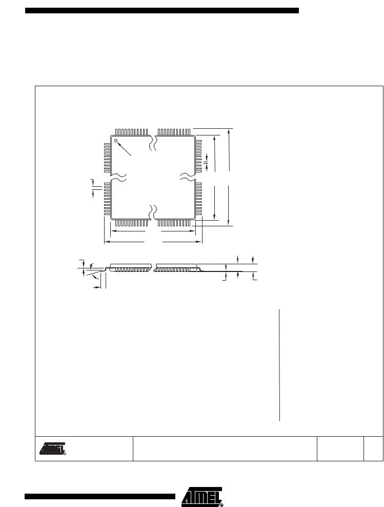
44A |
44-lead, Thin (1.0 mm) Plastic Gull Wing Quad Flat Package (TQFP) |
|
|
40P6 |
40-lead, 0.600” Wide, Plastic Dual Inline Package (PDIP) |
|
|
44J |
44-lead, Plastic J-Leaded Chip Carrier (PLCC) |
|
|
44M1 |
44-pad, 7 x 7 x 1.0 mm body, lead pitch 0.50 mm, Quad Flat No-Lead/Micro Lead Frame Package (QFN/MLF) |
|
|
242 ATmega8515(L)
2512G–AVR–03/05

 L
L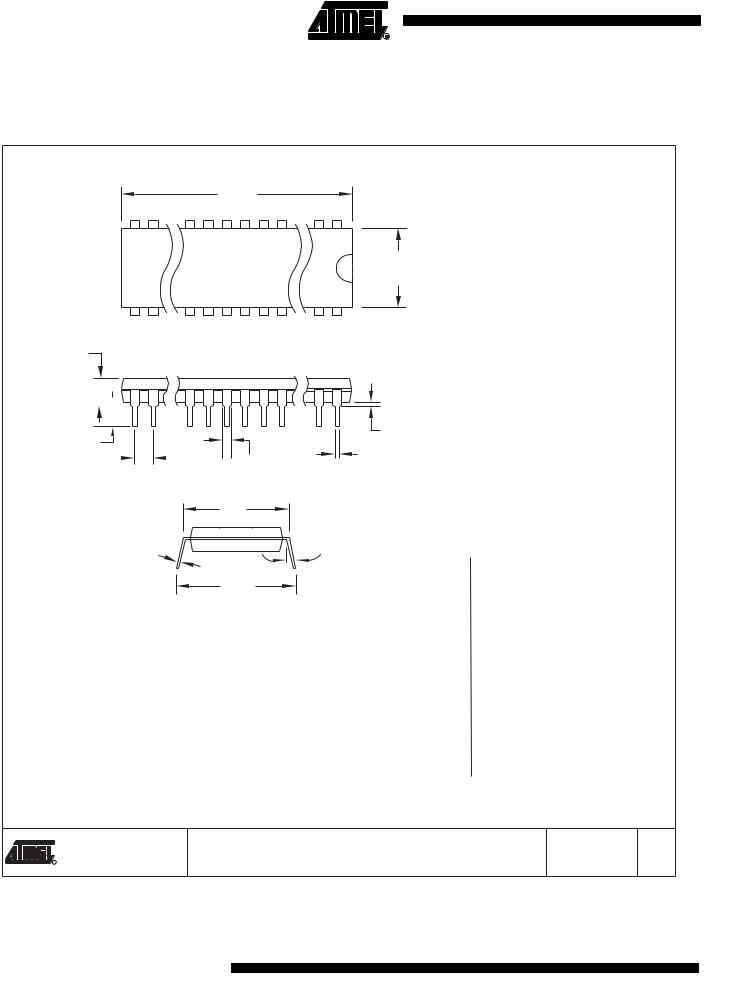


 B1 e
B1 e

 Marked Pin# 1 ID