- •Features
- •Pin Configurations
- •Overview
- •Block Diagram
- •Disclaimer
- •Pin Descriptions
- •Port A (PA7..PA0)
- •Port B (PB7..PB0)
- •Port C (PC7..PC0)
- •Port D (PD7..PD0)
- •Port E(PE2..PE0)
- •RESET
- •XTAL1
- •XTAL2
- •AVR CPU Core
- •Introduction
- •Architectural Overview
- •Status Register
- •Stack Pointer
- •Interrupt Response Time
- •In-System Reprogrammable Flash Program memory
- •SRAM Data Memory
- •Data Memory Access Times
- •EEPROM Data Memory
- •EEPROM Read/Write Access
- •I/O Memory
- •Overview
- •Address Latch Requirements
- •Pull-up and Bus Keeper
- •Timing
- •Using all Locations of External Memory Smaller than 64 KB
- •Using all 64KB Locations of External Memory
- •Clock Systems and their Distribution
- •Clock Sources
- •Default Clock Source
- •Crystal Oscillator
- •External RC Oscillator
- •External Clock
- •Idle Mode
- •Power-down Mode
- •Standby Mode
- •Analog Comparator
- •Brown-out Detector
- •Internal Voltage Reference
- •Watchdog Timer
- •Port Pins
- •Resetting the AVR
- •Reset Sources
- •Power-on Reset
- •External Reset
- •Brown-out Detection
- •Watchdog Reset
- •Watchdog Timer
- •Timed Sequences for Changing the Configuration of the Watchdog Timer
- •Safety Level 0
- •Safety Level 1
- •Safety Level 2
- •Interrupts
- •Moving Interrupts between Application and Boot Space
- •I/O Ports
- •Introduction
- •Configuring the Pin
- •Reading the Pin Value
- •Unconnected pins
- •Alternate Port Functions
- •Alternate Functions of Port A
- •Alternate Functions Of Port B
- •Alternate Functions of Port C
- •Alternate Functions of Port D
- •Alternate Functions of Port E
- •Register Description for I/O Ports
- •External Interrupts
- •8-bit Timer/Counter0 with PWM
- •Overview
- •Registers
- •Definitions
- •Counter Unit
- •Output Compare Unit
- •Force Output Compare
- •Modes of Operation
- •Normal Mode
- •Fast PWM Mode
- •Phase Correct PWM Mode
- •Internal Clock Source
- •Prescaler Reset
- •External Clock Source
- •16-bit Timer/Counter1
- •Overview
- •Registers
- •Definitions
- •Compatibility
- •Counter Unit
- •Input Capture Unit
- •Input Capture Trigger Source
- •Noise Canceler
- •Using the Input Capture Unit
- •Output Compare Units
- •Force Output Compare
- •Modes of Operation
- •Normal Mode
- •Fast PWM Mode
- •Phase Correct PWM Mode
- •Slave Mode
- •Master Mode
- •Data Modes
- •USART
- •Single USART
- •Clock Generation
- •External Clock
- •Synchronous Clock Operation
- •Frame Formats
- •Parity Bit Calculation
- •USART Initialization
- •Sending Frames with 5 to 8 Data Bits
- •Sending Frames with 9 Data Bits
- •Parity Generator
- •Disabling the Transmitter
- •Receiving Frames with 5 to 8 Data Bits
- •Receiving Frames with 9 Data Bits
- •Receiver Error Flags
- •Parity Checker
- •Disabling the Receiver
- •Flushing the Receive Buffer
- •Asynchronous Data Recovery
- •Using MPCM
- •Write Access
- •Read Access
- •Analog Comparator
- •Features
- •Application Section
- •Boot Loader Lock bits
- •Performing a Page Write
- •Using the SPM Interrupt
- •Setting the Boot Loader Lock bits by SPM
- •Reading the Fuse and Lock bits from Software
- •Preventing Flash Corruption
- •Simple Assembly Code Example for a Boot Loader
- •Program and Data Memory Lock bits
- •Fuse bits
- •Latching of Fuses
- •Signature Bytes
- •Calibration Byte
- •Calibration Byte
- •Signal Names
- •Parallel Programming
- •Enter Programming Mode
- •Chip Erase
- •Programming the Flash
- •Programming the EEPROM
- •Reading the Flash
- •Reading the EEPROM
- •Programming the Lock bits
- •Reading the Signature Bytes
- •Reading the Calibration Byte
- •Serial Downloading
- •Data Polling Flash
- •Data Polling EEPROM
- •Electrical Characteristics
- •Absolute Maximum Ratings*
- •External Clock Drive Waveforms
- •External Clock Drive
- •External Data Memory Timing
- •Active Supply Current
- •Idle Supply Current
- •Standby Supply Current
- •Pin Pull-up
- •Pin Driver Strength
- •Internal Oscillator Speed
- •Register Summary
- •Instruction Set Summary
- •Ordering Information
- •Packaging Information
- •Errata
- •ATmega8515(L) Rev. B
- •Changes from Rev. 2512F-12/03 to Rev. 2512G-03/05
- •Changes from Rev. 2512F-12/03 to Rev. 2512E-09/03
- •Changes from Rev. 2512D-02/03 to Rev. 2512E-09/03
- •Changes from Rev. 2512C-10/02 to Rev. 2512D-02/03
- •Changes from Rev. 2512B-09/02 to Rev. 2512C-10/02
- •Changes from Rev. 2512A-04/02 to Rev. 2512B-09/02
- •Table of Contents
|
|
|
|
|
|
|
|
|
|
|
|
|
|
|
ATmega8515(L) |
||
|
|
|
|
|
|
|
|
|
|
|
|
|
|
|
|||
|
External Reset |
|
|
|
|
|
|
|
|
|
|
|
|
|
|||
|
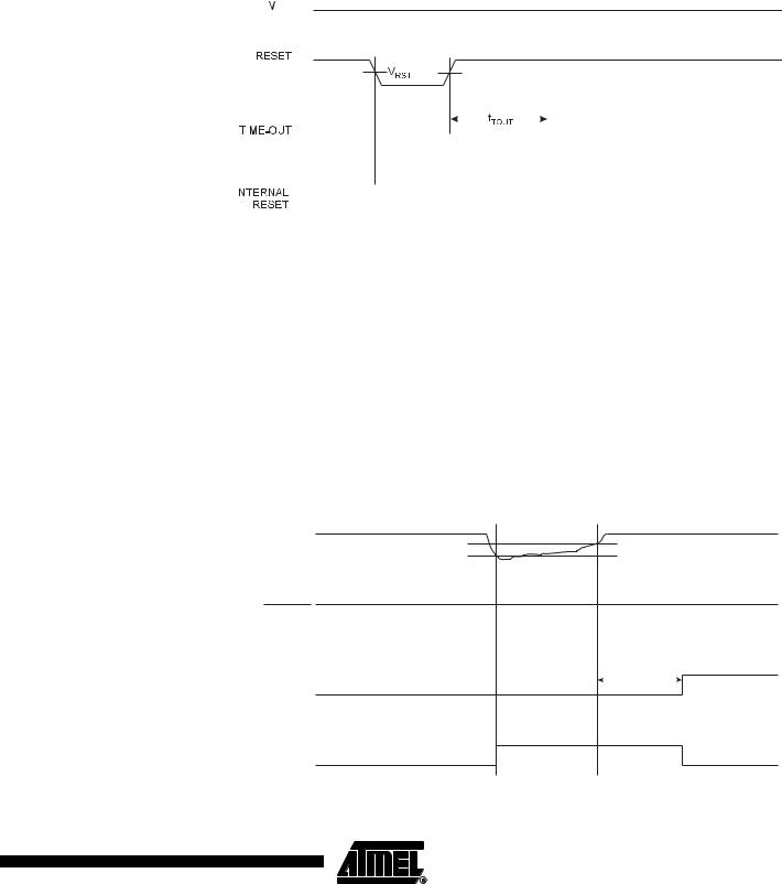
An External Reset is generated by a low level on the |
|
pin. Reset pulses longer |
||||||||||||||
|
|
||||||||||||||||
|
RESET |
||||||||||||||||
|
|
than the minimum pulse width (see Table 18) will generate a reset, even if the clock is |
|||||||||||||||
|
|
not running. Shorter pulses are not guaranteed to generate a reset. When the applied |
|||||||||||||||
|
|
signal reaches the Reset Threshold Voltage – VRST – on its positive edge, the delay |
|||||||||||||||
|
|
counter starts the MCU after the Time-out period tTOUT has expired. |
|||||||||||||||
|
|
Figure 25. External Reset During Operation |
|||||||||||||||
|
|
|
|
|
CC |
||||||||||||
|
|
|
|
|
|
|
|
|
|
|
|
|
|
|
|
|
|
|
|
|
|
|
|
|
|
|
|
|
|
|
|
|
|
|
|
|
|
|
|
|
|
|
|
|
|
|
|
|
|
|
|
|
|
|
|
|
|
|
|
|
|
|
|
|
|
|
|
|
|
|
|
|
|
|
|
|
|
|
|
|
|
|
|
|
|
|
|
|
|
|
|
|
|
|
|
|
|
|
|
|
|
|
|
|
|
|
|
|
|
|
|
|
|
|
|
|
|
|
|
|
|
|
|
|
|
|
|
|
|
|
|
|
|
|
|
|
|
|
|
|
|
|
|
Brown-out Detection |
ATmega8515 has an On-chip Brown-out Detection (BOD) circuit for monitoring the VCC |
|
level during operation by comparing it to a fixed trigger level. The trigger level for the |
|
BOD can be selected by the fuse BODLEVEL to be 2.7V (BODLEVEL unprogrammed), |
|
or 4.0V (BODLEVEL programmed). The trigger level has a hysteresis to ensure spike |
|
free Brown-out Detection. The hysteresis on the detection level should be interpreted as |
|
VBOT+ = VBOT + VHYST/2 and VBOT- = VBOT - VHYST/2. |
|
The BOD circuit can be enabled/disabled by the fuse BODEN. When the BOD is |
|
enabled (BODEN programmed), and VCC decreases to a value below the trigger level |
|
(VBOT- in Figure 26), the Brown-out Reset is immediately activated. When VCC increases |
|
above the trigger level (VBOT+ in Figure 26), the delay counter starts the MCU after the |
|
time-out period tTOUT has expired. |
|
The BOD circuit will only detect a drop in VCC if the voltage stays below the trigger level |
|
for longer than tBOD given in Table 18. |
|
Figure 26. Brown-out Reset During Operation |
VCC |
VBOT+ |
|
VBOT- |
RESET |
|
TIME-OUT |
tTOUT |
INTERNAL |
|
RESET |
|
47
2512G–AVR–03/05
Watchdog Reset |
|
|
|
|
|
|
|
|
|
|
|
|
|
|
|
|
|
|
|
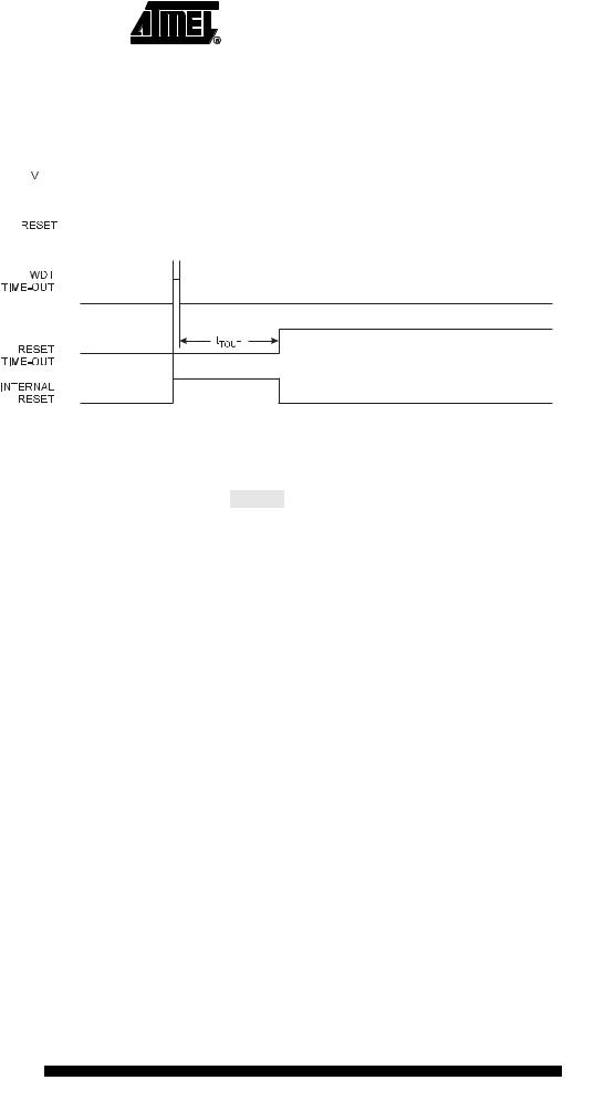
When the Watchdog times out, it will generate a short reset pulse of one CK cycle dura- |
|||||||||
|
tion. On the falling edge of this pulse, the delay timer starts counting the Time-out period |
||||||||
|
tTOUT. Refer to page 52 for details on operation of the Watchdog Timer. |
||||||||
|
Figure 27. Watchdog Reset During Operation |
||||||||
|
|
CC |
|
|
|||||
|
|
||||||||
|
|
|
|
|
|
|
|
|
|
|
|
|
|
|
|
|
|
|
|
CK
MCU Control and Status |
The MCU Control and Status Register provides information on which reset source |
|||||||||
Register – MCUCSR |
caused an MCU Reset. |
|
|
|
|
|
|
|
||
|
Bit |
7 |
6 |
5 |
4 |
3 |
2 |
1 |
0 |
|
|
|
|
|
|
|
|
|
|
|
|
|
|
– |
– |
SM2 |
– |
WDRF |
BORF |
EXTRF |
PORF |
MCUCSR |
|
Read/Write |
R/W |
R/W |
R |
R/W |
R/W |
R/W |
R/W |
R/W |
|
|
Initial Value |
0 |
0 |
0 |
|
See Bit Description |
|
|
• Bit 3 – WDRF: Watchdog Reset Flag
This bit is set if a Watchdog Reset occurs. The bit is reset by a Power-on Reset, or by writing a logic zero to the flag.
• Bit 2 – BORF: Brown-out Reset Flag
This bit is set if a Brown-out Reset occurs. The bit is reset by a Power-on Reset, or by writing a logic zero to the flag.
• Bit 1 – EXTRF: External Reset Flag
This bit is set if an External Reset occurs. The bit is reset by a Power-on Reset, or by writing a logic zero to the flag.
• Bit 0 – PORF: Power-on Reset Flag
This bit is set if a Power-on Reset occurs. The bit is reset only by writing a logic zero to the flag.
To make use of the Reset Flags to identify a reset condition, the user should read and then reset the MCUCSR as early as possible in the program. If the register is cleared before another reset occurs, the source of the reset can be found by examining the Reset Flags.
48 ATmega8515(L)
2512G–AVR–03/05