- •Features
- •Pin Configurations
- •Overview
- •Block Diagram
- •Disclaimer
- •Pin Descriptions
- •Port A (PA7..PA0)
- •Port B (PB7..PB0)
- •Port C (PC7..PC0)
- •Port D (PD7..PD0)
- •Port E(PE2..PE0)
- •RESET
- •XTAL1
- •XTAL2
- •AVR CPU Core
- •Introduction
- •Architectural Overview
- •Status Register
- •Stack Pointer
- •Interrupt Response Time
- •In-System Reprogrammable Flash Program memory
- •SRAM Data Memory
- •Data Memory Access Times
- •EEPROM Data Memory
- •EEPROM Read/Write Access
- •I/O Memory
- •Overview
- •Address Latch Requirements
- •Pull-up and Bus Keeper
- •Timing
- •Using all Locations of External Memory Smaller than 64 KB
- •Using all 64KB Locations of External Memory
- •Clock Systems and their Distribution
- •Clock Sources
- •Default Clock Source
- •Crystal Oscillator
- •External RC Oscillator
- •External Clock
- •Idle Mode
- •Power-down Mode
- •Standby Mode
- •Analog Comparator
- •Brown-out Detector
- •Internal Voltage Reference
- •Watchdog Timer
- •Port Pins
- •Resetting the AVR
- •Reset Sources
- •Power-on Reset
- •External Reset
- •Brown-out Detection
- •Watchdog Reset
- •Watchdog Timer
- •Timed Sequences for Changing the Configuration of the Watchdog Timer
- •Safety Level 0
- •Safety Level 1
- •Safety Level 2
- •Interrupts
- •Moving Interrupts between Application and Boot Space
- •I/O Ports
- •Introduction
- •Configuring the Pin
- •Reading the Pin Value
- •Unconnected pins
- •Alternate Port Functions
- •Alternate Functions of Port A
- •Alternate Functions Of Port B
- •Alternate Functions of Port C
- •Alternate Functions of Port D
- •Alternate Functions of Port E
- •Register Description for I/O Ports
- •External Interrupts
- •8-bit Timer/Counter0 with PWM
- •Overview
- •Registers
- •Definitions
- •Counter Unit
- •Output Compare Unit
- •Force Output Compare
- •Modes of Operation
- •Normal Mode
- •Fast PWM Mode
- •Phase Correct PWM Mode
- •Internal Clock Source
- •Prescaler Reset
- •External Clock Source
- •16-bit Timer/Counter1
- •Overview
- •Registers
- •Definitions
- •Compatibility
- •Counter Unit
- •Input Capture Unit
- •Input Capture Trigger Source
- •Noise Canceler
- •Using the Input Capture Unit
- •Output Compare Units
- •Force Output Compare
- •Modes of Operation
- •Normal Mode
- •Fast PWM Mode
- •Phase Correct PWM Mode
- •Slave Mode
- •Master Mode
- •Data Modes
- •USART
- •Single USART
- •Clock Generation
- •External Clock
- •Synchronous Clock Operation
- •Frame Formats
- •Parity Bit Calculation
- •USART Initialization
- •Sending Frames with 5 to 8 Data Bits
- •Sending Frames with 9 Data Bits
- •Parity Generator
- •Disabling the Transmitter
- •Receiving Frames with 5 to 8 Data Bits
- •Receiving Frames with 9 Data Bits
- •Receiver Error Flags
- •Parity Checker
- •Disabling the Receiver
- •Flushing the Receive Buffer
- •Asynchronous Data Recovery
- •Using MPCM
- •Write Access
- •Read Access
- •Analog Comparator
- •Features
- •Application Section
- •Boot Loader Lock bits
- •Performing a Page Write
- •Using the SPM Interrupt
- •Setting the Boot Loader Lock bits by SPM
- •Reading the Fuse and Lock bits from Software
- •Preventing Flash Corruption
- •Simple Assembly Code Example for a Boot Loader
- •Program and Data Memory Lock bits
- •Fuse bits
- •Latching of Fuses
- •Signature Bytes
- •Calibration Byte
- •Calibration Byte
- •Signal Names
- •Parallel Programming
- •Enter Programming Mode
- •Chip Erase
- •Programming the Flash
- •Programming the EEPROM
- •Reading the Flash
- •Reading the EEPROM
- •Programming the Lock bits
- •Reading the Signature Bytes
- •Reading the Calibration Byte
- •Serial Downloading
- •Data Polling Flash
- •Data Polling EEPROM
- •Electrical Characteristics
- •Absolute Maximum Ratings*
- •External Clock Drive Waveforms
- •External Clock Drive
- •External Data Memory Timing
- •Active Supply Current
- •Idle Supply Current
- •Standby Supply Current
- •Pin Pull-up
- •Pin Driver Strength
- •Internal Oscillator Speed
- •Register Summary
- •Instruction Set Summary
- •Ordering Information
- •Packaging Information
- •Errata
- •ATmega8515(L) Rev. B
- •Changes from Rev. 2512F-12/03 to Rev. 2512G-03/05
- •Changes from Rev. 2512F-12/03 to Rev. 2512E-09/03
- •Changes from Rev. 2512D-02/03 to Rev. 2512E-09/03
- •Changes from Rev. 2512C-10/02 to Rev. 2512D-02/03
- •Changes from Rev. 2512B-09/02 to Rev. 2512C-10/02
- •Changes from Rev. 2512A-04/02 to Rev. 2512B-09/02
- •Table of Contents
Serial Downloading
Serial Programming Pin
Mapping
2512G–AVR–03/05
ATmega8515(L)
Both the Flash and EEPROM memory arrays can be programmed using the serial SPI bus while RESET is pulled to GND. The serial interface consists of pins SCK, MOSI (input) and MISO (output). After RESET is set low, the Programming Enable instruction needs to be executed first before program/erase operations can be executed.
Note: In Table 92, the pin mapping for SPI programming is listed. Not all parts use the SPI pins dedicated for the internal SPI interface.
Table 92. Pin Mapping Serial Programming
Symbol |
Pins |
I/O |
Description |
|
|
|
|
MOSI |
PB5 |
I |
Serial data in |
|
|
|
|
MISO |
PB6 |
O |
Serial data out |
|
|
|
|
SCK |
PB7 |
I |
Serial clock |
|
|
|
|
Both the Flash and EEPROM memory arrays can be programmed using the serial SPI bus while RESET is pulled to GND. The serial interface consists of pins SCK, MOSI (input) and MISO (output). After RESET is set low, the Programming Enable instruction needs to be executed first before program/erase operations can be executed. NOTE, in Table 92 on page 191, the pin mapping for SPI programming is listed. Not all parts use the SPI pins dedicated for the internal SPI interface.
Figure 84. Serial Programming and Verify(1)
VCC
MOSI
MISO
SCK
XTAL1
RESET
GND
Note: 1. If the device is clocked by the internal Oscillator, it is no need to connect a clock source to the XTAL1 pin.
When programming the EEPROM, an auto-erase cycle is built into the self-timed programming operation (in the Serial mode ONLY) and there is no need to first execute the Chip Erase instruction. The Chip Erase operation turns the content of every memory location in both the Program and EEPROM arrays into $FF.
Depending on CKSEL Fuses, a valid clock must be present. The minimum low and high periods for the serial clock (SCK) input are defined as follows:
Low: > 2 CPU clock cycles for fck < 12 MHz, 3 CPU clock cycles for fck ≥ 12 MHz High: > 2 CPU clock cycles for fck < 12 MHz, 3 CPU clock cycles for fck ≥ 12 MHz
191
Serial Programming
Algorithm
Data Polling Flash
When writing serial data to the ATmega8515, data is clocked on the rising edge of SCK.
When reading data from the ATmega8515, data is clocked on the falling edge of SCK. See Figure 85 for timing details.
To program and verify the ATmega8515 in the Serial Programming mode, the following sequence is recommended (See four byte instruction formats in Table 94.):
1.Power-up sequence:
Apply power between VCC and GND while RESET and SCK are set to “0”. In some systems, the programmer can not guarantee that SCK is held low during Power-up. In this case, RESET must be given a positive pulse of at least two CPU clock cycles duration after SCK has been set to “0”.
2.Wait for at least 20 ms and enable serial programming by sending the Programming Enable serial instruction to pin MOSI.
3.The Serial Programming instructions will not work if the communication is out of synchronization. When in synchronization, the second byte ($53), will echo back when issuing the third byte of the Programming Enable instruction. Whether the echo is correct or not, all four bytes of the instruction must be transmitted. If the $53 did not echo back, give RESET a positive pulse and issue a new Programming Enable command.
4.The Flash is programmed one page at a time. The page size is found in Table 89 on page 181. The memory page is loaded one byte at a time by supplying the 5 LSB of the address and data together with the Load Program memory Page instruction. To ensure correct loading of the page, the data low byte must be loaded before data high byte is applied for a given address. The Program memory Page is stored by loading the Write Program memory Page instruction with the 7 MSB of the address. If polling is not used, the user must wait at least
tWD_FLASH before issuing the next page, see Table 93. Accessing the serial programming interface before the Flash write operation completes can result in incorrect programming.
5.The EEPROM array is programmed one byte at a time by supplying the address and data together with the appropriate Write instruction. An EEPROM memory location is first automatically erased before new data is written. If polling is not
used, the user must wait at least tWD_EEPROM before issuing the next byte, see Table 93. In a chip erased device, no $FFs in the data file(s) need to be programmed.
6.Any memory location can be verified by using the Read instruction which returns the content at the selected address at serial output MISO.
7.At the end of the programming session, RESET can be set high to commence normal operation.
8.Power-off sequence (if needed): Set RESET to “1”.
Turn VCC power off.
When a page is being programmed into the Flash, reading an address location within the page being programmed will give the value $FF. At the time the device is ready for a new page, the programmed value will read correctly. This is used to determine when the next page can be written. Note that the entire page is written simultaneously and any address within the page can be used for polling. Data polling of the Flash will not work for the value $FF, so when programming this value, the user will have to wait for at least
tWD_FLASH before programming the next page. As a chip erased device contains $FF in all locations, programming of addresses that are meant to contain $FF, can be skipped.
See Table 93 for tWD_FLASH value.
192 ATmega8515(L)
2512G–AVR–03/05
|
|
|
|
ATmega8515(L) |
|
|
|
|
|
|
Data Polling EEPROM |
|
|
|
|
When a new byte has been written and is being programmed into EEPROM, reading the |
|||
|
||||
|
|
address location being programmed will give the value $FF. At the time the device is |
||
|
|
ready for a new byte, the programmed value will read correctly. This is used to deter- |
||
|
|
mine when the next byte can be written. This will not work for the value $FF, but the user |
||
|
|
should have the following in mind: As a chip erased device contains $FF in all locations, |
||
|
|
programming of addresses that are meant to contain $FF, can be skipped. This does |
||
|
|
not apply if the EEPROM is reprogrammed without chip-erasing the device. In this case, |
||
|
|
data polling cannot be used for the value $FF, and the user will have to wait at least |
||
|
|
tWD_EEPROM before programming the next byte. See Table 93 for tWD_EEPROM value. |
||
|
|
Table 93. Minimum Wait Delay Before Writing the Next Flash or EEPROM Location |
||
|
|
|
|
|
|
|
Symbol |
Minimum Wait Delay |
|
|
|
|
|
|
|
|
tWD_FUSE |
|
4.5 ms |
|
|
tWD_FLASH |
|
4.5 ms |
|
|
tWD_EEPROM |
|
9.0 ms |
|
|
tWD_ERASE |
|
9.0 ms |
Figure 85. Serial Programming Waveforms
SERIAL DATA INPUT |
MSB |
LSB |
(MOSI) |
|
|
SERIAL DATA OUTPUT |
MSB |
LSB |
(MISO) |
|
|
SERIAL CLOCK INPUT |
|
|
(SCK) |
|
|
SAMPLE |
|
|
193
2512G–AVR–03/05
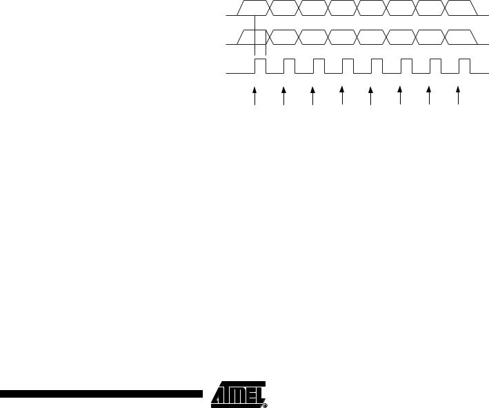
Table 94. Serial Programming Instruction Set
|
|
Instruction Format |
|
|
|
Instruction |
|
|
|
|
Operation |
Byte 1 |
Byte 2 |
Byte 3 |
Byte4 |
||
|
|
|
|
|
|
Programming Enable |
1010 1100 |
0101 0011 |
xxxx xxxx |
xxxx xxxx |
Enable Serial Programming after |
|
|
|
|
|
RESET goes low. |
Chip Erase |
1010 1100 |
100x xxxx |
xxxx xxxx |
xxxx xxxx |
Chip Erase EEPROM and Flash. |
|
0010 H000 |
0000 aaaa |
bbbb bbbb |
oooo oooo |
Read H (high or low) data o from |
Read Program memory |
|
|
|
|
Program memory at word address |
|
|
|
|
|
a:b. |
|
0100 H000 |
0000 xxxx |
xxxb bbbb |
iiii iiii |
Write H (high or low) data i to |
Load Program memory |
|
|
|
|
Program memory page at word |
|
|
|
|
address b. Data low byte must be |
|
Page |
|
|
|
|
|
|
|
|
|
loaded before Data high byte is |
|
|
|
|
|
|
|
|
|
|
|
|
applied within the same address. |
|
|
|
|
|
|
Write Program memory |
0100 1100 |
0000 aaaa |
bbbx xxxx |
xxxx xxxx |
Write Program memory Page at |
Page |
|
|
|
|
address a:b. |
Read EEPROM Memory |
1010 0000 |
00xx xxxa |
bbbb bbbb |
oooo oooo |
Read data o from EEPROM |
|
|
|
|
|
memory at address a:b. |
Write EEPROM Memory |
1100 0000 |
00xx xxxa |
bbbb bbbb |
iiii iiii |
Write data i to EEPROM memory at |
|
|
|
|
|
address a:b. |
|
0101 1000 |
0000 0000 |
xxxx xxxx |
xxoo oooo |
Read Lock bits. “0” = programmed, |
Read Lock bits |
|
|
|
|
“1” = unprogrammed. See Table |
|
|
|
|
|
81 on page 177 for details. |
|
|
|
|
|
|
|
1010 1100 |
111x xxxx |
xxxx xxxx |
11ii iiii |
Write Lock bits. Set bits = “0” to |
Write Lock bits |
|
|
|
|
program Lock bits. See Table 81 |
|
|
|
|
|
on page 177 for details. |
|
|
|
|
|
|
Read Signature Byte |
0011 0000 |
00xx xxxx |
xxxx xxbb |
oooo oooo |
Read Signature Byte o at address |
|
|
|
|
|
b. |
|
1010 1100 |
1010 0000 |
xxxx xxxx |
iiii iiii |
Set bits = “0” to program, “1” to |
Write Fuse bits |
|
|
|
|
unprogram. See Table 84 on |
|
|
|
|
|
page 179 for details. |
|
|
|
|
|
|
|
1010 1100 |
1010 1000 |
xxxx xxxx |
iiii iiii |
Set bits = “0” to program, “1” to |
Write Fuse High Bits |
|
|
|
|
unprogram. See Table 83 on |
|
|
|
|
|
page 178 for details. |
|
|
|
|
|
|
|
0101 0000 |
0000 0000 |
xxxx xxxx |
oooo oooo |
Read Fuse bits. “0” = programmed, |
Read Fuse bits |
|
|
|
|
“1” = unprogrammed. See Table |
|
|
|
|
|
84 on page 179 for details. |
|
|
|
|
|
|
|
0101 1000 |
0000 1000 |
xxxx xxxx |
oooo oooo |
Read Fuse high bits. “0” = pro- |
Read Fuse High Bits |
|
|
|
|
grammed, “1” = unprogrammed. |
|
|
|
|
See Table 83 on page 178 for |
|
|
|
|
|
|
|
|
|
|
|
|
details. |
|
|
|
|
|
|
Read Calibration Byte |
0011 1000 |
00xx xxxx |
0000 0000 |
oooo oooo |
Read Calibration Byte |
Note: a = address high bits b = address low bits
H = 0 - Low byte, 1 - High Byte o = data out
i = data in
x = don’t care
194 ATmega8515(L)
2512G–AVR–03/05