


Phase Correct PWM Mode The phase correct Pulse Width Modulation or phase correct PWM mode (WGM13:0 = 1, 2, 3, 10, or 11) provides a high resolution phase correct PWM waveform generation option. The phase correct PWM mode is, like the phase and frequency correct PWM mode, based on a dual-slope operation. The counter counts repeatedly from BOTTOM (0x0000) to TOP and then from TOP to BOTTOM. In non-inverting compare output mode, the Output Compare (OC1x) is cleared on the Compare Match between TCNT1 and OCR1x while upcounting, and set on the Compare Match while downcounting. In inverting Output Compare mode, the operation is inverted. The dual-slope operation has lower maximum operation frequency than single slope operation. However, due to the symmetric feature of the dual-slope PWM modes, these modes are preferred for motor control applications.
The PWM resolution for the phase correct PWM mode can be fixed to 8-, 9-, or 10-bit, or defined by either ICR1 or OCR1A. The minimum resolution allowed is 2-bit (ICR1 or OCR1A set to 0x0003), and the maximum resolution is 16-bit (ICR1 or OCR1A set to MAX). The PWM resolution in bits can be calculated by using the following equation:
RPCPWM = |
log(TOP + 1) |
-------------------------------log(2) --- |
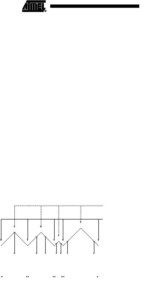
In phase correct PWM mode the counter is incremented until the counter value matches either one of the fixed values 0x00FF, 0x01FF, or 0x03FF (WGM13:0 = 1, 2, or 3), the value in ICR1 (WGM13:0 = 10), or the value in OCR1A (WGM13:0 = 11). The counter has then reached the TOP and changes the count direction. The TCNT1 value will be equal to TOP for one timer clock cycle. The timing diagram for the phase correct PWM mode is shown on Figure 54. The figure shows phase correct PWM mode when OCR1A or ICR1 is used to define TOP. The TCNT1 value is in the timing diagram shown as a histogram for illustrating the dual-slope operation. The diagram includes non-inverted and inverted PWM outputs. The small horizontal line marks on the TCNT1 slopes represent Compare Matches between OCR1x and TCNT1. The OC1x Interrupt Flag will be set when a Compare Match occurs.
Figure 54. Phase Correct PWM Mode, Timing Diagram
OCRnx/TOP Update and OCnA Interrupt Flag Set or ICFn Interrupt Flag Set (Interrupt on TOP)
TOVn Interrupt Flag Set (Interrupt on Bottom)
TCNTn
OCnx |
|
|
|
|
|
|
|
|
|
|
|
|
|
|
|
|
|
|
|
|
|
|
|
|
|
(COMnx1:0 = 2) |
|||
|
|
|
|
|
|
|
|
|
|
|
|
|
|
|
|
|
|
|
|
|
|
|
|
|
|
|
|
|
|
OCnx |
|
|
|
|
|
|
|
|
|
|
|
|
|
|
|
|
|
|
|
|
|
|
|
|
|
(COMnx1:0 = 3) |
|||
Period |
|
|
|
|
|
|
|
|
|
|
|
|
|
|
|
|
|
|
|
|
|
|
|
||||||
|
|
|
|
|
|
|
|
|
|
|
|
|
|
|
|
|
|
|
|
|
|
|
|
||||||
|
|
|
1 |
|
|
|
|
2 |
|
|
|
|
3 |
|
|
|
|
|
4 |
|
|
|
|
||||||
|
|
|
|
|
|
|
|
|
|
|
|
|
|||||||||||||||||
|
|
|
|
|
|
|
|
|
|
|
|
|
|
|
|
|
|
|
|
|
|
|
|
|
|
|
|
|
|
112 ATmega8515(L)
2512G–AVR–03/05

 ATmega8515(L)
The Timer/Counter Overflow Flag (TOV1) is set each time the counter reaches BOTTOM. When either OCR1A or ICR1 is used for defining the TOP value, the OC1A or ICF1 Flag is set accordingly at the same timer clock cycle as the OCR1x Registers are updated with the double buffer value (at TOP). The Interrupt Flags can be used to generate an interrupt each time the counter reaches the TOP or BOTTOM value.
When changing the TOP value the program must ensure that the new TOP value is higher or equal to the value of all of the compare registers. If the TOP value is lower than any of the compare registers, a Compare Match will never occur between the TCNT1 and the OCR1x. Note that when using fixed TOP values, the unused bits are masked to zero when any of the OCR1x Registers are written. As the third period shown in Figure 54 illustrates, changing the TOP actively while the Timer/Counter is running in the phase correct mode can result in an unsymmetrical output. The reason for this can be found in the time of update of the OCR1x Register. Since the OCR1x update occurs at TOP, the PWM period starts and ends at TOP. This implies that the length of the falling slope is determined by the previous TOP value, while the length of the rising slope is determined by the new TOP value. When these two values differ the two slopes of the period will differ in length. The difference in length gives the unsymmetrical result on the output.
It is recommended to use the phase and frequency correct mode instead of the phase correct mode when changing the TOP value while the Timer/Counter is running. When using a static TOP value there are practically no differences between the two modes of operation.
In phase correct PWM mode, the compare units allow generation of PWM waveforms on the OC1x pins. Setting the COM1x1:0 bits to 2 will produce a non-inverted PWM and an inverted PWM output can be generated by setting the COM1x1:0 to 3 (See Table 1 on page 119). The actual OC1x value will only be visible on the port pin if the data direction for the port pin is set as output (DDR_OC1x). The PWM waveform is generated by setting (or clearing) the OC1x Register at the Compare Match between OCR1x and TCNT1 when the counter increments, and clearing (or setting) the OC1x Register at Compare Match between OCR1x and TCNT1 when the counter decrements. The PWM frequency for the output when using phase correct PWM can be calculated by the following equation:
fOCnxPCPWM = |
fclk_I/O |
2---------------------------N TOP |
The N variable represents the prescaler divider (1, 8, 64, 256, or 1024).
The extreme values for the OCR1x Register represent special cases when generating a PWM waveform output in the phase correct PWM mode. If the OCR1x is set equal to BOTTOM the output will be continuously low and if set equal to TOP the output will be continuously high for non-inverted PWM mode. For inverted PWM the output will have the opposite logic values. If OCR1A is used to define the TOP value (WGM1 = 11) and COM1A1:0 = 1, the OC1A Output will toggle with a 50% duty cycle.
113
2512G–AVR–03/05
Phase and Frequency Correct The phase and frequency correct Pulse Width Modulation, or phase and frequency cor-
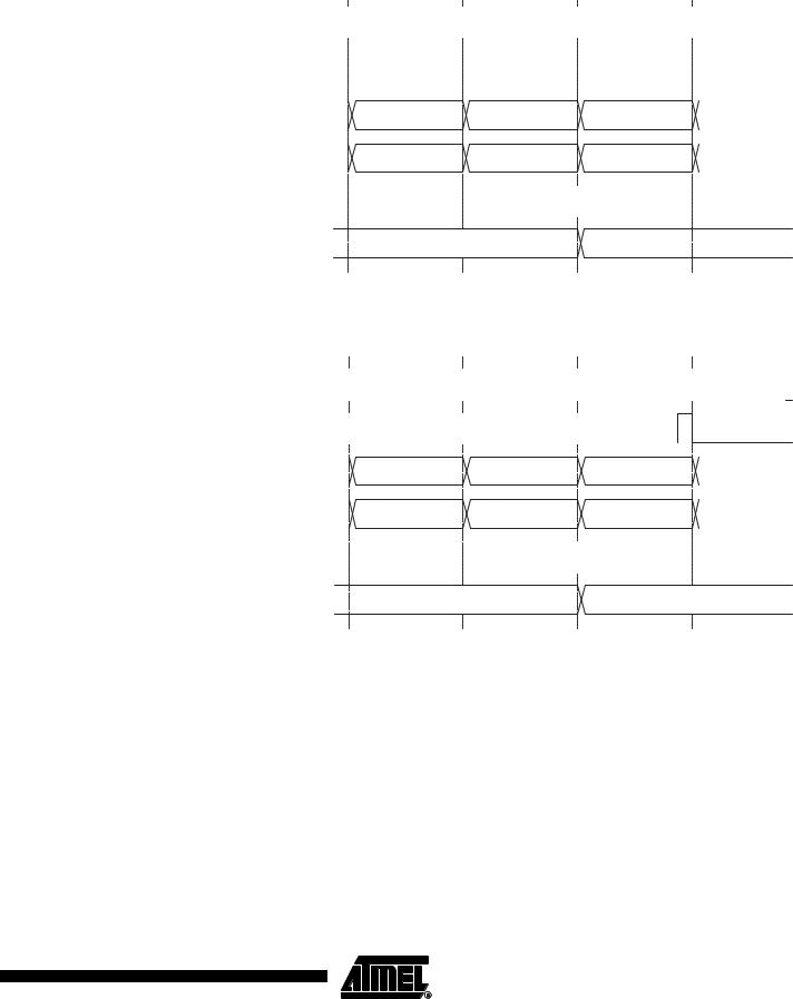
PWM Mode rect PWM mode (WGM13:0 = 8 or 9) provides a high resolution phase and frequency correct PWM waveform generation option. The phase and frequency correct PWM mode is, like the phase correct PWM mode, based on a dual-slope operation. The counter counts repeatedly from BOTTOM (0x0000) to TOP and then from TOP to BOTTOM. In non-inverting Compare Output mode, the Output Compare (OC1x) is cleared on the Compare Match between TCNT1 and OCR1x while upcounting, and set on the Compare Match while downcounting. In inverting Compare Output mode, the operation is inverted. The dual-slope operation gives a lower maximum operation frequency compared to the single-slope operation. However, due to the symmetric feature of the dualslope PWM modes, these modes are preferred for motor control applications.
The main difference between the phase correct, and the phase and frequency correct PWM mode is the time the OCR1x Register is updated by the OCR1x Buffer Register, (see Figure 54 and Figure 55).
The PWM resolution for the phase and frequency correct PWM mode can be defined by either ICR1 or OCR1A. The minimum resolution allowed is 2-bit (ICR1 or OCR1A set to 0x0003), and the maximum resolution is 16-bit (ICR1 or OCR1A set to MAX). The PWM resolution in bits can be calculated using the following equation:
RPFCPWM = |
log(TOP + 1) |
----------------------------------log(2) |
In phase and frequency correct PWM mode the counter is incremented until the counter value matches either the value in ICR1 (WGM13:0 = 8), or the value in OCR1A (WGM13:0 = 9). The counter has then reached the TOP and changes the count direction. The TCNT1 value will be equal to TOP for one timer clock cycle. The timing diagram for the phase correct and frequency correct PWM mode is shown on Figure 55. The figure shows phase and frequency correct PWM mode when OCR1A or ICR1 is used to define TOP. The TCNT1 value is in the timing diagram shown as a histogram for illustrating the dual-slope operation. The diagram includes non-inverted and inverted PWM outputs. The small horizontal line marks on the TCNT1 slopes represent Compare Matches between OCR1x and TCNT1. The OC1x Interrupt Flag will be set when a Compare Match occurs.
Figure 55. Phase and Frequency Correct PWM Mode, Timing Diagram
|
|
|
|
|
|
|
|
|
|
|
|
|
|
|
|
|
|
|
|
|
|
|
|
|
|
|
|
|
|
OCnA Interrupt Flag Set |
|
|
|
|
|
|
|
|
|
|
|
|
|
|
|
|
|
|
|
|
|
|
|
|
|
|
|
|
|
|
|
or ICFn Interrupt Flag Set |
|
|
|
|
|
|
|
|
|
|
|
|
|
|
|
|
|
|
|
|
|
|
|
|
|
|
|
|
|
|
|
(Interrupt on TOP) |
|
|
|
|
|
|
|
|
|
|
|
|
|
|
|
|
|
|
|
|
|
|
|
|
|
|
|
|
|
|
|
|
|
|
|
|
|
|
|
|
|
|
|
|
|
|
|
|
|
|
|
|
|
|
|
|
|
|
|
|
|
|
|
|
|
|
|
|
|
|
|
|
|
|
|
|
|
|
|
|
|
|
|
|
|
|
|
|
|
|
|
|
|
|
|
OCRnx/TOP Update and |
|
|
|
|
|
|
|
|
|
|
|
|
|
|
|
|
|
|
|
|
|
|
|
|
|
|
|
|
|
|
|
TOVn Interrupt Flag Set |
|
|
|
|
|
|
|
|
|
|
|
|
|
|
|
|
|
|
|
|
|
|
|
|
|
|
|
|
|
|
|
(Interrupt on Bottom) |
|
|
|
TCNTn |
|
|
|
|
|
|
|
|
|
|
|
|
|
|
|
|
|
|
|
|
|
|
|
|
|
|
|
||
|
|
|
|
|
|
|
|
|
|
|
|
|
|
|
|
|
|
|
|
|
|
|
|
|
|
|
|
|
|||
|
|
OCnx |
|
|
|
|
|
|
|
|
|
|
|
|
|
|
|
|
|
|
|
|
|
|
|
|
|
(COMnx1:0 = 2) |
|||
|
|
|
|
|
|
|
|
|
|
|
|
|
|
|
|
|
|
|
|
|
|
|
|
|
|
|
|||||
|
|
|
|
|
|
|
|
|
|
|
|
|
|
|
|
|
|
|
|
|
|
|
|
|
|
|
|
|
|
|
|
|
|
|
|
|
|
|
|
|
|
|
|
|
|
|
|
|
|
|
|
|
|
|
|
|
|
|
|
|
|
|
|
|
|
OCnx |
|
|
|
|
|
|
|
|
|
|
|
|
|
|
|
|
|
|
|
|
|
|
|
|
|
(COMnx1:0 = 3) |
|||
|
|
|
|
|
|
|
|
|
|
|
|
|
|
|
|
|
|
|
|
|
|
|
|
|
|
|
|
|
|
|
|
|
|
|
|
|
|
|
|
|
|
|
|
|
|
|
|
|
|
|
|
|
|
|
|
|
|
|
|
|
|||
|
|
Period |
|
|
|
|
|
|
|
|
|
|
|
|
|
|
|
|
|
|
|
|
|
|
|
|
|
||||
|
|
|
1 |
|
|
|
|
|
2 |
|
|
|
|
|
3 |
|
|
|
4 |
|
|
|
|
|
|
||||||
|
|
|
|
|
|
|
|
|
|
|
|
|
|
|
|||||||||||||||||
114 |
ATmega8515(L) |
|
|
|
|
|
|
|
|
|
|
|
|
|
|
|
|
|
|
|
|
|
|
|
|
|
|
|
|
||
|
|
|
|
|
|
|
|
|
|
|
|
|
|
|
|
|
|
|
|
|
|
|
|
|
|
|
|
||||
|
|
|
|
|
|
|
|
|
|
|
|
|
|
|
|
|
|
|
|
|
|
|
|
|
|
|
|
||||
2512G–AVR–03/05

 ATmega8515(L)
The Timer/Counter Overflow Flag (TOV1) is set at the same timer clock cycle as the OCR1x Registers are updated with the double buffer value (at BOTTOM). When either OCR1A or ICR1 is used for defining the TOP value, the OC1A or ICF1 Flag set when TCNT1 has reached TOP. The Interrupt Flags can then be used to generate an interrupt each time the counter reaches the TOP or BOTTOM value.
When changing the TOP value the program must ensure that the new TOP value is higher or equal to the value of all of the compare registers. If the TOP value is lower than any of the compare registers, a Compare Match will never occur between the TCNT1 and the OCR1x.
As Figure 55 shows the output generated is, in contrast to the phase correct mode, symmetrical in all periods. Since the OCR1x Registers are updated at BOTTOM, the length of the rising and the falling slopes will always be equal. This gives symmetrical output pulses and is therefore frequency correct.
Using the ICR1 Register for defining TOP works well when using fixed TOP values. By using ICR1, the OCR1A Register is free to be used for generating a PWM output on OC1A. However, if the base PWM frequency is actively changed by changing the TOP value, using the OCR1A as TOP is clearly a better choice due to its double buffer feature.
In phase and frequency correct PWM mode, the compare units allow generation of PWM waveforms on the OC1x pins. Setting the COM1x1:0 bits to 2 will produce a noninverted PWM and an inverted PWM output can be generated by setting the COM1x1:0 to 3 (See Table 1 on page 119). The actual OC1x value will only be visible on the port pin if the data direction for the port pin is set as output (DDR_OC1x). The PWM waveform is generated by setting (or clearing) the OC1x Register at the Compare Match between OCR1x and TCNT1 when the counter increments, and clearing (or setting) the OC1x Register at Compare Match between OCR1x and TCNT1 when the counter decrements. The PWM frequency for the output when using phase and frequency correct PWM can be calculated by the following equation:
fOCnxPFCPWM = |
fclk_I/O |
2---------------------------N TOP |
The N variable represents the prescaler divider (1, 8, 64, 256, or 1024).
The extreme values for the OCR1x Register represents special cases when generating a PWM waveform output in the phase correct PWM mode. If the OCR1x is set equal to BOTTOM the output will be continuously low and if set equal to TOP the output will be set to high for non-inverted PWM mode. For inverted PWM the output will have the opposite logic values. If OCR1A is used to define the TOP value (WGM1 = 9) and COM1A1:0 = 1, the OC1A output will toggle with a 50% duty cycle.
115
2512G–AVR–03/05

Timer/Counter Timing
Diagrams
The Timer/Counter is a synchronous design and the timer clock (clkT1) is therefore shown as a clock enable signal in the following figures. The figures include information on when Interrupt Flags are set, and when the OCR1x Register is updated with the OCR1x buffer value (only for modes utilizing double buffering). Figure 56 shows a timing diagram for the setting of OCF1x.
Figure 56. Timer/Counter Timing Diagram, Setting of OCF1x, no Prescaling
clkI/O
clkTn
(clkI/O/1)
TCNTn |
|
OCRnx - 1 |
|
OCRnx |
|
OCRnx + 1 |
|
OCRnx + 2 |
OCRnx |
|
|
|
|
|
|
|
|
|
|
|
|
|
|
|
|
|
|
|
|
OCRnx Value |
|
|
|
||
|
|
|
|
|
|
|
|
|
OCFnx
Figure 57 shows the same timing data, but with the prescaler enabled.
Figure 57. Timer/Counter Timing Diagram, Setting of OCF1x, with Prescaler (fclk_I/O/8)
clkI/O
clkTn
(clkI/O/8)
TCNTn |
|
|
OCRnx - 1 |
|
OCRnx |
|
OCRnx + 1 |
|
|
OCRnx + 2 |
|
|
|
|
|
|
|
|
|
|
|
OCRnx |
|
|
|
|
|
|
|
|
|
|
|
|
|
OCRnx Value |
|
|
|
|
|||
|
|
|
|
|
|
|
|
|
|
|
OCFnx
Figure 58 shows the count sequence close to TOP in various modes. When using phase and frequency correct PWM mode the OCR1x Register is updated at BOTTOM. The timing diagrams will be the same, but TOP should be replaced by BOTTOM, TOP-1 by BOTTOM+1 and so on. The same renaming applies for modes that set the TOV1 Flag at BOTTOM.
116 ATmega8515(L)
2512G–AVR–03/05
 ATmega8515(L)
Figure 58. Timer/Counter Timing Diagram, No Prescaling
clkI/O |
|
|
|
|
|
|
|
|
|
|
|
|
|
|
|
|
|
|
|
|
|
|
|
|
|
|
|
|
|
|
|
|
|
|
|
|
|
|
|
|
|
|
|
|
|
|
|
|
|
|
|
|
|
|
|
|
|
|
|
|
|
|
clkTn |
|
|
|
|
|
|
|
|
|
|
|
|
|
|
|
|
|
|
||
(clkI/O/1) |
|
|
|
|
|
|
|
|
|
|
|
|
|
|
|
|
|
|
||
|
|
|
|
|
|
|
|
|
|
|
|
|
|
|
|
|
|
|
|
|
TCNTn |
TOP - 1 |
|
|
|
TOP |
|
|
|
|
BOTTOM |
|
|
|
BOTTOM + 1 |
||||||
(CTC and FPWM) |
|
|
|
|
|
|
|
|
||||||||||||
|
|
|
|
|
|
|
|
|
|
|
|
|
|
|
|
|
|
|||
|
|
|
|
|
|
|
|
|
|
|
|
|
|
|
|
|
|
|
|
|
|
|
|
|
|
|
|
|
|
|
|
|
|
|
|
|
|
|
|
|
|
TCNTn |
TOP - 1 |
|
|
|
TOP |
|
|
|
|
TOP - 1 |
|
|
|
TOP - 2 |
||||||
(PC and PFC PWM) |
|
|
|
|
|
|
|
|
|
|
|
|||||||||
|
|
|
|
|
|
|
|
|
|
|
|
|
|
|
|
|
|
|||
TOVn (FPWM) |
|
|
|
|
|
|
|
|
|
|
|
|
|
|
|
|
|
|
||
|
|
|
|
|
|
|
|
|
|
|
|
|
|
|
|
|
|
|||
and ICFn (if used |
|
|
|
|
|
|
|
|
|
|
|
|
|
|
|
|
|
|
||
as TOP) |
|
|
|
|
|
|
|
|
|
|
|
|
|
|
|
|
|
|
|
|
|
|
|
|
|
|
|
|
|
|
|
|
|
|
|
|
|
|
|
|
|
|
|
|
|
|
|
|
|
|
|
|
|
|
|
|
|
|
|
|
|
|
OCRnx |
|
|
Old OCRnx Value |
|
|
|
|
|
|
|
New OCRnx Value |
|||||||||
(Update at TOP) |
|
|
|
|
|
|
|
|
|
|||||||||||
|
|
|
|
|
|
|
|
|
|
|
|
|
|
|
|
|
|
|
||
Figure 59 shows the same timing data, but with the prescaler enabled.
Figure 59. Timer/Counter Timing Diagram, with Prescaler (fclk_I/O/8)
clkI/O |
|
|
|
|
|
|
|
|
|
|
|
|
|
|
|
|
|
|
|
|
|
|
|
|
|
|
|
|
|
|
|
|
|
|
|
|
|
|
|
|
|
|
|
|
|
|
|
|
|
|
|
|
|
|
|
|
|
|
|
|
|
|
|
|
clkTn |
|
|
|
|
|
|
|
|
|
|
|
|
|
|
|
|
|
|
|
|
|
|
|
|
|
|
|
|
|
|
|
|
|
|
|
|
|
|
|
|
|
|
|
|
|
|
|
|
|
|
|
|
|
|
|
|
|
|
|
|
|
|
|
|
|
|
|
|
|
|
|
|
|
|
|
|
|
|
|
|
|
|
|
|
|
|
|
|
|
|
|
|
|
|
|
|
|
|
|
|
|
|
|
|
|
|
|
|
|
|
|
|
|
|
|
|
|
|
|
|
|
|
|
|
|
|
|
|
|
(clkI/O/8) |
|
|
|
|
|
|
|
|
|
|
|
|
|
|
|
|
|
|
|
|
|
|
|
|
|
|
|
|
|
|
|
|
|
|
|
|
|
|
|
|
|
|
|
|
|
|
|
|
|
|
|
|
|
|
|
|
|
|
|
|
|
|
|
|
TCNTn |
|
|
|
|
|
|
|
|
|
|
|
|
|
|
|
|
|
|
|
|
|
|
|
|
|
|
|
|
|
|
|
|
|
|
|
|
|
|
|
|
|
|
|
|
|
|
|
|
|
|
|
|
|
|
|
|
|
|
|
|
|
|
|
|
|
|
|
|
|
|
|
|
TOP - 1 |
|
|
|
|
|
|
|
|
|
TOP |
|
|
|
|
|
|
|
|
BOTTOM |
|
|
|
|
|
BOTTOM + 1 |
|
||||||||||||||||||||||||||||||
(CTC and FPWM) |
|
|
|
|
|
|
|
|
|
|
|
|
|
|
|
|
|
|
|
|
|
|
|
|
||||||||||||||||||||||||||||||||||||||||
|
|
|
|
|
|
|
|
|
|
|
|
|
|
|
|
|
|
|
|
|
|
|
|
|
|
|
|
|
|
|
|
|
|
|
|
|
|
|
|
|
|
|
|
|
|
|
|
|
|
|
|
|
|
|
|
|
|
|
|
|
|
|
|
|
TCNTn |
|
|
|
|
|
|
|
|
|
|
|
|
|
|
|
|
|
|
|
|
|
|
|
|
|
|
|
|
|
|
|
|
|
|
|
|
|
|
|
|
|
|
|
|
|
|
|
|
|
|
|
|
|
|
|
|
|
|
|
|
|
|
|
|
|
|
|
|
|
|
|
|
TOP - 1 |
|
|
|
|
|
|
|
|
|
TOP |
|
|
|
|
|
|
|
|
TOP - 1 |
|
|
|
|
|
|
|
TOP - 2 |
|
||||||||||||||||||||||||||||
(PC and PFC PWM) |
|
|
|
|
|
|
|
|
|
|
|
|
|
|
|
|
|
|
|
|
|
|
|
|
|
|
||||||||||||||||||||||||||||||||||||||
|
|
|
|
|
|
|
|
|
|
|
|
|
|
|
|
|
|
|
|
|
|
|
|
|
|
|
|
|
|
|
|
|
|
|
|
|
|
|
|
|
|
|
|
|
|
|
|
|
|
|
|
|
|
|
|
|
|
|
|
|
|
|
|
|
TOVn (FPWM) |
|
|
|
|
|
|
|
|
|
|
|
|
|
|
|
|
|
|
|
|
|
|
|
|
|
|
|
|
|
|
|
|
|
|
|
|
|
|
|
|
|
|
|
|
|
|
|
|
|
|
|
|
|
|
|
|
|
|
|
|
|
|
|
|
|
|
|
|
|
|
|
|
|
|
|
|
|
|
|
|
|
|
|
|
|
|
|
|
|
|
|
|
|
|
|
|
|
|
|
|
|
|
|
|
|
|
|
|
|
|
|
|
|
|
|
|
|
|
|
|
|
|
|
|
|
|
|
|
|
|
|
|
|
|
|
|
|
|
|
|
|
|
|
|
|
|
|
|
|
|
|
|
|
|
|
|
|
|
|
|
|
|
|
|
|
|
|
|
|
|
|
|
|
|
|
|
|
|
|
|
|
|
|
|
|
|
|
|
|
|
|
|
|
|
and ICFn (if used |
|
|
|
|
|
|
|
|
|
|
|
|
|
|
|
|
|
|
|
|
|
|
|
|
|
|
|
|
|
|
|
|
|
|
|
|
|
|
|
|
|
|
|
|
|
|
|
|
|
|
|
|
|
|
|
|
|
|
|
|
|
|
|
|
as TOP) |
|
|
|
|
|
|
|
|
|
|
|
|
|
|
|
|
|
|
|
|
|
|
|
|
|
|
|
|
|
|
|
|
|
|
|
|
|
|
|
|
|
|
|
|
|
|
|
|
|
|
|
|
|
|
|
|
|
|
|
|
|
|
|
|
|
|
|
|
|
|
|
|
|
|
|
|
|
|
|
|
|
|
|
|
|
|
|
|
|
|
|
|
|
|
|
|
|
|
|
|
|
|
|
|
|
|
|
|
|
|
|
|
|
|
|
|
|
|
|
|
|
|
|
|
|
|
|
|
|
OCRnx |
|
|
|
|
|
|
|
|
|
|
|
|
|
|
|
|
|
|
|
|
|
|
|
|
|
|
|
|
|
|
|
|
|
|
|
|
|
|
|
|
|
|
|
|
|
|
|
|
|
|
|
|
|
|
|
|
|
|
|
|
|
|
|
|
|
|
|
|
|
|
|
|
|
|
|
Old OCRnx Value |
|
|
|
|
|
|
|
|
|
|
|
|
|
|
|
|
|
|
|
|
|
New OCRnx Value |
|
||||||||||||||||||||||||||||||
(Update at TOP) |
|
|
|
|
|
|
|
|
|
|
|
|
|
|
|
|
|
|
|
|
|
|
|
|
|
|
|
|
|
|
|
|
|
|||||||||||||||||||||||||||||||
|
|
|
|
|
|
|
|
|
|
|
|
|
|
|
|
|
|
|
|
|
|
|
|
|
|
|
|
|
|
|
|
|
|
|
|
|
|
|
|
|
|
|
|
|
|
|
|
|
|
|
|
|
|
|
|
|
|
|
|
|
|
|
|
|
|
|
|
|
|
|
|
|
|
|
|
|
|
|
|
|
|
|
|
|
|
|
|
|
|
|
|
|
|
|
|
|
|
|
|
|
|
|
|
|
|
|
|
|
|
|
|
|
|
|
|
|
|
|
|
|
|
|
|
|
|
|
|
|
|
117
2512G–AVR–03/05

16-bit Timer/Counter
Register Description
Timer/Counter1 Control
Register A – TCCR1A
|
|
|
|
|
|
|
|
|
|
|
|
|
|
|
|
|
|
|
|
|
|
|
|
|
|
Bit |
7 |
6 |
5 |
4 |
3 |
2 |
1 |
0 |
|
|||
|
|
|
|
|
|
|
|
|
|
|||
|
COM1A1 |
COM1A0 |
COM1B1 |
COM1B0 |
FOC1A |
FOC1B |
WGM11 |
WGM10 |
TCCR1A |
|||
|
|
|
|
|
|
|
|
|
|
|
|
|
Read/Write |
R/W |
R/W |
|
|
R/W |
R/W |
W |
W |
R/W |
R/W |
||
Initial Value |
0 |
0 |
0 |
0 |
0 |
0 |
0 |
0 |
|
|||
•Bit 7:6 – COM1A1:0: Compare Output Mode for Channel A
•Bit 5:4 – COM1B1:0: Compare Output Mode for Channel B
The COM1A1:0 and COM1B1:0 control the Output Compare pins (OC1A and OC1B respectively) behavior. If one or both of the COM1A1:0 bits are written to one, the OC1A output overrides the normal port functionality of the I/O pin it is connected to. If one or both of the COM1B1:0 bit are written to one, the OC1B output overrides the normal port functionality of the I/O pin it is connected to. However, note that the Data Direction Register (DDR) bit corresponding to the OC1A or OC1B pin must be set in order to enable the output driver.
When the OC1A or OC1B is connected to the pin, the function of the COM1x1:0 bits is dependent of the WGM13:0 bits setting. Table 50 shows the COM1x1:0 bit functionality when the WGM13:0 bits are set to a normal or a CTC mode (non-PWM).
Table 50. Compare Output Mode, non-PWM
COM1A1/ |
COM1A0/ |
|
COM1B1 |
COM1B0 |
Description |
|
|
|
0 |
0 |
Normal port operation, OC1A/OC1B disconnected. |
|
|
|
0 |
1 |
Toggle OC1A/OC1B on Compare Match. |
|
|
|
1 |
0 |
Clear OC1A/OC1B on Compare Match (Set output to low level). |
|
|
|
1 |
1 |
Set OC1A/OC1B on Compare Match (Set output to high level). |
|
|
|
Table 51 shows the COM1x1:0 bit functionality when the WGM13:0 bits are set to the fast PWM mode.
Table 51. Compare Output Mode, Fast PWM(1)
COM1A1/ |
COM1A0/ |
|
COM1B1 |
COM1B0 |
Description |
|
|
|
0 |
0 |
Normal port operation, OC1A/OC1B disconnected. |
|
|
|
0 |
1 |
WGM13:0 = 15: Toggle OC1A on Compare Match, OC1B |
|
|
disconnected (Normal port operation). For all other WGM1 |
|
|
setting, Normal port operation, OC1A/OC1B disconnected. |
|
|
|
1 |
0 |
Clear OC1A/OC1B on Compare Match, set OC1A/OC1B at TOP. |
|
|
|
1 |
1 |
Set OC1A/OC1B on Compare Match, clear OC1A/OC1B at TOP. |
|
|
|
Note: 1. A special case occurs when OCR1A/OCR1B equals TOP and COM1A1/COM1B1 is set. In this case the Compare Match is ignored, but the set or clear is done at TOP. See “Fast PWM Mode” on page 110. for more details.
Table 52 shows the COM1x1:0 bit functionality when the WGM13:0 bits are set to the phase correct or the phase and frequency correct, PWM mode.
118 ATmega8515(L)
2512G–AVR–03/05

 ATmega8515(L)
Table 52. Compare Output Mode, Phase Correct and Phase and Frequency Correct
PWM(1)
COM1A1/ |
COM1A0/ |
|
COM1B1 |
COM1B0 |
Description |
|
|
|
0 |
0 |
Normal port operation, OC1A/OC1B disconnected. |
|
|
|
0 |
1 |
WGM13:0 = 9 or 14: Toggle OC1A on Compare Match, OC1B |
|
|
disconnected (Normal port operation). For all other WGM1 |
|
|
setting, Normal port operation, OC1A/OC1B disconnected. |
|
|
|
1 |
0 |
Clear OC1A/OC1B on Compare Match when up-counting. Set |
|
|
OC1A/OC1B on Compare Match when downcounting. |
11 Set OC1A/OC1B on Compare Match when up-counting. Clear OC1A/OC1B on Compare Match when downcounting.
Note: 1. A special case occurs when OCR1A/OCR1B equals TOP and COM1A1/COM1B1 is set. See “Phase Correct PWM Mode” on page 112. for more details.
•Bit 3 – FOC1A: Force Output Compare for Channel A
•Bit 2 – FOC1B: Force Output Compare for Channel B
The FOC1A/FOC1B bits are only active when the WGM13:0 bits specifies a non-PWM mode. However, for ensuring compatibility with future devices, these bits must be set to zero when TCCR1A is written when operating in a PWM mode. When writing a logical one to the FOC1A/FOC1B bit, an immediate Compare Match is forced on the waveform generation unit. The OC1A/OC1B output is changed according to its COM1x1:0 bits setting. Note that the FOC1A/FOC1B bits are implemented as strobes. Therefore it is the value present in the COM1x1:0 bits that determine the effect of the forced compare.
A FOC1A/FOC1B strobe will not generate any interrupt nor will it clear the timer in Clear
Timer on Compare Match (CTC) mode using OCR1A as TOP.
The FOC1A/FOC1B bits are always read as zero.
• Bit 1:0 – WGM11:0: Waveform Generation Mode
Combined with the WGM13:2 bits found in the TCCR1B Register, these bits control the counting sequence of the counter, the source for maximum (TOP) counter value, and what type of waveform generation to be used, see Table 53. Modes of operation supported by the Timer/Counter unit are: Normal mode (counter), Clear Timer on Compare Match (CTC) mode, and three types of Pulse Width Modulation (PWM) modes. See “Modes of Operation” on page 108.
119
2512G–AVR–03/05

Table 53. Waveform Generation Mode Bit Description(1)
|
|
WGM12 |
WGM11 |
WGM10 |
|
|
Update of |
TOV1 Flag |
Mode |
WGM13 |
(CTC1) |
(PWM11) |
(PWM10) |
Timer/Counter Mode of Operation |
TOP |
OCR1x at |
Set on |
|
|
|
|
|
|
|
|
|
0 |
0 |
0 |
0 |
0 |
Normal |
0xFFFF |
Immediate |
MAX |
|
|
|
|
|
|
|
|
|
1 |
0 |
0 |
0 |
1 |
PWM, Phase Correct, 8-bit |
0x00FF |
TOP |
BOTTOM |
|
|
|
|
|
|
|
|
|
2 |
0 |
0 |
1 |
0 |
PWM, Phase Correct, 9-bit |
0x01FF |
TOP |
BOTTOM |
|
|
|
|
|
|
|
|
|
3 |
0 |
0 |
1 |
1 |
PWM, Phase Correct, 10-bit |
0x03FF |
TOP |
BOTTOM |
|
|
|
|
|
|
|
|
|
4 |
0 |
1 |
0 |
0 |
CTC |
OCR1A |
Immediate |
MAX |
|
|
|
|
|
|
|
|
|
5 |
0 |
1 |
0 |
1 |
Fast PWM, 8-bit |
0x00FF |
TOP |
TOP |
|
|
|
|
|
|
|
|
|
6 |
0 |
1 |
1 |
0 |
Fast PWM, 9-bit |
0x01FF |
TOP |
TOP |
|
|
|
|
|
|
|
|
|
7 |
0 |
1 |
1 |
1 |
Fast PWM, 10-bit |
0x03FF |
TOP |
TOP |
|
|
|
|
|
|
|
|
|
8 |
1 |
0 |
0 |
0 |
PWM, Phase and Frequency Correct |
ICR1 |
BOTTOM |
BOTTOM |
|
|
|
|
|
|
|
|
|
9 |
1 |
0 |
0 |
1 |
PWM, Phase and Frequency Correct |
OCR1A |
BOTTOM |
BOTTOM |
|
|
|
|
|
|
|
|
|
10 |
1 |
0 |
1 |
0 |
PWM, Phase Correct |
ICR1 |
TOP |
BOTTOM |
|
|
|
|
|
|
|
|
|
11 |
1 |
0 |
1 |
1 |
PWM, Phase Correct |
OCR1A |
TOP |
BOTTOM |
|
|
|
|
|
|
|
|
|
12 |
1 |
1 |
0 |
0 |
CTC |
ICR1 |
Immediate |
MAX |
|
|
|
|
|
|
|
|
|
13 |
1 |
1 |
0 |
1 |
Reserved |
– |
– |
– |
|
|
|
|
|
|
|
|
|
14 |
1 |
1 |
1 |
0 |
Fast PWM |
ICR1 |
TOP |
TOP |
|
|
|
|
|
|
|
|
|
15 |
1 |
1 |
1 |
1 |
Fast PWM |
OCR1A |
TOP |
TOP |
|
|
|
|
|
|
|
|
|
Note: 1. The CTC1 and PWM11:0 bit definition names are obsolete. Use the WGM12:0 definitions. However, the functionality and location of these bits are compatible with previous versions of the timer.
120 ATmega8515(L)
2512G–AVR–03/05
Timer/Counter1 Control
Register B – TCCR1B
2512G–AVR–03/05
ATmega8515(L)
Bit |
7 |
6 |
5 |
4 |
3 |
2 |
1 |
0 |
|
|
ICNC1 |
ICES1 |
– |
WGM13 |
WGM12 |
CS12 |
CS11 |
CS10 |
TCCR1B |
|
|
|
|
|
|
|
|
|
|
Read/Write |
R/W |
R/W |
R |
R/W |
R/W |
R/W |
R/W |
R/W |
|
Initial Value |
0 |
0 |
0 |
0 |
0 |
0 |
0 |
0 |
|
• Bit 7 – ICNC1: Input Capture Noise Canceler
Setting this bit (to one) activates the Input Capture Noise Canceler. When the Noise Canceler is activated, the input from the Input Capture Pin (ICP1) is filtered. The filter function requires four successive equal valued samples of the ICP1 pin for changing its output. The Input Capture is therefore delayed by four Oscillator cycles when the noise canceler is enabled.
• Bit 6 – ICES1: Input Capture Edge Select
This bit selects which edge on the Input Capture Pin (ICP1) that is used to trigger a capture event. When the ICES1 bit is written to zero, a falling (negative) edge is used as trigger, and when the ICES1 bit is written to one, a rising (positive) edge will trigger the capture.
When a capture is triggered according to the ICES1 setting, the counter value is copied into the Input Capture Register (ICR1). The event will also set the Input Capture Flag (ICF1), and this can be used to cause an Input Capture Interrupt, if this interrupt is enabled.
When the ICR1 is used as TOP value (see description of the WGM13:0 bits located in the TCCR1A and the TCCR1B Register), the ICP1 is disconnected and consequently the Input Capture function is disabled.
• Bit 5: Reserved Bit
This bit is reserved for future use. For ensuring compatibility with future devices, this bit must be written to zero when TCCR1B is written.
• Bit 4:3 – WGM13:2: Waveform Generation Mode
See TCCR1A Register description.
• Bit 2:0 – CS12:0: Clock Select
The three Clock Select bits select the clock source to be used by the Timer/Counter, see Figure 56 and Figure 57.
Table 54. Clock Select Bit Description
CS12 |
CS11 |
CS10 |
Description |
|
|
|
|
0 |
0 |
0 |
No clock source (Timer/counter stopped). |
|
|
|
|
0 |
0 |
1 |
clkI/O/1 (No prescaling) |
|
|
|
|
0 |
1 |
0 |
clkI/O/8 (From prescaler) |
0 |
1 |
1 |
clkI/O/64 (From prescaler) |
|
|
|
|
1 |
0 |
0 |
clkI/O/256 (From prescaler) |
|
|
|
|
1 |
0 |
1 |
clkI/O/1024 (From prescaler) |
1 |
1 |
0 |
External clock source on T1 pin. Clock on falling edge. |
|
|
|
|
1 |
1 |
1 |
External clock source on T1 pin. Clock on rising edge. |
|
|
|
|
If external pin modes are used for the Timer/Counter1, transitions on the T1 pin will clock the counter even if the pin is configured as an output. This feature allows software control of the counting.
121

Timer/Counter1 – TCNT1H
and TCNT1L
|
|
|
|
|
|
|
|
|
|
|
|
|
|
|
|
|
|
|
|
|
|
|
|
Bit |
7 |
6 |
5 |
4 |
3 |
2 |
1 |
0 |
|
||
|
|
|
|
|
|
|
|
|
|
|
|
|
|
|
|
|
|
TCNT1[15:8] |
|
|
|
TCNT1H |
|
|
|
|
|
|
|
|
|
|
|
|
|
|
|
|
|
|
|
TCNT1[7:0] |
|
|
|
TCNT1L |
|
|
|
|
|
|
|
|
|
|
|
|
|
Read/Write |
R/W |
R/W |
|
R/W |
R/W |
R/W |
R/W |
R/W |
R/W |
||
Initial Value |
0 |
0 |
0 |
0 |
0 |
0 |
0 |
0 |
|
||
The two Timer/Counter I/O locations (TCNT1H and TCNT1L, combined TCNT1) give direct access, both for read and for write operations, to the Timer/Counter unit 16-bit counter. To ensure that both the high and low bytes are read and written simultaneously when the CPU accesses these registers, the access is performed using an 8-bit temporary High Byte Register (TEMP). This temporary register is shared by all the other 16-bit registers. See “Accessing 16-bit Registers” on page 99.
Modifying the counter (TCNT1) while the counter is running introduces a risk of missing a Compare Match between TCNT1 and one of the OCR1x Registers.
Writing to the TCNT1 Register blocks (removes) the Compare Match on the following timer clock for all compare units.
Output Compare Register 1 A
– OCR1AH and OCR1AL
Output Compare Register 1 B
– OCR1BH and OCR1BL
Bit |
7 |
6 |
5 |
4 |
3 |
2 |
1 |
0 |
|
|
|
|
|
OCR1A[15:8] |
|
|
|
OCR1AH |
|
|
|
|
|
|
|
|
|
|
|
|
|
|
|
OCR1A[7:0] |
|
|
|
OCR1AL |
|
|
|
|
|
|
|
|
|
|
|
Read/Write |
R/W |
R/W |
R/W |
R/W |
R/W |
R/W |
R/W |
R/W |
|
Initial Value |
0 |
0 |
0 |
0 |
0 |
0 |
0 |
0 |
|
Bit |
7 |
6 |
5 |
4 |
3 |
2 |
1 |
0 |
|
|
|
|
|
|
|
|
|
|
|
|
|
|
|
OCR1B[15:8] |
|
|
|
OCR1BH |
|
|
|
|
|
|
|
|
|
|
|
|
|
|
|
OCR1B[7:0] |
|
|
|
OCR1BL |
|
|
|
|
|
|
|
|
|
|
|
Read/Write |
R/W |
R/W |
R/W |
R/W |
R/W |
R/W |
R/W |
R/W |
|
Initial Value |
0 |
0 |
0 |
0 |
0 |
0 |
0 |
0 |
|
The Output Compare Registers contain a 16-bit value that is continuously compared with the counter value (TCNT1). A match can be used to generate an output compare interrupt, or to generate a waveform output on the OC1x pin.
The Output Compare Registers are 16-bit in size. To ensure that both the high and low bytes are written simultaneously when the CPU writes to these registers, the access is performed using an 8-bit temporary High Byte Register (TEMP). This temporary register is shared by all the other 16-bit registers. See “Accessing 16-bit Registers” on page 99.
122 ATmega8515(L)
2512G–AVR–03/05

 ATmega8515(L)
Input Capture Register 1 –
ICR1H and ICR1L
Bit |
7 |
6 |
5 |
4 |
3 |
2 |
1 |
0 |
|
|
|
|
|
ICR1[15:8] |
|
|
|
ICR1H |
|
|
|
|
|
|
|
|
|
|
|
|
|
|
|
ICR1[7:0] |
|
|
|
ICR1L |
|
|
|
|
|
|
|
|
|
|
|
Read/Write |
R/W |
R/W |
R/W |
R/W |
R/W |
R/W |
R/W |
R/W |
|
Initial Value |
0 |
0 |
0 |
0 |
0 |
0 |
0 |
0 |
|
The Input Capture is updated with the counter (TCNT1) value each time an event occurs on the ICP1 pin (or optionally on the Analog Comparator output for Timer/Counter1). The Input Capture can be used for defining the counter TOP value.
The Input Capture Register is 16-bit in size. To ensure that both the high and low bytes are read simultaneously when the CPU accesses these registers, the access is performed using an 8-bit temporary High Byte Register (TEMP). This temporary register is shared by all the other 16-bit registers. See “Accessing 16-bit Registers” on page 99.
Timer/Counter Interrupt Mask
Register – TIMSK(1)
2512G–AVR–03/05
Bit |
7 |
6 |
5 |
4 |
3 |
2 |
1 |
0 |
|
|
TOIE1 |
OCIE1A |
OCIE1B |
OCIE2 |
TICIE1 |
TOIE2 |
TOIE0 |
OCIE0 |
TIMSK |
Read/Write |
R/W |
R/W |
R/W |
R/W |
R/W |
R/W |
R/W |
R/W |
|
Initial Value |
0 |
0 |
0 |
0 |
0 |
0 |
0 |
0 |
|
Note: 1. This register contains interrupt control bits for several Timer/Counters, but only Timer1 bits are described in this section. The remaining bits are described in their respective timer sections.
• Bit 7 – TOIE1: Timer/Counter1, Overflow Interrupt Enable
When this bit is written to one, and the I-flag in the Status Register is set (interrupts globally enabled), the Timer/Counter1 overflow interrupt is enabled. The corresponding Interrupt Vector (see “Interrupts” on page 53) is executed when the TOV1 Flag, located in TIFR, is set.
• Bit 6 – OCIE1A: Timer/Counter1, Output Compare A Match Interrupt Enable
When this bit is written to one, and the I-flag in the Status Register is set (interrupts globally enabled), the Timer/Counter1 Output Compare A Match interrupt is enabled. The corresponding Interrupt Vector (see “Interrupts” on page 53) is executed when the OCF1A Flag, located in TIFR, is set.
• Bit 5 – OCIE1B: Timer/Counter1, Output Compare B Match Interrupt Enable
When this bit is written to one, and the I-flag in the Status Register is set (interrupts globally enabled), the Timer/Counter1 Output Compare B Match interrupt is enabled. The corresponding Interrupt Vector (see “Interrupts” on page 53) is executed when the OCF1B Flag, located in TIFR, is set.
• Bit 3 – TICIE1: Timer/Counter1, Input Capture Interrupt Enable
When this bit is written to one, and the I-flag in the Status Register is set (interrupts globally enabled), the Timer/Counter1 Input Capture interrupt is enabled. The corresponding Interrupt Vector (see “Interrupts” on page 53) is executed when the ICF1 Flag, located in TIFR, is set.
123

Timer/Counter Interrupt Flag
Register – TIFR(1)
|
|
|
|
|
|
|
|
|
|
|
|
|
|
|
|
|
|
|
|
|
|
|
|
|
|
Bit |
7 |
6 |
|
5 |
4 |
3 |
2 |
1 |
0 |
|
||
|
|
|
|
|
|
|
|
|
|
|
||
|
TOV1 |
OCF1A |
|
OC1FB |
– |
ICF1 |
– |
TOV0 |
OCF0 |
TIFR |
||
Read/Write |
R/W |
R/W |
|
R/W |
R/W |
R/W |
R/W |
R/W |
R/W |
|
||
Initial Value |
0 |
0 |
|
0 |
0 |
0 |
0 |
0 |
0 |
|
||
Note: 1. This register contains flag bits for several Timer/Counters, but only Timer1 bits are described in this section. The remaining bits are described in their respective timer sections.
• Bit 7 – TOV1: Timer/Counter1, Overflow Flag
The setting of this flag is dependent of the WGM13:0 bits setting. In Normal and CTC modes, the TOV1 Flag is set when the timer overflows. Refer to Table 53 on page 120 for the TOV1 Flag behavior when using another WGM13:0 bit setting.
TOV1 is automatically cleared when the Timer/Counter1 Overflow Interrupt Vector is executed. Alternatively, TOV1 can be cleared by writing a logic one to its bit location.
• Bit 6 – OCF1A: Timer/Counter1, Output Compare A Match Flag
This flag is set in the timer clock cycle after the counter (TCNT1) value matches the Output Compare Register A (OCR1A).
Note that a Forced Output Compare (FOC1A) strobe will not set the OCF1A Flag.
OCF1A is automatically cleared when the Output Compare Match A Interrupt Vector is executed. Alternatively, OCF1A can be cleared by writing a logic one to its bit location.
• Bit 5 – OCF1B: Timer/Counter1, Output Compare B Match Flag
This flag is set in the timer clock cycle after the counter (TCNT1) value matches the Output Compare Register B (OCR1B).
Note that a Forced Output Compare (FOC1B) strobe will not set the OCF1B Flag.
OCF1B is automatically cleared when the Output Compare Match B Interrupt vector is executed. Alternatively, OCF1B can be cleared by writing a logic one to its bit location.
• Bit 3 – ICF1: Timer/Counter1, Input Capture Flag
This flag is set when a capture event occurs on the ICP1 pin. When the Input Capture Register (ICR1) is set by the WGM13:0 to be used as the TOP value, the ICF1 Flag is set when the counter reaches the TOP value.
ICF1 is automatically cleared when the Input Capture Interrupt Vector is executed. Alternatively, ICF1 can be cleared by writing a logic one to its bit location.
124 ATmega8515(L)
2512G–AVR–03/05
 ATmega8515(L)
Serial Peripheral
Interface – SPI
The Serial Peripheral Interface (SPI) allows high-speed synchronous data transfer between the ATmega8515 and peripheral devices or between several AVR devices. The ATmega8515 SPI includes the following features:
•Full Duplex, 3-wire Synchronous Data Transfer
•Master or Slave Operation
•LSB First or MSB First Data Transfer
•Seven Programmable Bit Rates
•End of Transmission Interrupt Flag
•Write Collision Flag Protection
•Wake-up from Idle Mode
•Double Speed (CK/2) Master SPI Mode
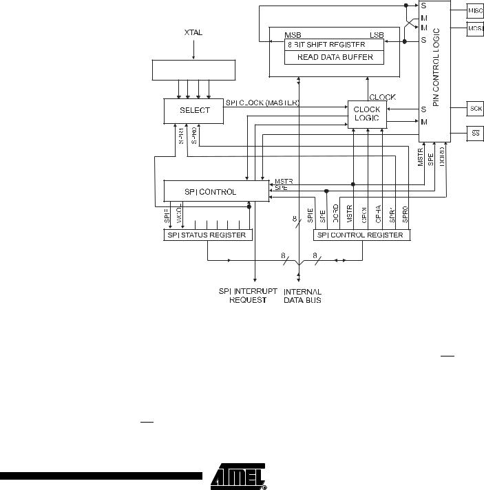
Figure 60. SPI Block Diagram(1)
DIVIDER |
/2/4/8/16/32/64/128 |
SPI2X |
SPI2X |
Note: 1. Refer to Figure 1 on page 2, and Table 29 on page 66 for SPI pin placement.
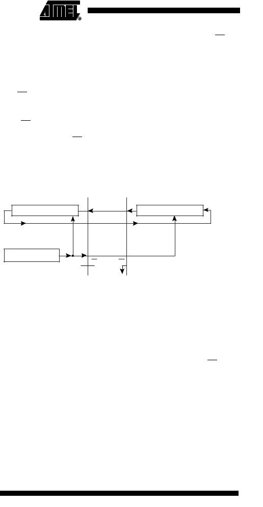
The interconnection between Master and Slave CPUs with SPI is shown in Figure 61. The system consists of two Shift Registers, and a Master clock generator. The SPI Master initiates the communication cycle when pulling low the Slave Select SS pin of the desired Slave. Master and Slave prepare the data to be sent in their respective Shift Registers, and the Master generates the required clock pulses on the SCK line to interchange data. Data is always shifted from Master to Slave on the Master Out – Slave In, MOSI, line, and from Slave to Master on the Master In – Slave Out, MISO, line. After each data packet, the Master will synchronize the Slave by pulling high the Slave Select, SS, line.
125
2512G–AVR–03/05
When configured as a Master, the SPI interface has no automatic control of the SS line. This must be handled by user software before communication can start. When this is done, writing a byte to the SPI Data Register starts the SPI clock generator, and the hardware shifts the 8 bits into the Slave. After shifting one byte, the SPI clock generator stops, setting the end of Transmission Flag (SPIF). If the SPI Interrupt Enable bit (SPIE) in the SPCR Register is set, an interrupt is requested. The Master may continue to shift the next byte by writing it into SPDR, or signal the end of packet by pulling high the Slave Select, SS line. The last incoming byte will be kept in the Buffer Register for later use.
When configured as a Slave, the SPI interface will remain sleeping with MISO tri-stated as long as the SS pin is driven high. In this state, software may update the contents of the SPI Data Register, SPDR, but the data will not be shifted out by incoming clock pulses on the SCK pin until the SS pin is driven low. As one byte has been completely shifted, the end of Transmission Flag, SPIF is set. If the SPI Interrupt Enable bit, SPIE, in the SPCR Register is set, an interrupt is requested. The Slave may continue to place new data to be sent into SPDR before reading the incoming data. The last incoming byte will be kept in the Buffer Register for later use.
Figure 61. SPI Master-Slave Interconnection
MSB |
MASTER |
LSB |
MSB |
SLAVE |
LSB |
|
|
MISO |
MISO |
|
|
8-BIT SHIFT REGISTER |
8-BIT SHIFT REGISTER |
||||
|
|
MOSI |
MOSI |
|
|
|
|
|
|
|
SHIFT |
|
|
|
|
|
ENABLE |
|
SPI |
SCK |
SCK |
|
|
CLOCK GENERATOR |
SS |
SS |
|
|
|
|
|
|
|
||
|
|
VCC |
|
|
|
The system is single buffered in the transmit direction and double buffered in the receive direction. This means that bytes to be transmitted cannot be written to the SPI Data Register before the entire shift cycle is completed. When receiving data, however, a received character must be read from the SPI Data Register before the next character has been completely shifted in. Otherwise, the first byte is lost.
In SPI Slave mode, the control logic will sample the incoming signal of the SCK pin. To ensure correct sampling of the clock signal, the frequency of the SPI clock should never exceed fosc/4.
When the SPI is enabled, the data direction of the MOSI, MISO, SCK, and SS pins is overridden according to Table 55. For more details on automatic port overrides, refer to “Alternate Port Functions” on page 63.
Table 55. SPI Pin Overrides(1)
Pin |
Direction, Master SPI |
Direction, Slave SPI |
||
|
|
|
||
MOSI |
User Defined |
Input |
||
|
|
|
||
MISO |
Input |
User Defined |
||
|
|
|
||
SCK |
User Defined |
Input |
||
|
|
|
|
|
|
|
|
User Defined |
Input |
|
SS |
|||
|
|
|
|
|
Note: 1. See “Alternate Functions Of Port B” on page 66 for a detailed description of how to define the direction of the user defined SPI pins.
126 ATmega8515(L)
2512G–AVR–03/05

 ATmega8515(L)
The following code examples show how to initialize the SPI as a Master and how to perform a simple transmission. DDR_SPI in the examples must be replaced by the actual Data Direction Register controlling the SPI pins. DD_MOSI, DD_MISO and DD_SCK must be replaced by the actual data direction bits for these pins. For example, if MOSI is placed on pin PB5, replace DD_MOSI with DDB5 and DDR_SPI with DDRB.
Assembly Code Example(1)
SPI_MasterInit:
; Set MOSI and SCK output, all others input
ldi r17,(1<<DD_MOSI)|(1<<DD_SCK) out DDR_SPI,r17
; Enable SPI, Master, set clock rate fck/16 ldi r17,(1<<SPE)|(1<<MSTR)|(1<<SPR0)
out SPCR,r17 ret
SPI_MasterTransmit:
; Start transmission of data (r16) out SPDR,r16
Wait_Transmit:
; Wait for transmission complete sbis SPSR,SPIF
rjmp Wait_Transmit
ret
C Code Example(1)
void SPI_MasterInit(void)
{
/* Set MOSI and SCK output, all others input */ DDR_SPI = (1<<DD_MOSI)|(1<<DD_SCK);
/* Enable SPI, Master, set clock rate fck/16 */ SPCR = (1<<SPE)|(1<<MSTR)|(1<<SPR0);
}
void SPI_MasterTransmit(char cData)
{
/* Start transmission */ SPDR = cData;
/* Wait for transmission complete */ while(!(SPSR & (1<<SPIF)))
;
}
Note: 1. See “About Code Examples” on page 6.
127
2512G–AVR–03/05

The following code examples show how to initialize the SPI as a Slave and how to perform a simple reception.
Assembly Code Example(1)
SPI_SlaveInit:
; Set MISO output, all others input
ldi |
r17,(1<<DD_MISO) |
out |
DDR_SPI,r17 |
; Enable SPI |
|
ldi |
r17,(1<<SPE) |
out |
SPCR,r17 |
ret |
|
SPI_SlaveReceive:
; Wait for reception complete sbis SPSR,SPIF
rjmp SPI_SlaveReceive
; Read received data and return in r16,SPDR
ret
C Code Example(1)
void SPI_SlaveInit(void)
{
/* Set MISO output, all others input */ DDR_SPI = (1<<DD_MISO);
/* Enable SPI */ SPCR = (1<<SPE);
}
char SPI_SlaveReceive(void)
{
/* Wait for reception complete */ while(!(SPSR & (1<<SPIF)))
;
/* Return data register */ return SPDR;
}
Note: 1. See “About Code Examples” on page 6.
128 ATmega8515(L)
2512G–AVR–03/05