- •Features
- •Pin Configurations
- •Overview
- •Block Diagram
- •Disclaimer
- •Pin Descriptions
- •Port A (PA7..PA0)
- •Port B (PB7..PB0)
- •Port C (PC7..PC0)
- •Port D (PD7..PD0)
- •Port E(PE2..PE0)
- •RESET
- •XTAL1
- •XTAL2
- •AVR CPU Core
- •Introduction
- •Architectural Overview
- •Status Register
- •Stack Pointer
- •Interrupt Response Time
- •In-System Reprogrammable Flash Program memory
- •SRAM Data Memory
- •Data Memory Access Times
- •EEPROM Data Memory
- •EEPROM Read/Write Access
- •I/O Memory
- •Overview
- •Address Latch Requirements
- •Pull-up and Bus Keeper
- •Timing
- •Using all Locations of External Memory Smaller than 64 KB
- •Using all 64KB Locations of External Memory
- •Clock Systems and their Distribution
- •Clock Sources
- •Default Clock Source
- •Crystal Oscillator
- •External RC Oscillator
- •External Clock
- •Idle Mode
- •Power-down Mode
- •Standby Mode
- •Analog Comparator
- •Brown-out Detector
- •Internal Voltage Reference
- •Watchdog Timer
- •Port Pins
- •Resetting the AVR
- •Reset Sources
- •Power-on Reset
- •External Reset
- •Brown-out Detection
- •Watchdog Reset
- •Watchdog Timer
- •Timed Sequences for Changing the Configuration of the Watchdog Timer
- •Safety Level 0
- •Safety Level 1
- •Safety Level 2
- •Interrupts
- •Moving Interrupts between Application and Boot Space
- •I/O Ports
- •Introduction
- •Configuring the Pin
- •Reading the Pin Value
- •Unconnected pins
- •Alternate Port Functions
- •Alternate Functions of Port A
- •Alternate Functions Of Port B
- •Alternate Functions of Port C
- •Alternate Functions of Port D
- •Alternate Functions of Port E
- •Register Description for I/O Ports
- •External Interrupts
- •8-bit Timer/Counter0 with PWM
- •Overview
- •Registers
- •Definitions
- •Counter Unit
- •Output Compare Unit
- •Force Output Compare
- •Modes of Operation
- •Normal Mode
- •Fast PWM Mode
- •Phase Correct PWM Mode
- •Internal Clock Source
- •Prescaler Reset
- •External Clock Source
- •16-bit Timer/Counter1
- •Overview
- •Registers
- •Definitions
- •Compatibility
- •Counter Unit
- •Input Capture Unit
- •Input Capture Trigger Source
- •Noise Canceler
- •Using the Input Capture Unit
- •Output Compare Units
- •Force Output Compare
- •Modes of Operation
- •Normal Mode
- •Fast PWM Mode
- •Phase Correct PWM Mode
- •Slave Mode
- •Master Mode
- •Data Modes
- •USART
- •Single USART
- •Clock Generation
- •External Clock
- •Synchronous Clock Operation
- •Frame Formats
- •Parity Bit Calculation
- •USART Initialization
- •Sending Frames with 5 to 8 Data Bits
- •Sending Frames with 9 Data Bits
- •Parity Generator
- •Disabling the Transmitter
- •Receiving Frames with 5 to 8 Data Bits
- •Receiving Frames with 9 Data Bits
- •Receiver Error Flags
- •Parity Checker
- •Disabling the Receiver
- •Flushing the Receive Buffer
- •Asynchronous Data Recovery
- •Using MPCM
- •Write Access
- •Read Access
- •Analog Comparator
- •Features
- •Application Section
- •Boot Loader Lock bits
- •Performing a Page Write
- •Using the SPM Interrupt
- •Setting the Boot Loader Lock bits by SPM
- •Reading the Fuse and Lock bits from Software
- •Preventing Flash Corruption
- •Simple Assembly Code Example for a Boot Loader
- •Program and Data Memory Lock bits
- •Fuse bits
- •Latching of Fuses
- •Signature Bytes
- •Calibration Byte
- •Calibration Byte
- •Signal Names
- •Parallel Programming
- •Enter Programming Mode
- •Chip Erase
- •Programming the Flash
- •Programming the EEPROM
- •Reading the Flash
- •Reading the EEPROM
- •Programming the Lock bits
- •Reading the Signature Bytes
- •Reading the Calibration Byte
- •Serial Downloading
- •Data Polling Flash
- •Data Polling EEPROM
- •Electrical Characteristics
- •Absolute Maximum Ratings*
- •External Clock Drive Waveforms
- •External Clock Drive
- •External Data Memory Timing
- •Active Supply Current
- •Idle Supply Current
- •Standby Supply Current
- •Pin Pull-up
- •Pin Driver Strength
- •Internal Oscillator Speed
- •Register Summary
- •Instruction Set Summary
- •Ordering Information
- •Packaging Information
- •Errata
- •ATmega8515(L) Rev. B
- •Changes from Rev. 2512F-12/03 to Rev. 2512G-03/05
- •Changes from Rev. 2512F-12/03 to Rev. 2512E-09/03
- •Changes from Rev. 2512D-02/03 to Rev. 2512E-09/03
- •Changes from Rev. 2512C-10/02 to Rev. 2512D-02/03
- •Changes from Rev. 2512B-09/02 to Rev. 2512C-10/02
- •Changes from Rev. 2512A-04/02 to Rev. 2512B-09/02
- •Table of Contents
ATmega8515(L)
System Clock and
Clock Options
Clock Systems and their Distribution
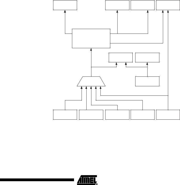
Figure 18 presents the principal clock systems in the AVR and their distribution. All of the clocks need not be active at a given time. In order to reduce power consumption, the clocks to modules not being used can be halted by using different sleep modes, as described in “Power Management and Sleep Modes” on page 40. The clock systems are detailed below.
Figure 18. Clock Distribution |
|
|
|
||
General I/O |
|
CPU Core |
RAM |
Flash and |
|
Modules |
|
EEPROM |
|||
|
|
|
|||
clkI/O |
AVR Clock |
clkCPU |
|
|
|
|
Control Unit |
|
|
|
|
|
|
clkFLASH |
|
|
|
|
|
Reset Logic |
Watchdog Timer |
|
|
|
Source clock |
Watchdog clock |
|
||
|
Clock |
|
Watchdog |
|
|
|
Multiplexer |
|
Oscillator |
|
|
External RC |
External Clock |
Crystal |
Low-frequency |
Calibrated RC |
|
Oscillator |
Oscillator |
Crystal Oscillator |
Oscillator |
||
|
CPU Clock – clkCPU |
The CPU clock is routed to parts of the system concerned with operation of the AVR |
|
core. Examples of such modules are the General Purpose Register File, the Status Reg- |
|
ister, and the Data memory holding the Stack Pointer. Halting the CPU clock inhibits the |
|
core from performing general operations and calculations. |
I/O Clock – clkI/O |
The I/O clock is used by the majority of the I/O modules, like Timer/Counters, SPI, and |
|
USART. The I/O clock is also used by the External Interrupt module, but note that some |
|
external interrupts are detected by asynchronous logic, allowing such interrupts to be |
|
detected even if the I/O clock is halted. |
33
2512G–AVR–03/05