

- •Release History
- •Contents
- •List of Figures
- •List of Tables
- •1 TMS320TCI6618 Features
- •1.1 KeyStone Architecture
- •1.2 Device Description
- •1.3 Functional Block Diagram
- •2 Device Overview
- •2.1 Device Characteristics
- •2.2 CPU (DSP Core) Description
- •2.3 Memory Map Summary
- •2.4 Boot Sequence
- •2.5 Boot Modes Supported and PLL Settings
- •2.5.1 Boot Device Field
- •2.5.2 Device Configuration Field
- •2.5.2.1 No Boot Device Configuration
- •2.5.2.2 Serial Rapid I/O Boot Device Configuration
- •2.5.2.3 Ethernet (SGMII) Boot Device Configuration
- •2.5.2.4 PCI Boot Device Configuration
- •2.5.2.5 I2C Boot Device Configuration
- •2.5.2.6 SPI Boot Device Configuration
- •2.5.2.7 HyperLink Boot Device Configuration
- •2.5.3 PLL Settings
- •2.6 Second-Level Bootloaders
- •2.7 Terminals
- •2.8 Terminal Functions
- •2.9 Development
- •2.9.1 Development Support
- •2.9.2 Device Support
- •Related Documentation from Texas Instruments
- •3 Device Configuration
- •3.1 Device Configuration at Device Reset
- •3.2 Peripheral Selection After Device Reset
- •3.3 Device State Control Registers
- •3.3.1 Device Status (DEVSTAT) Register
- •3.3.2 Device Configuration Register
- •3.3.3 JTAG ID (JTAGID) Register Description
- •3.3.4 Kicker Mechanism (KICK0 and KICK1) Register
- •3.3.5 LRESETNMI PIN Status (LRSTNMIPINSTAT) Register
- •3.3.6 LRESETNMI PIN Status Clear (LRSTNMIPINSTAT_CLR) Register
- •3.3.7 Reset Status (RESET_STAT) Register
- •3.3.8 Reset Status Clear (RESET_STAT_CLR) Register
- •3.3.9 Boot Complete (BOOTCOMPLETE) Register
- •3.3.10 Power State Control (PWRSTATECTL) Register
- •3.3.11 NMI Even Generation to CorePac (NMIGRx) Register
- •3.3.12 IPC Generation (IPCGRx) Registers
- •3.3.13 IPC Acknowledgement (IPCARx) Registers
- •3.3.14 IPC Generation Host (IPCGRH) Register
- •3.3.15 IPC Acknowledgement Host (IPCARH) Register
- •3.3.16 Timer Input Selection Register (TINPSEL)
- •3.3.17 Timer Output Selection Register (TOUTPSEL)
- •3.3.18 Reset Mux (RSTMUXx) Register
- •3.4 Pullup/Pulldown Resistors
- •4 System Interconnect
- •4.1 Internal Buses, Bridges, and Switch Fabrics
- •4.2 Data Switch Fabric Connections
- •4.3 Configuration Switch Fabric
- •4.4 Bus Priorities
- •5 C66x CorePac
- •5.1 Memory Architecture
- •5.1.1 L1P Memory
- •5.1.2 L1D Memory
- •5.1.3 L2 Memory
- •5.1.4 MSM SRAM
- •5.1.5 L3 Memory
- •5.2 Memory Protection
- •5.3 Bandwidth Management
- •5.4 Power-Down Control
- •5.5 CorePac Resets
- •5.6 CorePac Revision
- •5.7 C66x CorePac Register Descriptions
- •6 Device Operating Conditions
- •6.1 Absolute Maximum Ratings
- •6.2 Recommended Operating Conditions
- •6.3 Electrical Characteristics
- •7 TMS320TCI6618 Peripheral Information and Electrical Specifications
- •7.1 Parameter Information
- •7.1.1 1.8-V Signal Transition Levels
- •7.1.2 Timing Parameters and Board Routing Analysis
- •7.2 Recommended Clock and Control Signal Transition Behavior
- •7.3 Power Supplies
- •7.3.1 Power-Up Sequencing
- •7.3.1.1 Core-Before-IO Power Sequencing
- •7.3.1.2 IO-Before-Core Power Sequencing
- •7.3.1.3 Prolonged Resets
- •7.3.2 Power-Down Sequence
- •7.3.3 Power Supply Decoupling and Bulk Capacitors
- •7.3.4 SmartReflex
- •7.4 Enhanced Direct Memory Access (EDMA3) Controller
- •7.4.1 EDMA3 Device-Specific Information
- •7.4.2 EDMA3 Channel Synchronization Events
- •7.5 Interrupts
- •7.5.1 Interrupt Sources and Interrupt Controller
- •7.5.2 INTC Registers
- •7.5.2.1 INTC0 Register Map
- •7.5.2.2 INTC1 Register Map
- •7.5.2.3 INTC2 Register Map
- •7.5.3 Inter-Processor Register Map
- •7.5.4 NMI and LRESET
- •7.5.5 External Interrupts Electrical Data/Timing
- •7.6 Memory Protection Unit (MPU)
- •7.6.1 MPU Registers
- •7.6.1.1 MPU Register Map
- •7.6.1.2 Device-Specific MPU Registers
- •7.6.2 MPU Programmable Range Registers
- •7.6.2.1 Programmable Range n Start Address Register (PROGn_MPSAR)
- •7.6.2.2 Programmable Range n - End Address Register (PROGn_MPEAR)
- •7.6.2.3 Programmable Range n Memory Protection Page Attribute Register (PROGn_MPPA)
- •7.7 Reset Controller
- •7.7.1 Power-on Reset
- •7.7.2 Hard Reset
- •7.7.3 Soft Reset
- •7.7.4 Local Reset
- •7.7.5 Reset Priority
- •7.7.6 Reset Controller Register
- •7.7.7 Reset Electrical Data/Timing
- •7.8 Main PLL and the PLL Controller
- •7.8.1 Main PLL Controller Device-Specific Information
- •7.8.1.1 Internal Clocks and Maximum Operating Frequencies
- •7.8.1.2 Main PLL Controller Operating Modes
- •7.8.1.3 Main PLL Stabilization, Lock, and Reset Times
- •7.8.2 PLL Controller Memory Map
- •7.8.2.1 PLL Secondary Control Register (SECCTL)
- •7.8.2.2 PLL Controller Divider Register (PLLDIV2, PLLDIV5, PLLDIV8)
- •7.8.2.3 PLL Controller Clock Align Control Register (ALNCTL)
- •7.8.2.4 PLLDIV Divider Ratio Change Status Register (DCHANGE)
- •7.8.2.5 SYSCLK Status Register (SYSTAT)
- •7.8.2.6 Reset Type Status Register (RSTYPE)
- •7.8.2.7 Reset Control Register (RSTCTRL)
- •7.8.2.8 Reset Configuration Register (RSTCFG)
- •7.8.2.9 Reset Isolation Register (RSISO)
- •7.8.3 Main PLL Control Registers
- •7.8.4 Main PLL Controller/SRIO/HyperLink/PCIe Clock Input Electrical Data/Timing
- •7.9.1 DDR3 PLL Control Register
- •7.9.2 DDR3 PLL Device-Specific Information
- •7.9.3 DDR3 PLL Input Clock Electrical Data/Timing
- •7.10 PASS PLL
- •7.10.1 PASS PLL Control Register
- •7.10.2 PASS PLL Device-Specific Information
- •7.10.3 PASS PLL Input Clock Electrical Data/Timing
- •7.11 DDR3 Memory Controller
- •7.11.1 DDR3 Memory Controller Device-Specific Information
- •7.11.2 DDR3 Memory Controller Electrical Data/Timing
- •7.12 I2C Peripheral
- •7.12.1 I2C Device-Specific Information
- •7.12.2 I2C Peripheral Register Description(s)
- •7.12.3 I2C Electrical Data/Timing
- •7.12.3.1 Inter-Integrated Circuits (I2C) Timing
- •7.13 SPI Peripheral
- •7.13.1 SPI Electrical Data/Timing
- •7.13.1.1 SPI Timing
- •7.14 HyperLink Peripheral
- •7.15 UART Peripheral
- •7.16 PCIe Peripheral
- •7.17 Packet Accelerator
- •7.18 Security Accelerator
- •7.19 Ethernet MAC (EMAC)
- •7.20 Management Data Input/Output (MDIO)
- •7.21 Timers
- •7.21.1 Timers Device-Specific Information
- •7.21.2 Timers Electrical Data/Timing
- •7.22 Rake Search Accelerator (RSA)
- •7.23 Enhanced Viterbi-Decoder Coprocessor (VCP2)
- •7.24 Third-Generation Turbo Decoder Coprocessor (TCP3d)
- •7.25 Turbo Encoder Coprocessor (TCP3e)
- •7.26 Bit Rate Coprocessor (BCP)
- •7.27 Serial RapidIO (SRIO) Port
- •7.28 General-Purpose Input/Output (GPIO)
- •7.28.1 GPIO Device-Specific Information
- •7.28.2 GPIO Electrical Data/Timing
- •7.29 Semaphore2
- •7.30 Antenna Interface Subsystem 2
- •7.33 FFTC
- •7.34 Emulation Features and Capability
- •7.34.1 Advanced Event Triggering (AET)
- •7.34.2 Trace
- •7.34.2.1 Trace Electrical Data/Timing
- •7.34.3 IEEE 1149.1 JTAG
- •7.34.3.1 IEEE 1149.1 JTAG Compatibility Statement
- •7.34.3.2 JTAG Electrical Data/Timing
- •8 Mechanical Data
- •8.1 Packaging Information
- •8.2 Package CYP
INFORMATION ADVANCE
TMS320TCI6618
Communications Infrastructure KeyStone SoC
SPRS688—February 2011 |
www.ti.com |
|
7.34.2 Trace
The TCI6618 device supports trace. Trace is a debug technology that provides a detailed, historical account of application code execution, timing, and data accesses. Trace collects, compresses, and exports debug information for analysis. Trace works in real-time and does not impact the execution of the system.
For more information on board design guidelines for trace advanced emulation, see the Emulation and Trace Headers Technical Reference in ‘‘Related Documentation from Texas Instruments’’ on page 59.
7.34.2.1 Trace Electrical Data/Timing
Table 7-84 |
Trace Switching Characteristics (1) |
|
|
|
||
(see Figure 7-60) |
|
|
|
|
|
|
|
|
|
|
|
|
|
No. |
|
|
Parameter |
Min |
Max |
Unit |
1 |
tw(DPnH) |
|
Pulse duration, DPn/EMUn high |
2.4 |
|
ns |
1 |
tw(DPnH)90% |
Pulse duration, DPn/EMUn high detected at 90% Voh |
1.5 |
|
ns |
|
2 |
tw(DPnL) |
|
Pulse duration, DPn/EMUn low |
2.4 |
|
ns |
2 |
tw(DPnL)10% |
Pulse duration, DPn/EMUn low detected at 10% Voh |
1.5 |
|
ns |
|
3 |
tsko(DPn) |
|
Output skew time, time delay difference between DPn/EMUn pins configured as trace |
-500 |
500 |
ps |
|
tskp(DPn) |
|
Pulse skew, magnitude of difference between high-to-low (tphl) and low-to-high (tplh) propagation delays. |
|
600 |
ps |
|
tσλδπ_ο(DPn) |
Output slew rate DPn/EMUn |
3.3 |
|
V/ns |
|
End of Table 7-84 |
|
|
|
|
||
|
|
|
|
|
||
1 Over recommended operating conditions. |
|
|
|
|||
Figure 7-60 |
Trace Timing |
|
|
|
|
|
|
|
|
|
|
|
||||||||||||
|
|
|
|
|
|
|
|
|
|
|
|
|
|
|
|
|
|
|||||||
|
A |
|
|
|
|
|
|
|
|
|
|
|
||||||||||||
|
|
|
|
|
|
|
|
|
|
|
|
|
|
|
|
|
|
|
|
|
|
|
||
|
|
TPLH |
|
|
|
|
|
|
|
|
|
|
|
|
|
TPHL |
|
|
|
|
|
|
|
|
|
|
|
|
|
|
|
|
|
|
|
|
|
|
|||||||||||
|
1 |
|
|
|
2 |
|
|
|
|
|
|
|
||||||||||||
|
|
|
|
|
|
|
|
|
|
|
|
|
|
|
|
|
|
|
|
|
|
|
|
|
B
3
C
7.34.3 IEEE 1149.1 JTAG
The JTAG interface is used to support boundary scan and emulation of the device. The boundary scan supported allows for an asynchronous TRST and only the 5 baseline JTAG signals (e.g., no EMU[1:0]) required for boundary scan. Most interfaces on the device follow the Boundary Scan Test Specification (IEEE1149.1), while all of the SerDes (SRIO and SGMII) support the AC-coupled net test defined in AC-Coupled Net Test Specification (IEEE1149.6).
It is expected that all compliant devices are connected through the same JTAG interface, in daisy-chain fashion, in accordance with the specification. The JTAG interface uses 1.8-V LVCMOS buffers, compliant with the Power Supply Voltage and Interface Standard for Nonterminated Digital Integrated Circuit Specification (EAI/JESD8-5).
194 |
Copyright 2011 Texas Instruments Incorporated |

TMS320TCI6618
Communications Infrastructure KeyStone SoC
www.ti.com |
SPRS688—February 2011 |
|
7.34.3.1 IEEE 1149.1 JTAG Compatibility Statement
For maximum reliability, the TCI6618 DSP includes an internal pulldown (IPD) on the TRST pin to ensure that TRST will always be asserted upon power up and the DSP's internal emulation logic will always be properly initialized when this pin is not routed out. JTAG controllers from Texas Instruments actively drive TRST high. However, some third-party JTAG controllers may not drive TRST high but expect the use of an external pullup resistor on TRST. When using this type of JTAG controller, assert TRST to initialize the DSP after powerup and externally drive TRST high before attempting any emulation or boundary scan operations.
7.34.3.2 JTAG Electrical Data/Timing
Table 7-85 JTAG Test Port Timing Requirements
(see Figure 7-61)
No. |
|
|
Min |
Max |
Unit |
1 |
tc(TCK) |
Cycle time, TCK |
20 |
|
ns |
1a |
tw(TCKH) |
Pulse duration, TCK high (40% of tc) |
8 |
|
ns |
|
|
|
|
|
|
1b |
tw(TCKL) |
Pulse duration, TCK low(40% of tc) |
8 |
|
ns |
|
|
|
|
|
|
3 |
tsu(TDI-TCK) |
input setup time, TDI valid to TCK high |
2 |
|
ns |
|
|
|
|
|
|
3 |
tsu(TMS-TCK) |
input setup time, TMS valid to TCK high |
2 |
|
ns |
|
|
|
|
|
|
4 |
th(TCK-TDI) |
input hold time, TDI valid from TCK high |
10 |
|
ns |
|
|
|
|
|
|
4 |
th(TCK-TMS) |
input hold time, TMS valid from TCK high |
10 |
|
ns |
|
|
|
|
|
|
End of Table 7-85 |
|
|
|
|
|
|
|
|
|
|
|
Table 7-86 |
JTAG Test Port Switching Characteristics (1) |
|
|
|
||
(see Figure 7-61) |
|
|
|
|
|
|
|
|
|
|
|
|
|
No. |
|
|
Parameter |
Min |
Max |
Unit |
2 |
td(TCKL-TDOV) |
Delay time, TCK low to TDO valid |
|
8 |
ns |
|
End of Table 7-86 |
|
|
|
|
||
|
|
|
|
|
||
1 Over recommended operating conditions. |
|
|
|
|||
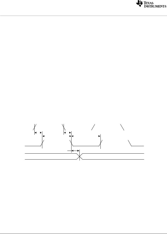
Figure 7-61 JTAG Test-Port Timing
1
1a |
1b |
|
|
TCK
2
TDO
4
3
TDI / TMS
ADVANCE INFORMATION
Copyright 2011 Texas Instruments Incorporated |
195 |