

TMS320TCI6618
Communications Infrastructure KeyStone SoC
www.ti.com |
SPRS688—February 2011 |
|
1 TMS320TCI6618 Features
•Four TMS320C66x™ DSP Core Subsystems, Each With
–1.2 GHz C66x Fixed/Floating-Point DSP Core
›32 GMacs/Core for Fixed Point @ 1.2 GHz
›16 GFlops/Core for Floating Point @ 1.2 GHz
–Memory
›32K Byte L1P Per Core
›32K Byte L1D Per Core
›1024K Byte Local L2 Per Core
•Multicore Shared Memory Controller (MSMC)
–2048 KB MSM SRAM Memory Shared by Four DSP Cores
–Memory Protection Unit for Both MSM SRAM and DDR3_EMIF
•Hardware Coprocessors
–Three Enhanced Coprocessors for Turbo Decoding
›Supports WCDMA/HSPA/HSPA+/TD-SCDMA, LTE, and WiMAX
›Supports up to 548 Mbps for LTE and up to 353 Mbps
for WCDMA
›Low DSP Overhead – HW Interleaver Table Generation and CRC Check
–One Enhanced Coprocessor for Turbo Encoding
›Supports up to 643 Mbps for LTE and up to 746 Mbps for WCDMA
–Four Viterbi Decoders
›Supports More Than 38 Mbps @ 40 bit Block Size
–Two WCDMA Receive Acceleration Coprocessors
›Up to 256 Users @ 8 Fingers w/o Measurement
–WCDMA Transmit Acceleration Coprocessor
›Up to 256 Users with two Radio Links and Diversity
–Three Fast Fourier Transform Coprocessors
›2048 pt FFT in 4.8 μs
–Bit Rate Coprocessor
›WCDMA/HSPA+, TD-SCDMA, LTE, and WiMAX Uplink and Downlink Bit Processing
›Includes Encoding, Rate Matching/Dematching, Segmentation, Multiplexing, and More
›Supports Up To 914 Mbps for LTE and 405 Mbps for WCDMA/TD-SCDMA
•Multicore Navigator
–8192 Multipurpose Hardware Queues with Queue Manager
–Packet-Based DMA for Zero-Overhead Transfers
•Network Coprocessors
–Packet Accelerator Enables Support for
›Transport Plane IPsec, GTP-U, SCTP, PDCP
›L2 User Plane PDCP (RoHC, Air Ciphering)
›1 Gbps Wire Speed Throughput at 1.5M Packets Per Second
–Security Accelerator Engine Enables Support for
›IPSec, SRTP, 3GPP and WiMAX Air Interface, and SSL/TLS Security
›ECB, CBC, CTR, F8, A5/3, CCM, GCM, HMAC, CMAC, GMAC, AES, DES, 3DES, Kasumi, SNOW 3G, SHA-1, SHA-2 (256-bit Hash), MD5
›Up to 2.8 Gbps Encryption Speed
•Four Rake/Search Accelerators (RSA) for
–Chip Rate Processing for WCDMA Rel'99, HSDPA, and HSDPA+
–Reed-Muller Decoding
•Peripherals
–Six Lane SerDes-Based Antenna Interface (AIF2)
›Operating at up to 6.144 Gbps
›Compliant with OBSAI RP3 and CPRI Standards for 3G / 4G (WCDMA, LTE TDD, LTE FDD, TD-SCDMA, and WiMAX)
–Four Lanes of SRIO 2.1
›5 GBaud Operation Per Lane
›Supports Direct I/O, Message Passing
–Two Lanes PCIe Gen2
›Supports Up To 5 GBaud
–Hyperlink
›Supports Connections to Other KeyStone Architecture Devices Providing Resource Scalability
›Supports up to 50 Gbaud
–Ethernet MAC Subsystem (EMAC)
›Two SGMII Ports
›IEEE1588 Support
–64-Bit DDR3 Interface with Speeds up to 1333 MHz
–UART Interface
–I2C Interface
–16 GPIO pins
–SPI Interface
–Semaphore Module
–Eight 64-Bit Timers
–Three On-Chip PLLs
•Commercial Temperature:
–0°C to 100°C
•Extended Temperature:
–- 40°C to 100°C
ADVANCE INFORMATION
Copyright 2011 Texas Instruments Incorporated

INFORMATION ADVANCE
TMS320TCI6618
Communications Infrastructure KeyStone SoC
SPRS688—February 2011 |
www.ti.com |
|
1.1 KeyStone Architecture
TI’s KeyStone Multicore Architecture provides a high performance structure for integrating RISC and DSP cores with application specific coprocessors and I/O. KeyStone is the first of its kind that provides adequate internal bandwidth for nonblocking access to all processing cores, peripherals, coprocessors, and I/O. This is achieved with four main hardware elements: Multicore Navigator, TeraNet, Multicore Shared Memory Controller, and HyperLink.
Multicore Navigator is an innovative packet-based manager that controls 8192 queues. When tasks are allocated to the queues, Multicore Navigator provides hardware-accelerated dispatch that directs tasks to the appropriate available hardware. The packet-based system on a chip (SoC) uses the two Tbps capacity of the TeraNet switched central resource to move packets. The Multicore Shared Memory Controller enables processing cores to access shared memory directly without drawing from TeraNet’s capacity, so packet movement cannot be blocked by memory access.
HyperLink provides a 50-Gbps chip-level interconnect that allows SoCs to work in tandem. Its low-protocol overhead and high throughput make Hyperlink an ideal interface for chip-to-chip interconnections. Working with Multicore Navigator, HyperLink dispatches tasks to tandem devices transparently and executes tasks as if they are running on local resources.
1.2 Device Description
The TMS320TCI6618 Communications Infrastructure KeyStone SoC is a member of the C66xx SoC family based on TI's new KeyStone Multicore SoC Architecture designed specifically for high performance wireless infrastructure applications. The TCI6618 provides a very high performance macro basestation platform for developing all wireless standards including WCDMA/HSPA/HSPA+, TD-SCDMA, GSM, TDD-LTE, FDD-LTE, and WiMAX. Even with aggregate data rates for 20-MHz LTE systems above 400 Mbps per sector, the TCI6618 can support two sectors running at full rate. The TCI6618 also sets a new standard for clock speed with operating frequencies up to 1.2 GHz.
TI's SoC architecture provides a programmable platform integrating various subsystems (C66x cores, IP network, radio layers 1 and 2, and transport processing) and uses a queue-based communication system that allows the SoC resources to operate efficiently and seamlessly. This unique SoC architecture also includes a TeraNet Switch that enables the wide mix of system elements, from programmable cores to dedicated coprocessors and high speed IO, to each operate at maximum efficiency with no blocking or stalling.
TI's new C66x core launches a new era of DSP technology by combining fixed point and floating point computational capability in the processor without sacrificing speed, size, or power consumption. The
raw computational performance is an industry-leading 32 GMACS/core and 16 Gflops/core (@ 1.2 GHz operating frequency). The C66x is also 100% backward compatible with software for C64x+ devices. The C66x core incorporates 90 new instructions targeted for floating point (FPi) and vector math oriented (VPi) processing. These enhancements yield tremendous performance improvements in multi-antenna 4.8G signal processing for algorithms like MIMO and beamforming.
The TCI6618 contains many wireless basestation coprocessors to offload the bulk of the processing demands of layer 1 and layer 2 base station processing. This keeps the cores free for receiver algorithms and other differentiating functions. The SoC contains numerous copies of key coprocessors such as the FFTC and TCP3d. A key coprocessor for enabling high data rates is the bit rate coprocessor (BCP), which handles the entire downlink bit processing chain and much of the receive bit processing. The architectural elements of the SoC (Multicore Navigator) ensure that all the bits are processed without any CPU intervention or overhead, allowing the system to make optimal use of its resources.
12 |
Copyright 2011 Texas Instruments Incorporated |
TMS320TCI6618
Communications Infrastructure KeyStone SoC
www.ti.com |
SPRS688—February 2011 |
|
TI's scalable multicore SoC architecture solutions provide developers with a range of softwareand hardware-compatible devices to minimize development time and maximize reuse across all base station platforms from Femto to Macro.
The TCI6618 device has a complete set of development tools that includes: a C compiler, an assembly optimizer to simplify programming and scheduling, and a Windows debugger interface for visibility into source code execution.
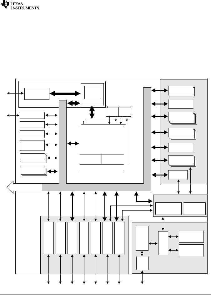
1.3 Functional Block Diagram
Figure 1-1 shows the functional block diagram of the TMS320TCI6618 device.
Figure 1-1 Functional Block Diagram
Memory Subsystem |
|
|
|
|
|
Coprocessors |
INFORMATION |
||||
|
|
|
|
|
|
|
|
||||
64-Bit |
|
|
|
2MB |
|
|
|
RAC |
2 |
||
|
|
|
MSM |
|
|
|
|||||
|
|
|
|
|
|
|
|
||||
DDR3 EMIF |
|
|
|
SRAM |
|
|
|
|
|
|
|
|
|
|
|
MSMC |
|
|
|
TAC |
|
||
|
|
|
|
|
|
|
|
|
|||
Debug & Trace |
|
|
|
|
RSA |
RSA |
|
|
|
|
|
|
|
|
|
|
|
2 |
VCP2 |
|
|||
|
|
|
|
|
|
|
4 |
||||
|
|
|
|
|
|
|
|
|
|||
|
|
|
|
|
|
|
|
|
|
||
Boot ROM |
|
|
|
|
|
|
|
|
|
|
|
|
|
|
|
|
|
|
|
TCP3d |
|
||
Semaphore |
|
|
|
C66x™ |
|
|
3 |
ADVANCE |
|||
|
|
|
|
|
|
|
|||||
|
|
|
|
|
|
|
|
|
|||
Power |
|
|
|
CorePac |
|
|
|
|
|
||
Management |
|
|
|
|
|
|
|
TCP3e |
|
||
PLL |
|
|
32KB L1 |
32KB L1 |
|
FFTC |
|
||||
|
|
|
|
|
|||||||
|
|
|
P-Cache |
D-Cache |
|
3 |
|||||
3 |
|
|
|
|
|
||||||
|
|
|
1024KB L2 Cache |
|
|
|
|
|
|||
EDMA |
|
|
|
|
|
|
|
|
|||
|
|
|
|
|
|
|
|
|
|
||
3 |
|
|
4 Cores @ 1.0 GHz / 1.2 GHz |
|
BCP |
|
|
||||
|
|
|
|
|
|
|
|||||
HyperLink |
|
|
|
TeraNet |
|
|
|
|
|
|
|
|
|
|
|
|
|
|
|
Multicore Navigator |
|
||
|
|
|
|
|
|
|
|
Queue |
Packet |
|
|
|
|
|
|
|
|
|
|
Manager |
|
DMA |
|
Others |
C |
PCIe 2 |
UART |
SPI |
AIF2 6 |
SRIO 4 |
Ethernet Switch |
Switch |
Security |
|
|
Accelerator |
|
||||||||||
2 |
|
||||||||||
I |
Packet |
|
|||||||||
|
|
|
|
|
|
|
|
|
Accelerator |
|
|
|
|
|
|
|
|
|
SGMII2 |
Network Coprocessor |
|
||
TCI6618 |
|
|
|
|
|
|
|
|
|||
|
|
|
|
|
|
|
|
|
|
|
|
Copyright 2011 Texas Instruments Incorporated |
13 |