

TMS320C6203B FIXED POINT DIGITAL SIGNAL PROCESSOR
SPRS086K – JANUARY 1999 – REVISED APRIL 2003
DHigh-Performance Fixed-Point Digital Signal Processor (DSP) – TMS320C62x
–4-, 3.33-ns Instruction Cycle Time
–250-, 300-MHz Clock Rate
–Eight 32-Bit Instructions/Cycle
–2000, 2400 MIPS
DC6203B and C6202 GLS Ball Grid Array
(BGA) Packages are Pin-Compatible With the C6204 GLW BGA Package†
DC6203B and C6202B GNZ and GNY Packages are Pin-Compatible
DVelociTI Advanced Very-Long-Instruction- Word (VLIW) C62x DSP Core
–Eight Highly Independent Functional Units:
–Six ALUs (32-/40-Bit)
–Two 16-Bit Multipliers (32-Bit Result)
–Load-Store Architecture With 32 32-Bit General-Purpose Registers
–Instruction Packing Reduces Code Size
–All Instructions Conditional
DInstruction Set Features
–Byte-Addressable (8-, 16-, 32-Bit Data)
–8-Bit Overflow Protection
–Saturation
–Bit-Field Extract, Set, Clear
–Bit-Counting
–Normalization
D7M-Bit On-Chip SRAM
–3M-Bit Internal Program/Cache
(96K 32-Bit Instructions)
–4M-Bit Dual-Access Internal Data
(512K Bytes)
–Organized as Two 256K-Byte Blocks for Improved Concurrency
D32-Bit External Memory Interface (EMIF)
–Glueless Interface to Synchronous Memories: SDRAM or SBSRAM
–Glueless Interface to Asynchronous Memories: SRAM and EPROM
–52M-Byte Addressable External Memory Space
DFour-Channel Bootloading Direct-Memory-Access (DMA) Controller With an Auxiliary Channel
DFlexible Phase-Locked-Loop (PLL) Clock Generator
D32-Bit Expansion Bus (XBus)
–Glueless/Low-Glue Interface to Popular PCI Bridge Chips
–Glueless/Low-Glue Interface to Popular Synchronous or Asynchronous Microprocessor Buses
–Master/Slave Functionality
–Glueless Interface to Synchronous FIFOs and Asynchronous Peripherals
DThree Multichannel Buffered Serial Ports (McBSPs)
–Direct Interface to T1/E1, MVIP, SCSA Framers
–ST-Bus-Switching Compatible
–Up to 256 Channels Each
–AC97-Compatible
–Serial-Peripheral Interface (SPI) Compatible (Motorola )
DTwo 32-Bit General-Purpose Timers
DIEEE-1149.1 (JTAG‡) Boundary-Scan-Compatible
D352-Pin BGA Package (GNZ)
D384-Pin BGA Package (GLS)
D384-Pin BGA Package (GNY)
D0.15- m/5-Level Metal Process
–CMOS Technology
D3.3-V I/Os, 1.5-V Internal
Please be aware that an important notice concerning availability, standard warranty, and use in critical applications of Texas Instruments semiconductor products and disclaimers thereto appears at the end of this data sheet.
TMS320C62x, VelociTI, and C62x are trademarks of Texas Instruments. |
|
|
|
Motorola is a trademark of Motorola, Inc. |
|
|
|
All trademarks are the property of their respective owners. |
|
|
|
† |
For more details, see the GLS BGA package bottom view. |
|
|
‡ |
IEEE Standard 1149.1-1990 Standard-Test-Access Port and Boundary Scan Architecture. |
|
|
|
|
|
|
PRODUCTION DATA information is current as of publication date. |
Copyright 2003, Texas Instruments Incorporated |
||
Products conform to specifications per the terms of Texas Instruments |
|
|
|
standard warranty. Production processing does not necessarily include |
|
|
|
testing of all parameters. |
|
|
|
|
POST OFFICE BOX 1443 • HOUSTON, TEXAS 77251–1443 |
1 |
|
TMS320C6203B
FIXED POINT DIGITAL SIGNAL PROCESSOR
SPRS086K – JANUARY 1999 – REVISED APRIL 2003
|
Table of Contents |
|
|||||
revision history . . . . . . . . . . . . . . . . . . . . . . . . . . . . . . . . . . |
. . 2 |
parameter measurement information . . . . . . . . . . . . . . . |
44 |
||||
GNZ, GLS, and GNY BGA packages (bottom view) . . . . 4 |
signal transition levels . . . . . . . . . . . . . . . . . . . . . . . . . . |
44 |
|||||
description . . . . . . . . . . . . . . . . . . . . . . . . . . . . . . . . . . . . . |
. . 6 |
timing parameters and board routing analysis . . . . . . |
45 |
||||
device characteristics . . . . . . . . . . . . . . . . . . . . . . . . . . . . |
. . 6 |
input and output clocks |
46 |
||||
C62x device compatibility |
8 |
||||||
asynchronous memory timing |
49 |
||||||
functional and CPU (DSP core) block diagram |
9 |
||||||
synchronous-burst memory timing |
52 |
||||||
CPU (DSP core) description |
10 |
||||||
synchronous DRAM timing |
56 |
||||||
memory map summary . . . . . . . . . . . . . . . . . . . . . . . . . . . . |
12 |
||||||
peripheral register descriptions |
13 |
|
|
|
|
63 |
|
HOLD/HOLDA timing . . . . . . . . . . . . . . . . . . . . . . . . . . . . |
|||||||
DMA synchronization events . . . . . . . . . . . . . . . . . . . . . . . |
18 |
reset timing . . . . . . . . . . . . . . . . . . . . . . . . . . . . . . . . . . . . . |
64 |
||||
interrupt sources and interrupt selector . . . . . . . . . . . . . . |
19 |
external interrupt timing |
66 |
||||
signal groups description |
20 |
||||||
expansion bus synchronous FIFO timing |
67 |
||||||
signal descriptions |
23 |
||||||
expansion bus asynchronous peripheral timing |
69 |
||||||
development support |
34 |
||||||
expansion bus synchronous host-port timing |
72 |
||||||
documentation support |
37 |
||||||
|
|
|
|
|
|||
clock PLL . . . . . . . . . . . . . . . . . . . . . . . . . . . . . . . . . . . . . . . |
38 |
expansion bus asynchronous host-port timing . . . . . . . |
78 |
||||
power-supply sequencing . . . . . . . . . . . . . . . . . . . . . . . . . . |
41 |
XHOLD/XHOLDA timing . . . . . . . . . . . . . . . . . . . . . . . . . . |
80 |
||||
IEEE 1149.1 JTAG compatibility statement . . . . . . . . . . . |
42 |
multichannel buffered serial port timing |
82 |
||||
absolute maximum ratings over operating case |
|
||||||
|
DMAC, timer, power-down timing |
94 |
|||||
temperature ranges |
43 |
||||||
JTAG test-port timing |
96 |
||||||
recommended operating conditions . . . . . . . . . . . . . . . . . |
43 |
||||||
electrical characteristics over recommended ranges |
|
mechanical data . . . . . . . . . . . . . . . . . . . . . . . . . . . . . . . . . |
97 |
||||
of supply voltage and operating case temperature . . |
43 |
|
|
|
|
|
|
|
|
|
|
|
|
|
|
REVISION HISTORY
This data sheet revision history highlights the technical changes made to the SPRS086J device-specific data sheet to make it an SPRS086K revision.
SCOPE: Applicable updates to the C62x device family, specifically to the C6203B devices, have been incorporated. Added device-specific information for the new extended-temperature device (C6203BGNZA-250). Deleted C6203BGNZA-300 device reference.
PAGE(S)
ADDITIONS/CHANGES/DELETIONS
NO.
7Table 1, Characteristics of the Pin-Compatible DSPs:
Added extended-temperature device-specific information for C6203B and C6202B device columns.
Changed the device product status for the C6202B device from Advance Information (AI) to Production Data (PD) Deleted footnote description of PRODUCT PREVIEW and ADVANCE INFORMATION
8C62x Device Compatibility section:
Added “device clock speeds” bullet and paragraph explanation
36Table 15, TMS320C6203B Device Part Numbers (P/Ns) and Ordering Information:
Deleted extended-temperature device – TMS320C6203BGNZA-173, 300 MHz/2400 MIPS, 1.7 V, 3.3 V, –40° C to 105° C Corrected the device orderable P/N from “TMS32C6203BGNZA173” to “TMS32C6203BGNZA250” [May 2003].
36Figure 4, TMS320C6000 DSP Platform Device Nomenclature (Including TMS320C6203B): Added additional devices to the “C6000 DSP:” category
37Documentation Support section:
Added paragraph referencing the TMS320C6203, TMS320C6203B Digital Signal Processors Silicon Errata
[literature number SPRZ174]
Added paragraph referencing the Using IBIS Models for Timing Analysis application report [literature number SPRA839]
2 |
POST OFFICE BOX 1443 • HOUSTON, TEXAS 77251–1443 |

TMS320C6203B
FIXED POINT DIGITAL SIGNAL PROCESSOR
SPRS086K – JANUARY 1999 – REVISED APRIL 2003
PAGE(S) |
ADDITIONS/CHANGES/DELETIONS |
|
NO. |
||
|
38Clock PLL section:
Deleted Table 16, Compatible CLKIN External Clock Source and associated paragraph reference
43–96 Electricals:
Added the device-specific information on the extended-temperature device (C6203BGNZA-250)
43Absolute Maximum Ratings Over Operating Case Temperature Ranges section:
Added the extended-temperature device-specific information to the “Operating case temperature ranges, TC: (A version)”
43Recommended Operating Conditions table: Added “:C6203BGNZA-250” to the A version of TC
45Timing Parameters and Board Routing Analysis section:
Added reference to the Using IBIS Models for Timing Analysis application report (literature number SPRA839) in first paragraph.
Changed the title of Table 19 to “Board-Level Timings Example” Changed the title of Figure 11 to “Board-Level Input/Output Timings”
53Synchronous-Burst Memory Timing section:
Timing Requirements for Synchronous-Burst SRAM Cycles for C6203B Rev. 3 table: Added C6203BGNZA-250 extended-temperature device
Deleted C6203BGNZA173-300 extended-temperature device
53–54 Synchronous-Burst Memory Timing section:
Switching Characteristics Over Recommended Operating Conditions for Synchronous-Burst SRAM Cycles for C6203B Rev. 3 table:
Added C6203BGNZA-250 extended-temperature device Deleted C6203BGNZA173-300 extended-temperature device
57Synchronous DRAM Timing section:
Timing Requirements for Synchronous DRAM Cycles for C6203B Rev. 3 table: Added C6203BGNZA-250 extended-temperature device
Deleted C6203BGNZA173-300 extended-temperature device
58–59 Synchronous DRAM Timing section:
Switching Characteristics Over Recommended Operating Conditions for Synchronous DRAM Cycles for C6203B Rev. 3 table:
Added C6203BGNZA-250 extended-temperature device Deleted C6203BGNZA173-300 extended-temperature device
97 Replaced GNZ (S-PBGA-N352) mechanical with latest version
POST OFFICE BOX 1443 • HOUSTON, TEXAS 77251–1443 |
3 |
TMS320C6203B
FIXED POINT DIGITAL SIGNAL PROCESSOR
SPRS086K – JANUARY 1999 – REVISED APRIL 2003
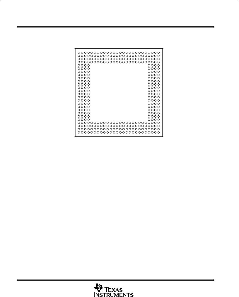
GNZ, GLS, and GNY BGA packages (bottom view)
GNZ 352-PIN BALL GRID ARRAY (BGA) PACKAGE (BOTTOM VIEW)
AF
AE
AD
AC
AB
AA
Y
W
V
U
T
R
P
N
M
L
K
J
H
G
F
E
D
C
B
A
1 |
3 |
5 |
7 |
9 |
11 |
13 |
15 |
17 |
19 |
21 |
23 |
25 |
||||||
2 |
4 |
|
6 |
8 |
10 |
12 |
14 |
16 |
18 |
20 |
22 |
24 |
26 |
|||||
4 |
POST OFFICE BOX 1443 • HOUSTON, TEXAS 77251–1443 |
TMS320C6203B
FIXED POINT DIGITAL SIGNAL PROCESSOR
SPRS086K – JANUARY 1999 – REVISED APRIL 2003
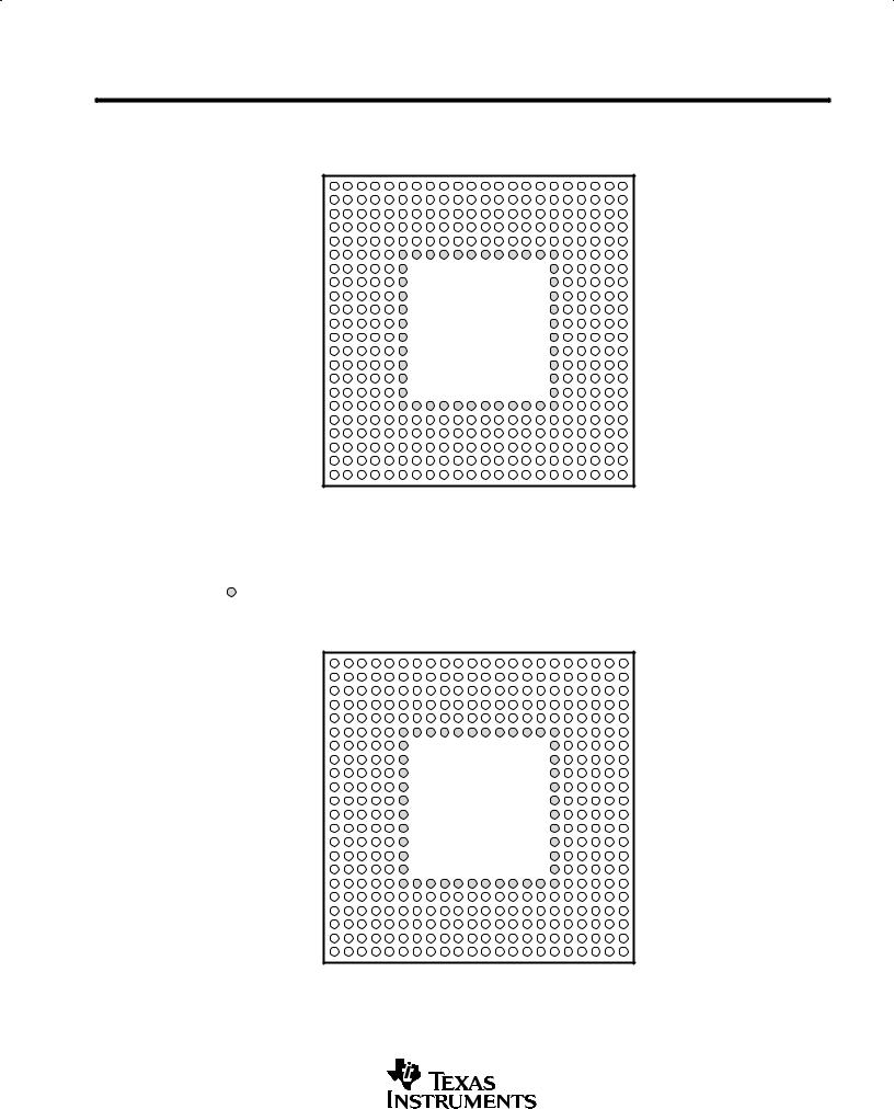
GNZ, GLS, and GNY BGA packages (bottom view) (continued)
GLS 384-PIN BGA PACKAGE (BOTTOM VIEW)
AB
AA
Y
W
V
U
T
R
P
N
M
L
K
J
H
G
F
E
D
C
B
A
1 |
3 |
5 |
7 |
9 |
|
11 |
13 |
15 |
17 |
19 |
21 |
|
2 |
4 |
6 |
8 |
10 |
12 |
14 |
16 |
18 |
20 |
22 |
The C6203B and C6202 GLS BGA packages are pin-compatible with the C6204 GLW package except that the inner row of balls (which are additional power and ground pins) are removed for the C6204 GLW package.
These balls are NOT applicable for the C6204 devices 340-pin GLW BGA package.
GNY 384-PIN BGA PACKAGE (BOTTOM VIEW)
AB
AA
Y
W
V
U
T
R
P
N
M
L
K
J
H
G
F
E
D
C
B
A
1 |
3 |
5 |
7 |
9 |
|
11 |
13 |
15 |
17 |
19 |
21 |
|
2 |
4 |
6 |
8 |
10 |
12 |
14 |
16 |
18 |
20 |
22 |
|
|
|
|
|
|
|
|
|
|
|
|
|
|
|
|
|
|
|
|
|
|
|
|
POST OFFICE BOX 1443 • HOUSTON, TEXAS 77251–1443 |
5 |