

TMS320C5x, TMS320LC5x
DIGITAL SIGNAL PROCESSORS
SPRS030A ± APRIL 1995 ± REVISED APRIL 1996
DPowerful 16-Bit TMS320C5x CPU
D20-, 25-, 35-, and 50-ns Single-Cycle Instruction Execution Time for 5-V Operation
D25-, 40-, and 50-ns Single-Cycle Instruction Execution Time for 3-V Operation
DSingle-Cycle 16 × 16-Bit Multiply/Add
D224K × 16-Bit Maximum Addressable
External Memory Space (64K Program, 64K Data, 64K I/O, and 32K Global)
D2K, 4K, 8K, 16K, 32K × 16-Bit Single-Access
On-Chip Program ROM
D1K, 3K, 6K, 9K × 16-Bit Single-Access
On-Chip Program/Data RAM (SARAM)
D1K Dual-Access On-Chip Program/Data RAM (DARAM)
DFull-Duplex Synchronous Serial Port for Coder/Decoder Interface
DTime-Division-Multiplexed (TDM) Serial Port
DHardware or Software Wait-State Generation Capability
DOn-Chip Timer for Control Operations
DRepeat Instructions for Efficient Use of Program Space
DBuffered Serial Port
DHost Port Interface
DMultiple Phase-Locked Loop (PLL) Clocking Options (×1, ×2, ×3, ×4, ×5, ×9
Depending on Device)
DBlock Moves for Data/Program Management
DOn-Chip Scan-Based Emulation Logic
DBoundary Scan
DFive Packaging Options
±100-Pin Quad Flat Package (PJ Suffix)
±100-Pin Thin Quad Flat Package (PZ Suffix)
±128-Pin Thin Quad Flat Package (PBK Suffix)
±132-Pin Quad Flat Package (PQ Suffix)
±144-Pin Thin Quad Flat Package (PGE Suffix)
DLow Power Dissipation and Power-Down Modes:
±47 mA (2.35 mA/MIP) at 5 V, 40-MHz Clock (Average)
±23 mA (1.15 mA/MIP) at 3 V, 40-MHz Clock (Average)
±10 mA at 5 V, 40-MHz Clock (IDLE1 Mode)
±3 mA at 5 V, 40-MHz Clock (IDLE2 Mode)
±5 µA at 5 V, Clocks Off (IDLE2 Mode)
DHigh-Performance Static CMOS Technology
DIEEE Standard 1149.1² Test-Access Port (JTAG)
description
The TMS320C5x generation of the Texas Instruments (TI ) TMS320 digital signal processors (DSPs) is fabricated with static CMOS integrated circuit technology; the architectural design is based upon that of an earlier TI DSP, the TMS320C25. The combination of advanced Harvard architecture, on-chip peripherals, on-chip memory, and a highly specialized instruction set is the basis of the operational flexibility and speed of the 'C5x³ devices. They execute up to 50 million instructions per second (MIPS).
The 'C5x devices offer these advantages:
DEnhanced TMS320 architectural design for increased performance and versatility
DModular architectural design for fast development of spin-off devices
DAdvanced integrated-circuit processing technology for increased performance
DUpward-compatible source code (source code for 'C1x and 'C2x DSPs is upward compatible with 'C5x DSPs.)
DEnhanced TMS320 instruction set for faster algorithms and for optimized high-level language operation
DNew static-design techniques for minimizing power consumption and maximizing radiation tolerance
Please be aware that an important notice concerning availability, standard warranty, and use in critical applications of Texas Instruments semiconductor products and disclaimers thereto appears at the end of this data sheet.
TI is a trademark of Texas Instruments Incorporated.
² IEEE Standard 1149.1±1990, IEEE Standard Test-Access Port and Boundary-Scan Architecture
³ References to 'C5x in this document include both TMS320C5x and TMS320LC5x devices unless specified otherwise.
PRODUCTION DATA information is current as of publication date. |
Copyright 1996, Texas Instruments Incorporated |
Products conform to specifications per the terms of Texas Instruments |
|
standard warranty. Production processing does not necessarily include |
|
testing of all parameters. |
|
POST OFFICE BOX 1443 •HOUSTON, TEXAS 77251±1443 |
1 |

TMS320C5x, TMS320LC5x
DIGITAL SIGNAL PROCESSORS
SPRS030A ± APRIL 1995 ± REVISED APRIL 1996
description (continued)
Table 1 provides a comparison of the devices in the 'C5x generation. It shows the capacity of on-chip RAM and ROM memories, number of serial and parallel I/O ports, execution time of one machine cycle, and type of package with total pin count.
Table 1. Characteristics of the 'C5x Processors
|
ON-CHIP MEMORY (16-BIT WORDS) |
I/O PORTS |
POWER |
CYCLE |
|
||||||
TMS320 |
|
|
|
|
|
PACKAGE |
|||||
|
DARAM |
SARAM |
ROM |
||||||||
|
|
|
SUPPLY |
TIME |
TYPE |
||||||
DEVICES |
|
|
|
|
|
|
|
||||
DATA |
DATA + |
DATA + |
PROG |
SERIAL |
² |
(V) |
(ns) |
QFP³ |
|||
|
|||||||||||
|
PROG |
PROG |
PARALLEL |
|
|
|
|||||
|
|
|
|
|
|
|
|
|
|||
|
|
|
|
|
|
|
|
|
|
|
|
TMS320C50 |
544 |
|
512 |
9K |
2K§ |
2 |
64K |
5 |
50/35/25 |
132 pin |
|
TMS320LC50 |
544 |
|
512 |
9K |
2K§ |
2 |
64K |
3.3 |
50/40/25 |
132 pin |
|
TMS320C51 |
544 |
|
512 |
1K |
8K§ |
2 |
64K |
5 |
50/35/25/20 |
100/132 pin |
|
TMS320LC51 |
544 |
|
512 |
1K |
8K§ |
2 |
64K |
3.3 |
50/40/25 |
100/132 pin |
|
TMS320C52 |
544 |
|
512 |
± |
4K§ |
1¶ |
64K |
5 |
50/35/25/20 |
100 pin |
|
TMS320LC52 |
544 |
|
512 |
± |
4K§ |
1¶ |
64K |
3.3 |
50/40/25 |
100 pin |
|
TMS320C53 |
544 |
|
512 |
3K |
16K§ |
2 |
64K |
5 |
50/35/25 |
132 pin |
|
TMS320LC53 |
544 |
|
512 |
3K |
16K§ |
2 |
64K |
3.3 |
50/40/25 |
132 pin |
|
TMS320C53S |
544 |
|
512 |
3K |
16K§ |
2 ¶ |
64K |
5 |
50/35/25 |
100 pin |
|
TMS320LC53S |
544 |
|
512 |
3K |
16K§ |
2 ¶ |
64K |
3.3 |
50/40/25 |
100 pin |
|
TMS320LC56 |
544 |
|
512 |
6K |
32K |
2 # |
64K |
3.3 |
35/25 |
100 pin |
|
TMS320LC57 |
544 |
|
512 |
6K |
32K |
2 # |
64K + HPI || |
3.3 |
35/25 |
128 pin |
|
TMS320C57S |
544 |
|
512 |
6K |
2K§ |
2 # |
64K + HPI || |
5 |
50/35/25 |
144 pin |
|
TMS320LC57S |
544 |
|
512 |
6K |
2K§ |
2 # |
64K + HPI || |
3.3 |
50/35 |
144 pin |
|
² Sixteen of the 64K parallel I/O ports are memory mapped. ³ QFP = Quad flatpack
§ ROM boot loader available
¶ TDM serial port not available
# Includes auto-buffered serial port (BSP) but TDM serial port not available || HPI = Host port interface
Pinouts for each package are device-specific.
2 |
POST OFFICE BOX 1443 •HOUSTON, TEXAS 77251±1443 |

TMS320C5x, TMS320LC5x
DIGITAL SIGNAL PROCESSORS
SPRS030A ± APRIL 1995 ± REVISED APRIL 1996
TMS320C50, TMS320LC50, TMS320C51, TMS320LC51, TMS320C53, TMS320LC53
PQ PACKAGE
( TOP VIEW )
|
|
|
|
|
|
NC |
|
NC |
|
V |
|
V |
|
D8 |
|
D9 |
|
D10 |
|
D11 |
|
D12 |
|
D13 |
|
D14 |
|
D15 |
|
MCMP/ |
|
V |
|
V |
|
TRST |
|
IAQ |
|
V |
V |
|
BIO |
|
HOLD |
|
READY |
|
RS |
|
TCLKR |
|
/TFSRTADD |
|
CLKX |
|
TCLKX |
|
TOUT |
|
V |
|
V |
|
EMU1/OFF |
|
EMU0 |
NC |
|
|||
|
|
|
|
|
|
|
|
|
|
|
|
|
|
|
|
|
|
|
|
|
|
|
|
|
|
|
|
|
|
|
|
|
|
|
|
|
||||||||||||||||||||||||||||||||||||
|
|
|
|
|
|
|
|
|
|
DDD |
|
DDD |
|
|
|
|
|
|
|
|
|
|
|
|
|
|
|
|
|
|
|
SSI |
|
SSI |
|
|
|
|
|
DDC |
DDC |
|
|
|
|
|
|
|
|
|
|
|
|
|
|
|
|
|
|
|
SSC |
|
SSC |
|
|
|
|
|
|
|
|
|
|
|
|
|
|
|
|
|
|
|
|
|
|
|
|
|
|
|
|
|
|
|
|
|
|
|
|
|
|
|
|
|
|
|
|
|
|
|
|
|
|
|
|
|
|
|
|
|
|
|
|
|
|
|
|
|
|
|
|
|
|
|
|
|
|||||||||
|
|
|
|
|
|
|
|
|
|
|
|
|
|
|
|
|
|
|
|
|
|
|
|
|
|
|
|
|
|
|
|
|
|
|
|
|
|
|
|
|
|
|
|
|
|
|
|
|
|
|
|
|
|
|
|
|
|
|
|
|
|
|
|
|||||||||
|
|
|
|
|
|
|
|
|
|
|
|
|
|
|
|
|
|
|
|
|
|
|
|
|
|
|
|
|
|
|
|
|
|
|
|
|
|
|
|
|
|
|
|
|
|
|
|
|
|
|
|
|
|
|
|
|
|
|
|
|
|
|
|
|
|
|
|
|
|
|
|
|
|
|
|
|
|
|
|
|
|
|
|
|
|
|
|
|
|
|
|
|
|
|
|
|
|
|
|
|
|
|
|
|
|
|
|
|
|
|
|
|
|
|
|
|
|
|
|
|
|
|
|
|
|
|
|
|
|
|
|
|
|
|
|
|
|
|
|
|
|
|
|
|
|
|
|
|
|
|
|
|
|
|
|
|
|
|
|
|
|
|
|
|
|
|
|
|
|
|
|
|
|
|
|
|
|
|
|
|
|
|
|
|
|
|
|
|
|
|
|
|
|
|
|
|
|
|
|
|
|
|
|
|
|
|
|
|
|
|
|
|
|
|
|
|
|
|
|
|
|
|
|
17 |
16 |
15 |
14 |
13 |
12 |
11 |
10 |
9 |
8 |
7 |
6 |
5 |
4 |
3 |
2 |
1 |
132 131 130 129 128 127 126 125 124 123 122 121 120 119 118 117 |
|
|
||||||||||||||||||||||||||||||||||||||||||||||||
|
|
|
|
|
|
|
|
|
|
|
|
|
|
|
|
|
|
|
|
|
|
|
|
|
|
|
|
|
|
|
|
|
|
|
|
|
|
|
|
|
|
|
|
|
|
|
|
|
|
|
|
|
|
|
|
|
|
|
|
|
|
|
|
|
|
|
|
|
|
|
|
|
|
NC |
|
18 |
|
|
|
|
|
|
|
|
|
|
|
|
|
|
|
|
|
|
|
|
|
|
|
|
|
|
|
|
|
|
|
|
|
|
|
|
|
|
|
|
|
|
|
|
|
|
|
|
|
|
|
|
|
|
|
|
|
|
|
|
|
|
|
|
116 |
|
|||
|
|
|
|
|
|
|
|
|
|
|
|
|
|
|
|
|
|
|
|
|
|
|
|
|
|
|
|
|
|
|
|
|
|
|
|
|
|
|
|
|
|
|
|
|
|
|
|
|
|
|
|
|
|
|
|
|
|
|
|
|
|
|
|
|
|
|
||||||
|
NC |
|
19 |
|
|
|
|
|
|
|
|
|
|
|
|
|
|
|
|
|
|
|
|
|
|
|
|
|
|
|
|
|
|
|
|
|
|
|
|
|
|
|
|
|
|
|
|
|
|
|
|
|
|
|
|
|
|
|
|
|
|
|
|
|
|
|
|
115 |
|
|||
|
|
|
|
|
|
|
|
|
|
|
|
|
|
|
|
|
|
|
|
|
|
|
|
|
|
|
|
|
|
|
|
|
|
|
|
|
|
|
|
|
|
|
|
|
|
|
|
|
|
|
|
|
|
|
|
|
|
|
|
|
|
|
|
|
|
|
||||||
VSSD |
|
20 |
|
|
|
|
|
|
|
|
|
|
|
|
|
|
|
|
|
|
|
|
|
|
|
|
|
|
|
|
|
|
|
|
|
|
|
|
|
|
|
|
|
|
|
|
|
|
|
|
|
|
|
|
|
|
|
|
|
|
|
|
|
|
|
|
114 |
|
||||
|
|
|
|
|
|
|
|
|
|
|
|
|
|
|
|
|
|
|
|
|
|
|
|
|
|
|
|
|
|
|
|
|
|
|
|
|
|
|
|
|
|
|
|
|
|
|
|
|
|
|
|
|
|
|
|
|
|
|
|
|
|
|
|
|
|
|||||||
VSSD |
|
21 |
|
|
|
|
|
|
|
|
|
|
|
|
|
|
|
|
|
|
|
|
|
|
|
|
|
|
|
|
|
|
|
|
|
|
|
|
|
|
|
|
|
|
|
|
|
|
|
|
|
|
|
|
|
|
|
|
|
|
|
|
|
|
|
|
113 |
|
||||
|
|
|
|
|
|
|
|
|
|
|
|
|
|
|
|
|
|
|
|
|
|
|
|
|
|
|
|
|
|
|
|
|
|
|
|
|
|
|
|
|
|
|
|
|
|
|
|
|
|
|
|
|
|
|
|
|
|
|
|
|
|
|
|
|
|
|||||||
|
NC |
|
22 |
|
|
|
|
|
|
|
|
|
|
|
|
|
|
|
|
|
|
|
|
|
|
|
|
|
|
|
|
|
|
|
|
|
|
|
|
|
|
|
|
|
|
|
|
|
|
|
|
|
|
|
|
|
|
|
|
|
|
|
|
|
|
|
|
112 |
|
|||
|
|
|
|
|
|
|
|
|
|
|
|
|
|
|
|
|
|
|
|
|
|
|
|
|
|
|
|
|
|
|
|
|
|
|
|
|
|
|
|
|
|
|
|
|
|
|
|
|
|
|
|
|
|
|
|
|
|
|
|
|
|
|
|
|
|
|
||||||
|
D7 |
|
23 |
|
|
|
|
|
|
|
|
|
|
|
|
|
|
|
|
|
|
|
|
|
|
|
|
|
|
|
|
|
|
|
|
|
|
|
|
|
|
|
|
|
|
|
|
|
|
|
|
|
|
|
|
|
|
|
|
|
|
|
|
|
|
|
|
111 |
|
|||
|
|
|
|
|
|
|
|
|
|
|
|
|
|
|
|
|
|
|
|
|
|
|
|
|
|
|
|
|
|
|
|
|
|
|
|
|
|
|
|
|
|
|
|
|
|
|
|
|
|
|
|
|
|
|
|
|
|
|
|
|
|
|
|
|
|
|
||||||
|
D6 |
|
24 |
|
|
|
|
|
|
|
|
|
|
|
|
|
|
|
|
|
|
|
|
|
|
|
|
|
|
|
|
|
|
|
|
|
|
|
|
|
|
|
|
|
|
|
|
|
|
|
|
|
|
|
|
|
|
|
|
|
|
|
|
|
|
|
|
110 |
|
|||
|
|
|
|
|
|
|
|
|
|
|
|
|
|
|
|
|
|
|
|
|
|
|
|
|
|
|
|
|
|
|
|
|
|
|
|
|
|
|
|
|
|
|
|
|
|
|
|
|
|
|
|
|
|
|
|
|
|
|
|
|
|
|
|
|
|
|
||||||
|
D5 |
|
25 |
|
|
|
|
|
|
|
|
|
|
|
|
|
|
|
|
|
|
|
|
|
|
|
|
|
|
|
|
|
|
|
|
|
|
|
|
|
|
|
|
|
|
|
|
|
|
|
|
|
|
|
|
|
|
|
|
|
|
|
|
|
|
|
|
109 |
|
|||
|
|
|
|
|
|
|
|
|
|
|
|
|
|
|
|
|
|
|
|
|
|
|
|
|
|
|
|
|
|
|
|
|
|
|
|
|
|
|
|
|
|
|
|
|
|
|
|
|
|
|
|
|
|
|
|
|
|
|
|
|
|
|
|
|
|
|
||||||
|
D4 |
|
26 |
|
|
|
|
|
|
|
|
|
|
|
|
|
|
|
|
|
|
|
|
|
|
|
|
|
|
|
|
|
|
|
|
|
|
|
|
|
|
|
|
|
|
|
|
|
|
|
|
|
|
|
|
|
|
|
|
|
|
|
|
|
|
|
|
108 |
|
|||
|
|
|
|
|
|
|
|
|
|
|
|
|
|
|
|
|
|
|
|
|
|
|
|
|
|
|
|
|
|
|
|
|
|
|
|
|
|
|
|
|
|
|
|
|
|
|
|
|
|
|
|
|
|
|
|
|
|
|
|
|
|
|
|
|
|
|
||||||
|
D3 |
|
27 |
|
|
|
|
|
|
|
|
|
|
|
|
|
|
|
|
|
|
|
|
|
|
|
|
|
|
|
|
|
|
|
|
|
|
|
|
|
|
|
|
|
|
|
|
|
|
|
|
|
|
|
|
|
|
|
|
|
|
|
|
|
|
|
|
107 |
|
|||
|
|
|
|
|
|
|
|
|
|
|
|
|
|
|
|
|
|
|
|
|
|
|
|
|
|
|
|
|
|
|
|
|
|
|
|
|
|
|
|
|
|
|
|
|
|
|
|
|
|
|
|
|
|
|
|
|
|
|
|
|
|
|
|
|
|
|
||||||
|
D2 |
|
28 |
|
|
|
|
|
|
|
|
|
|
|
|
|
|
|
|
|
|
|
|
|
|
|
|
|
|
|
|
|
|
|
|
|
|
|
|
|
|
|
|
|
|
|
|
|
|
|
|
|
|
|
|
|
|
|
|
|
|
|
|
|
|
|
|
106 |
|
|||
|
|
|
|
|
|
|
|
|
|
|
|
|
|
|
|
|
|
|
|
|
|
|
|
|
|
|
|
|
|
|
|
|
|
|
|
|
|
|
|
|
|
|
|
|
|
|
|
|
|
|
|
|
|
|
|
|
|
|
|
|
|
|
|
|
|
|
||||||
|
D1 |
|
29 |
|
|
|
|
|
|
|
|
|
|
|
|
|
|
|
|
|
|
|
|
|
|
|
|
|
|
|
|
|
|
|
|
|
|
|
|
|
|
|
|
|
|
|
|
|
|
|
|
|
|
|
|
|
|
|
|
|
|
|
|
|
|
|
|
105 |
|
|||
|
|
|
|
|
|
|
|
|
|
|
|
|
|
|
|
|
|
|
|
|
|
|
|
|
|
|
|
|
|
|
|
|
|
|
|
|
|
|
|
|
|
|
|
|
|
|
|
|
|
|
|
|
|
|
|
|
|
|
|
|
|
|
|
|
|
|
||||||
|
D0 |
|
30 |
|
|
|
|
|
|
|
|
|
|
|
|
|
|
|
|
|
|
|
|
|
|
|
|
|
|
|
|
|
|
|
|
|
|
|
|
|
|
|
|
|
|
|
|
|
|
|
|
|
|
|
|
|
|
|
|
|
|
|
|
|
|
|
|
104 |
|
|||
|
|
|
|
|
|
|
|
|
|
|
|
|
|
|
|
|
|
|
|
|
|
|
|
|
|
|
|
|
|
|
|
|
|
|
|
|
|
|
|
|
|
|
|
|
|
|
|
|
|
|
|
|
|
|
|
|
|
|
|
|
|
|
|
|
|
|
||||||
|
TMS |
|
31 |
|
|
|
|
|
|
|
|
|
|
|
|
|
|
|
|
|
|
|
|
|
|
|
|
|
|
|
|
|
|
|
|
|
|
|
|
|
|
|
|
|
|
|
|
|
|
|
|
|
|
|
|
|
|
|
|
|
|
|
|
|
|
|
|
103 |
|
|||
|
|
|
|
|
|
|
|
|
|
|
|
|
|
|
|
|
|
|
|
|
|
|
|
|
|
|
|
|
|
|
|
|
|
|
|
|
|
|
|
|
|
|
|
|
|
|
|
|
|
|
|
|
|
|
|
|
|
|
|
|
|
|
|
|
|
|
||||||
VDDD |
|
32 |
|
|
|
|
|
|
|
|
|
|
|
|
|
|
|
|
|
|
|
|
|
|
|
|
|
|
|
|
|
|
|
|
|
|
|
|
|
|
|
|
|
|
|
|
|
|
|
|
|
|
|
|
|
|
|
|
|
|
|
|
|
|
|
|
102 |
|
||||
|
|
|
|
|
|
|
|
|
|
|
|
|
|
|
|
|
|
|
|
|
|
|
|
|
|
|
|
|
|
|
|
|
|
|
|
|
|
|
|
|
|
|
|
|
|
|
|
|
|
|
|
|
|
|
|
|
|
|
|
|
|
|
|
|
|
|||||||
VDDD |
|
33 |
|
|
|
|
|
|
|
|
|
|
|
|
|
|
|
|
|
|
|
|
|
|
|
|
|
|
|
|
|
|
|
|
|
|
|
|
|
|
|
|
|
|
|
|
|
|
|
|
|
|
|
|
|
|
|
|
|
|
|
|
|
|
|
|
101 |
|
||||
|
|
|
|
|
|
|
|
|
|
|
|
|
|
|
|
|
|
|
|
|
|
|
|
|
|
|
|
|
|
|
|
|
|
|
|
|
|
|
|
|
|
|
|
|
|
|
|
|
|
|
|
|
|
|
|
|
|
|
|
|
|
|
|
|
|
|||||||
|
TCK |
|
34 |
|
|
|
|
|
|
|
|
|
|
|
|
|
|
|
|
|
|
|
|
|
|
|
|
|
|
|
|
|
|
|
|
|
|
|
|
|
|
|
|
|
|
|
|
|
|
|
|
|
|
|
|
|
|
|
|
|
|
|
|
|
|
|
|
100 |
|
|||
|
|
|
|
|
|
|
|
|
|
|
|
|
|
|
|
|
|
|
|
|
|
|
|
|
|
|
|
|
|
|
|
|
|
|
|
|
|
|
|
|
|
|
|
|
|
|
|
|
|
|
|
|
|
|
|
|
|
|
|
|
|
|
|
|
|
|
||||||
VSSD |
|
35 |
|
|
|
|
|
|
|
|
|
|
|
|
|
|
|
|
|
|
|
|
|
|
|
|
|
|
|
|
|
|
|
|
|
|
|
|
|
|
|
|
|
|
|
|
|
|
|
|
|
|
|
|
|
|
|
|
|
|
|
|
|
|
|
|
99 |
|
||||
|
|
|
|
|
|
|
|
|
|
|
|
|
|
|
|
|
|
|
|
|
|
|
|
|
|
|
|
|
|
|
|
|
|
|
|
|
|
|
|
|
|
|
|
|
|
|
|
|
|
|
|
|
|
|
|
|
|
|
|
|
|
|
|
|
|
|||||||
VSSD |
|
36 |
|
|
|
|
|
|
|
|
|
|
|
|
|
|
|
|
|
|
|
|
|
|
|
|
|
|
|
|
|
|
|
|
|
|
|
|
|
|
|
|
|
|
|
|
|
|
|
|
|
|
|
|
|
|
|
|
|
|
|
|
|
|
|
|
98 |
|
||||
|
|
|
|
|
|
|
|
|
|
|
|
|
|
|
|
|
|
|
|
|
|
|
|
|
|
|
|
|
|
|
|
|
|
|
|
|
|
|
|
|
|
|
|
|
|
|
|
|
|
|
|
|
|
|
|
|
|
|
|
|
|
|
|
|
|
|||||||
|
NC |
|
37 |
|
|
|
|
|
|
|
|
|
|
|
|
|
|
|
|
|
|
|
|
|
|
|
|
|
|
|
|
|
|
|
|
|
|
|
|
|
|
|
|
|
|
|
|
|
|
|
|
|
|
|
|
|
|
|
|
|
|
|
|
|
|
|
|
97 |
|
|||
|
|
|
|
|
|
|
|
|
|
|
|
|
|
|
|
|
|
|
|
|
|
|
|
|
|
|
|
|
|
|
|
|
|
|
|
|
|
|
|
|
|
|
|
|
|
|
|
|
|
|
|
|
|
|
|
|
|
|
|
|
|
|
|
|
|
|
||||||
|
|
|
|
|
|
|
|
|
|
|
|
|
|
|
|
|
|
|
|
|
|
|
|
|
|
|
|
|
|
|
|
|
|
|
|
|
|
|
|
|
|
|
|
|
|
|
|
|
|
|
|
|
|
|
|
|
|
|
|
|
|
|
|
|
|
|
|
|
|
|
|
|
|
INT1 |
|
|
|
38 |
|
|
|
|
|
|
|
|
|
|
|
|
|
|
|
|
|
|
|
|
|
|
|
|
|
|
|
|
|
|
|
|
|
|
|
|
|
|
|
|
|
|
|
|
|
|
|
|
|
|
|
|
|
|
|
|
|
|
|
|
|
|
|
|
96 |
|
|
|
|
|
|
|
|
|
|
|
|
|
|
|
|
|
|
|
|
|
|
|
|
|
|
|
|
|
|
|
|
|
|
|
|
|
|
|
|
|
|
|
|
|
|
|
|
|
|
|
|
|
|
|
|
|
|
|
|
|
|
|
|
|
|
|
|
|
|
|
||||
|
|
|
|
|
|
|
|
|
|
|
|
|
|
|
|
|
|
|
|
|
|
|
|
|
|
|
|
|
|
|
|
|
|
|
|
|
|
|
|
|
|
|
|
|
|
|
|
|
|
|
|
|
|
|
|
|
|
|
|
|
|
|
|
|
|
|
|
|
|
|
|
|
|
|
|
|
|
|
|
|
|
|
|
|
|
|
|
|
|
|
|
|
|
|
|
|
|
|
|
|
|
|
|
|
|
|
|
|
|
|
|
|
|
|
|
|
|
|
|
|
|
|
|
|
|
|
|
|
|
|
|
|
|
|
|
|
|
|
|
|
|
|
|
|
|
|
INT2 |
|
|
|
39 |
|
|
|
|
|
|
|
|
|
|
|
|
|
|
|
|
|
|
|
|
|
|
|
|
|
|
|
|
|
|
|
|
|
|
|
|
|
|
|
|
|
|
|
|
|
|
|
|
|
|
|
|
|
|
|
|
|
|
|
|
|
|
|
|
95 |
|
|
|
|
|
|
|
|
|
|
|
|
|
|
|
|
|
|
|
|
|
|
|
|
|
|
|
|
|
|
|
|
|
|
|
|
|
|
|
|
|
|
|
|
|
|
|
|
|
|
|
|
|
|
|
|
|
|
|
|
|
|
|
|
|
|
|
|
|
|
|
|
|
|
|
|
INT3 |
|
|
|
40 |
|
|
|
|
|
|
|
|
|
|
|
|
|
|
|
|
|
|
|
|
|
|
|
|
|
|
|
|
|
|
|
|
|
|
|
|
|
|
|
|
|
|
|
|
|
|
|
|
|
|
|
|
|
|
|
|
|
|
|
|
|
|
|
|
94 |
|
|
|
|
|
|
|
|
|
|
|
|
|
|
|
|
|
|
|
|
|
|
|
|
|
|
|
|
|
|
|
|
|
|
|
|
|
|
|
|
|
|
|
|
|
|
|
|
|
|
|
|
|
|
|
|
|
|
|
|
|
|
|
|
|
|
|
|
|
|
|
|
|
|
|
|
INT4 |
|
|
|
41 |
|
|
|
|
|
|
|
|
|
|
|
|
|
|
|
|
|
|
|
|
|
|
|
|
|
|
|
|
|
|
|
|
|
|
|
|
|
|
|
|
|
|
|
|
|
|
|
|
|
|
|
|
|
|
|
|
|
|
|
|
|
|
|
|
93 |
|
|
|
|
|
|
|
|
|
|
|
|
|
|
|
|
|
|
|
|
|
|
|
|
|
|
|
|
|
|
|
|
|
|
|
|
|
|
|
|
|
|
|
|
|
|
|
|
|
|
|
|
|
|
|
|
|
|
|
|
|
|
|
|
|
|
|
|
|
|
|
|
|
|
|
|
NMI |
|
|
42 |
|
|
|
|
|
|
|
|
|
|
|
|
|
|
|
|
|
|
|
|
|
|
|
|
|
|
|
|
|
|
|
|
|
|
|
|
|
|
|
|
|
|
|
|
|
|
|
|
|
|
|
|
|
|
|
|
|
|
|
|
|
|
|
|
92 |
|
||
|
DR |
|
43 |
|
|
|
|
|
|
|
|
|
|
|
|
|
|
|
|
|
|
|
|
|
|
|
|
|
|
|
|
|
|
|
|
|
|
|
|
|
|
|
|
|
|
|
|
|
|
|
|
|
|
|
|
|
|
|
|
|
|
|
|
|
|
|
|
91 |
|
|||
|
|
|
|
|
|
|
|
|
|
|
|
|
|
|
|
|
|
|
|
|
|
|
|
|
|
|
|
|
|
|
|
|
|
|
|
|
|
|
|
|
|
|
|
|
|
|
|
|
|
|
|
|
|
|
|
|
|
|
|
|
|
|
|
|
|
|
||||||
|
|
|
|
|
|
|
|
|
|
|
|
|
|
|
|
|
|
|
|
|
|
|
|
|
|
|
|
|
|
|
|
|
|
|
|
|
|
|
|
|
|
|
|
|
|
|
|
|
|
|
|
|
|
|
|
|
|
|
|
|
|
|
|
|
|
|
||||||
|
TDR |
|
44 |
|
|
|
|
|
|
|
|
|
|
|
|
|
|
|
|
|
|
|
|
|
|
|
|
|
|
|
|
|
|
|
|
|
|
|
|
|
|
|
|
|
|
|
|
|
|
|
|
|
|
|
|
|
|
|
|
|
|
|
|
|
|
|
|
90 |
|
|||
|
|
|
|
|
|
|
|
|
|
|
|
|
|
|
|
|
|
|
|
|
|
|
|
|
|
|
|
|
|
|
|
|
|
|
|
|
|
|
|
|
|
|
|
|
|
|
|
|
|
|
|
|
|
|
|
|
|
|
|
|
|
|
|
|
|
|
||||||
|
|
|
|
|
|
|
|
|
|
|
|
|
|
|
|
|
|
|
|
|
|
|
|
|
|
|
|
|
|
|
|
|
|
|
|
|
|
|
|
|
|
|
|
|
|
|
|
|
|
|
|
|
|
|
|
|
|
|
|
|
|
|
|
|
|
|
||||||
|
FSR |
|
45 |
|
|
|
|
|
|
|
|
|
|
|
|
|
|
|
|
|
|
|
|
|
|
|
|
|
|
|
|
|
|
|
|
|
|
|
|
|
|
|
|
|
|
|
|
|
|
|
|
|
|
|
|
|
|
|
|
|
|
|
|
|
|
|
|
89 |
|
|||
|
|
|
|
|
|
|
|
|
|
|
|
|
|
|
|
|
|
|
|
|
|
|
|
|
|
|
|
|
|
|
|
|
|
|
|
|
|
|
|
|
|
|
|
|
|
|
|
|
|
|
|
|
|
|
|
|
|
|
|
|
|
|
|
|
|
|
||||||
|
|
|
|
|
|
|
|
|
|
|
|
|
|
|
|
|
|
|
|
|
|
|
|
|
|
|
|
|
|
|
|
|
|
|
|
|
|
|
|
|
|
|
|
|
|
|
|
|
|
|
|
|
|
|
|
|
|
|
|
|
|
|
|
|
|
|
||||||
CLKR |
|
46 |
|
|
|
|
|
|
|
|
|
|
|
|
|
|
|
|
|
|
|
|
|
|
|
|
|
|
|
|
|
|
|
|
|
|
|
|
|
|
|
|
|
|
|
|
|
|
|
|
|
|
|
|
|
|
|
|
|
|
|
|
|
|
|
|
88 |
|
||||
|
|
|
|
|
|
|
|
|
|
|
|
|
|
|
|
|
|
|
|
|
|
|
|
|
|
|
|
|
|
|
|
|
|
|
|
|
|
|
|
|
|
|
|
|
|
|
|
|
|
|
|
|
|
|
|
|
|
|
|
|
|
|
|
|
|
|||||||
|
|
|
|
|
|
|
|
|
|
|
|
|
|
|
|
|
|
|
|
|
|
|
|
|
|
|
|
|
|
|
|
|
|
|
|
|
|
|
|
|
|
|
|
|
|
|
|
|
|
|
|
|
|
|
|
|
|
|
|
|
|
|
|
|
|
|||||||
VDDA |
|
47 |
|
|
|
|
|
|
|
|
|
|
|
|
|
|
|
|
|
|
|
|
|
|
|
|
|
|
|
|
|
|
|
|
|
|
|
|
|
|
|
|
|
|
|
|
|
|
|
|
|
|
|
|
|
|
|
|
|
|
|
|
|
|
|
|
87 |
|
||||
|
|
|
|
|
|
|
|
|
|
|
|
|
|
|
|
|
|
|
|
|
|
|
|
|
|
|
|
|
|
|
|
|
|
|
|
|
|
|
|
|
|
|
|
|
|
|
|
|
|
|
|
|
|
|
|
|
|
|
|
|
|
|
|
|
|
|||||||
VDDA |
|
48 |
|
|
|
|
|
|
|
|
|
|
|
|
|
|
|
|
|
|
|
|
|
|
|
|
|
|
|
|
|
|
|
|
|
|
|
|
|
|
|
|
|
|
|
|
|
|
|
|
|
|
|
|
|
|
|
|
|
|
|
|
|
|
|
|
86 |
|
||||
|
|
|
|
|
|
|
|
|
|
|
|
|
|
|
|
|
|
|
|
|
|
|
|
|
|
|
|
|
|
|
|
|
|
|
|
|
|
|
|
|
|
|
|
|
|
|
|
|
|
|
|
|
|
|
|
|
|
|
|
|
|
|
|
|
|
|||||||
|
NC |
|
49 |
|
|
|
|
|
|
|
|
|
|
|
|
|
|
|
|
|
|
|
|
|
|
|
|
|
|
|
|
|
|
|
|
|
|
|
|
|
|
|
|
|
|
|
|
|
|
|
|
|
|
|
|
|
|
|
|
|
|
|
|
|
|
|
|
85 |
|
|||
|
|
|
|
|
|
|
|
|
|
|
|
|
|
|
|
|
|
|
|
|
|
|
|
|
|
|
|
|
|
|
|
|
|
|
|
|
|
|
|
|
|
|
|
|
|
|
|
|
|
|
|
|
|
|
|
|
|
|
|
|
|
|
|
|
|
|
||||||
|
NC |
|
50 |
|
|
|
|
|
|
|
|
|
|
|
|
|
|
|
|
|
|
|
|
|
|
|
|
|
|
|
|
|
|
|
|
|
|
|
|
|
|
|
|
|
|
|
|
|
|
|
|
|
|
|
|
|
|
|
|
|
|
|
|
|
|
|
|
84 |
|
|||
|
|
|
|
|
|
|
|
|
|
|
|
|
|
|
|
|
|
|
|
|
|
|
|
|
|
|
|
|
|
|
|
|
|
|
|
|
|
|
|
|
|
|
|
|
|
|
|
|
|
|
|
|
|
|
|
|
|
|
|
|
|
|
|
|
|
|
||||||
|
|
|
|
|
51 |
52 |
53 |
54 |
55 |
56 |
57 |
58 |
59 |
60 |
61 |
62 |
63 |
64 |
65 |
66 |
67 |
68 |
|
69 |
70 |
71 |
72 |
73 |
74 |
75 |
76 |
77 |
78 |
79 |
80 |
81 |
82 |
|
83 |
|
|
|||||||||||||||||||||||||||||||
|
|
|
|
|
|
|
|
|
|
|
|
|
|
|
|
|
|
|
|
|
|
|
|
|
|
|
|
|
|
|
|
|
|
|
|
|
|
|
|
|
|
|
|
|
|
|
|
|
|
|
|
|
|
|
|
|
|
|
|
|
|
|
|
|
|
|
|
|
|
|
|
|
|
|
|
|
|
|
|
|
|
|
|
|
|
|
|
|
|
|
|
|
|
|
|
|
|
|
|
|
|
|
|
|
|
|
|
|
|
|
|
|
|
|
|
|
|
|
|
|
|
|
|
|
|
|
|
|
|
|
|
|
|
|
|
|
|
|
|
|
|
|
|
|
|
|
|
|
|
|
|
NC |
|
NC |
|
V |
|
V |
|
A0 |
|
A1 |
|
A2 |
|
A3 |
|
A4 |
|
A5 |
|
A6 |
|
A7 |
|
A8 |
|
A9 |
|
V |
|
V |
|
TDI |
|
V |
V |
|
NC |
|
CLKMD1 |
|
A10 |
|
A11 |
|
A12 |
|
A13 |
|
A14 |
|
A15 |
|
NC |
|
NC |
|
V |
|
V |
|
RD |
WE |
|
|||
|
|
|
|
|
|
|
|
|
|
SSA |
|
SSA |
|
|
|
|
|
|
|
|
|
|
|
|
|
|
|
|
|
|
|
|
|
DDI |
|
DDI |
|
|
|
SSA |
SSA |
|
|
|
|
|
|
|
|
|
|
|
|
|
|
|
|
|
|
|
|
|
DDA |
|
DDA |
|
|
|
|
|
|
|
|
|
|
|
|
|
|
|
|
|
|
|
|
|
|
|
|
|
|
|
|
|
|
|
|
|
|
|
|
|
|
|
|
|
|
|
|
|
|
|
|
|
|
|
|
|
|
|
|
|
|
|
|
|
|
|
|
|
|
|
|
||||||||||||
NC
NC
VDDI
VDDI
IACK
NC CLKOUT1 XF
HOLDA
TDX
DX
TFSX / TFRM FSX CLKMD2 VSSI
VSSI
TDO
VDDC
VDDC
X1
X2 / CLKIN CLKIN2
BR
STRB
R/ W
PS
IS
DS
NC
VSSC
VSSC
NC
NC
NOTE: NC = No connect (These pins are reserved.)
POST OFFICE BOX 1443 •HOUSTON, TEXAS 77251±1443 |
3 |

TMS320C5x, TMS320LC5x
DIGITAL SIGNAL PROCESSORS
SPRS030A ± APRIL 1995 ± REVISED APRIL 1996
|
|
|
|
|
|
|
|
|
|
|
|
|
|
|
|
|
|
|
|
|
|
|
|
|
|
Pin Functions for Devices in the PQ Package |
|
|
|
|
|
|
|
|
|
|
|
|
|
|
|
SIGNAL |
|
TYPE |
|
DESCRIPTION |
|||||||||
|
|
|
|
|
|
|
|
|
|
|
|
|
|
|
|
|
|
|
|
|
|
|
|
|
|
|
|
|
|
|
|
|
|
|
|
|
|
|
|
|
|
|
|
|
|
|
|
|
|
|
|
|
|
|
PARALLEL INTERFACE BUS |
|
|
|
|
|
|
|
|
|
|
|
|
|
|
|
|
|
|
|
|
|
|
|
|
|
|
|
|
|
A0 ± A15 |
|
I / O / Z |
|
16-bit external address bus (MSB: A15, LSB: A0) |
||||||||||||||||||||||
|
|
|
|
|
|
|
|
|
|
|
|
|
|
|
|
|
|
|
|
|
|
|
|
|
|
|
|
|
D0 ± D15 |
|
I / O / Z |
|
16-bit external data bus (MSB: D15, LSB: D0) |
||||||||||||||||||||||
|
|
|
|
|
|
|
|
|
|
|
|
|
|
|
|
|
|
|
|
|
|
|
|
|
|
|
|
|
|
|
|
|
|
|
|
|
|
|
|
|
|
|
|
|
|
|
|
|
|
|
|
|
O / Z |
|
Program, data, and I /O space select outputs, respectively |
|
PS, |
|
|
|
|
|
|
DS, |
|
|
|
|
IS |
|
|
|
|
||||||||||
|
|
|
|
|
|
|
|
|
|
|
|
|
|
|
|
|
|
|
|
|
|
|
|
|
|||
|
|
|
|
|
|
|
|
|
|
|
|
|
|
|
|
|
|
|
|
|
|
|
|
|
I / O / Z |
|
Timing strobe for external cycles and external DMA |
|
STRB |
|
|
|
|
|
|
|
|
|
|
|
|||||||||||||||
|
|
|
|
|
|
|
|
|
|
|
|
|
|
|
|
|
|
|
|
|
|
|
|||||
|
R / |
|
|
|
|
|
|
|
|
|
|
|
|
|
|
|
|
|
|
|
|
|
|
|
I / O / Z |
|
Read/ write select for external cycles and external DMA |
|
W |
|
|
|
|
|
|
|
|
|
|
|
|
||||||||||||||
|
|
|
|
|
|
|
|
|
|
|
|
|
|
|
|
|
|
|
|
|
|
||||||
|
|
|
|
|
|
|
|
|
|
|
|
|
|
|
|
|
|
|
|
|
|
|
|
|
O / Z |
|
Read and write strobes, respectively, for external cycles |
|
RD, |
|
|
|
|
|
WE |
|
|
|
|
|
|
||||||||||||||
|
|
|
|
|
|
|
|
|
|
|
|
|
|
|
|
|
|
|
|
|
|||||||
|
READY |
|
|
|
|
|
I |
|
External bus ready/ wait-state control input |
||||||||||||||||||
|
|
|
|
|
|
|
|
|
|
|
|
|
|
|
|
|
|
|
|
||||||||
|
|
|
|
|
|
|
|
|
|
|
|
|
|
|
|
|
|
|
|
|
|
|
|
|
I / O / Z |
|
Bus request. Arbitrates global memory and external DMA |
|
BR |
|
|
|
|
|
|
|
|
|
|
|
|
|
|
|
|
|
|||||||||
|
|
|
|
|
|
|
|
|
|
|
|
|
|
|
|
|
|
|
|
|
|
|
|
|
|
|
|
|
|
|
|
|
|
|
|
|
|
|
|
|
|
|
|
|
|
|
|
|
|
|
|
|
|
|
SYSTEM INTERFACE / CONTROL SIGNALS |
|
|
|
|
|
|
|
|
|
|
|
|
|
|
|
|
|
|
|
|
||||||||
|
RS |
|
|
|
|
|
|
|
|
|
|
|
|
|
|
|
|
I |
|
Reset. Initializes device and sets PC to zero |
|||||||
|
|
|
|
|
|
|
|
|
|
|
|
|
|
|
|
|
|
||||||||||
|
|
|
|
|
|
|
|
|
|
|
|
|
|
|
|
|
|
|
|
|
|
|
|
|
I |
|
Microprocessor/microcomputer mode select. Enables internal ROM |
|
MP/MC |
|
|
|
|
|
|
|
|||||||||||||||||||
|
|
|
|
|
|
|
|
|
|
|
|
|
|
|
|
|
|||||||||||
|
|
|
|
|
|
|
|
|
|
|
|
|
|
|
|
|
|
|
|
|
|
|
|
|
I |
|
Puts parallel I/ F bus in high-impedance state after current cycle |
|
HOLD |
|
|
|
|
|
|
|
|
|
|||||||||||||||||
|
|
|
|
|
|
|
|
|
|
|
|
|
|
|
|
||||||||||||
|
|
|
|
|
|
|
|
|
|
|
|
|
|
|
|
|
|
|
|
|
|
|
|
|
O / Z |
|
Hold acknowledge. Indicates external bus in hold state |
|
HOLDA |
|
|
|
|
|
|
|
|||||||||||||||||||
|
|
|
|
|
|
|
|
|
|
|
|
|
|
|
|
||||||||||||
|
XF |
|
|
|
|
|
O / Z |
|
External flag output. Set /cleared through software |
||||||||||||||||||
|
|
|
|
|
|
|
|
|
|
|
|
|
|
|
|||||||||||||
|
|
|
|
|
|
|
|
|
|
|
|
|
|
|
|
|
|
|
|
|
|
|
|
|
I |
|
I /O branch input. Implements conditional branches |
|
BIO |
|
|
|
|
|
|
|
|
|
|
|
|
||||||||||||||
|
|
|
|
|
|
|
|
|
|
|
|
|
|
|
|||||||||||||
|
TOUT |
|
|
|
|
|
O / Z |
|
Timer output signal. Indicates output of internal timer |
||||||||||||||||||
|
|
|
|
|
|
|
|
|
|
|
|
|
|
||||||||||||||
|
|
|
|
|
|
|
|
|
|
|
|
|
|
|
|
|
|
|
|
|
|
|
|
|
O / Z |
|
Instruction acquisition signal |
|
IAQ |
|
|
|
|
|
|
|
|
|
|
|
|||||||||||||||
|
|
|
|
|
|
|
|
|
|
|
|
|
|||||||||||||||
|
|
|
|
|
|
|
|
|
|
|
|
|
|
|
|
|
|
|
|
|
|
|
|
|
O / Z |
|
Interrupt acknowledge signal |
|
IACK |
|
|
|
|
|
|
|
|
||||||||||||||||||
|
|
|
|
|
|
|
|
|
|||||||||||||||||||
|
|
|
|
|
|
|
|
|
|
|
± |
|
|
|
|
|
|
|
|
|
I |
|
External interrupt inputs |
||||
|
INT1 |
INT4 |
|
|
|
||||||||||||||||||||||
|
|
|
|
|
|
|
|
|
|
||||||||||||||||||
|
|
|
|
|
|
|
|
|
|
|
|
|
|
|
|
|
|
|
|
|
|
|
|
|
I |
|
Nonmaskable external interrupt |
|
NMI |
|
|
|
|
|
|
|
|||||||||||||||||||
|
|
|
|
|
|
|
|
|
|
|
|
|
|
|
|
|
|
|
|
|
|
|
|
|
|
|
|
|
|
|
|
|
|
|
|
|
|
|
|
|
|
|
|
|
|
|
|
|
|
|
|
|
|
|
SERIAL PORT INTERFACE (SPI) |
|
|
|
|
|
|
|
|
|
|
||||||||||||||||||
|
DR |
|
|
|
|
|
I |
|
Serial receive-data input |
||||||||||||||||||
|
|
|
|
|
|
|
|
|
|
||||||||||||||||||
|
DX |
|
|
|
|
|
O / Z |
|
Serial transmit-data output. In high-impedance state when not transmitting |
||||||||||||||||||
|
|
|
|
|
|
|
|
|
|
||||||||||||||||||
|
CLKR |
|
|
|
|
|
I |
|
Serial receive-data clock input |
||||||||||||||||||
|
|
|
|
|
|
|
|
|
|
||||||||||||||||||
|
CLKX |
|
|
|
|
|
I / O / Z |
|
Serial transmit-data clock. Internal or external source |
||||||||||||||||||
|
|
|
|
|
|
|
|
|
|
||||||||||||||||||
|
FSR |
|
|
|
|
|
I |
|
Serial receive-frame-synchronization input |
||||||||||||||||||
|
|
|
|
|
|
|
|
|
|
||||||||||||||||||
|
FSX |
|
|
|
|
|
I / O / Z |
|
Serial transmit-frame-synchronization signal. Internal or external source |
||||||||||||||||||
|
|
|
|
|
|
|
|
|
|
|
|
|
|
|
|
|
|
|
|
|
|
|
|
|
|
|
|
|
|
|
|
|
|
|
|
|
|
|
|
|
|
|
|
|
|
|
|
|
|
|
|
|
|
|
TDM SERIAL-PORT INTERFACE |
|
|
|
|
|
|
|
|
|
|
||||||||||||||||||
|
TDR |
|
|
|
|
|
I |
|
TDM serial receive-data input |
||||||||||||||||||
|
|
|
|
|
|
|
|
|
|
||||||||||||||||||
|
TDX |
|
|
|
|
|
O / Z |
|
TDM serial transmit-data output. In high-impedance state when not transmitting |
||||||||||||||||||
|
|
|
|
|
|
|
|
|
|
||||||||||||||||||
|
TCLKR |
|
|
|
|
|
I |
|
TDM serial receive-data clock input |
||||||||||||||||||
|
|
|
|
|
|
|
|
|
|
||||||||||||||||||
|
TCLKX |
|
|
|
|
|
I / O / Z |
|
TDM serial transmit-data clock. Internal or external source |
||||||||||||||||||
|
|
|
|
|
|
|
|
|
|
|
|
|
|
|
|
|
|
|
|
|
|
|
|
|
|
|
|
|
TFSR / TADD |
|
I / O / Z |
|
TDM serial receive-frame-synchronization input. In the TDM mode, TFSR / TADD is used to output / |
||||||||||||||||||||||
|
|
|
input the address of the port. |
||||||||||||||||||||||||
|
|
|
|
|
|
|
|
|
|
|
|
|
|
|
|
|
|
|
|
|
|
|
|
|
|
|
|
|
|
|
|
|
|
|
|
|
|
|
|
|
|
|
|
|
|
|
|
|
|
|
|
|
|
|
|
|
TFSX / TFRM |
|
I |
|
TDM serial transmit-frame-synchronization signal. Internal or external source. In the TDM mode, |
||||||||||||||||||||||
|
|
|
TFSX / TFRM becomes TFRM, the TDM frame synchronization. |
||||||||||||||||||||||||
|
|
|
|
|
|
|
|
|
|
|
|
|
|
|
|
|
|
|
|
|
|
|
|
|
|
|
|
LEGEND: |
|
|
|
||||||||||||||||||||||||
|
I = |
Input |
|
|
|
||||||||||||||||||||||
|
O = |
Output |
|
|
|
||||||||||||||||||||||
|
Z = |
High impedance |
|
|
|
||||||||||||||||||||||
4 |
POST OFFICE BOX 1443 •HOUSTON, TEXAS 77251±1443 |

TMS320C5x, TMS320LC5x
DIGITAL SIGNAL PROCESSORS
SPRS030A ± APRIL 1995 ± REVISED APRIL 1996
|
|
|
|
|
|
|
Pin Functions for Devices in the PQ Package (Continued) |
||
|
|
|
|
|
|
|
|
EMULATION/IEEE STANDARD 1149.1 TEST ACCESS PORT (TAP) |
|
|
|
|
|
|
|
|
|
|
|
|
TDI |
|
|
|
I |
|
TAP scan data input |
||
|
|
|
|
|
|
|
|
|
|
|
TDO |
|
|
|
O / Z |
|
TAP scan data output |
||
|
|
|
|
|
|
|
|
|
|
|
TMS |
|
|
|
I |
|
TAP mode select input |
||
|
|
|
|
|
|
|
|
|
|
|
TCK |
|
|
|
I |
|
TAP clock input |
||
|
|
|
|
|
|
|
|
|
|
|
|
|
|
|
|
|
I |
|
TAP reset (with pulldown resistor). Disables TAP when low |
|
TRST |
|
|
|
|
|
|
||
|
|
|
|
|
|
|
|
|
|
|
EMU0 |
|
|
|
I / O / Z |
|
Emulation control 0. Reserved for emulation use |
||
|
|
|
|
|
|
||||
|
EMU1/ |
|
|
|
|
I / O / Z |
|
Emulation control 1. Puts outputs in high-impedance state when low |
|
|
OFF |
|
|
|
|||||
|
|
|
|
|
|
|
|
|
|
|
|
|
|
|
|
|
|
|
CLOCK GENERATION AND CONTROL |
|
|
|
|
|
|
|
|
||
|
X1 |
|
|
|
O |
|
Oscillator output |
||
|
|
|
|
|
|
||||
|
X2 / CLKIN |
|
I |
|
Clock/oscillator input |
||||
|
|
|
|
|
|
|
|
||
|
CLKIN2 |
|
|
|
I |
|
Clock input |
||
|
|
|
|
|
|
||||
|
CLKMD1, CLKMD2 |
|
I |
|
Clock-mode select inputs |
||||
|
|
|
|
|
|
||||
|
CLKOUT1 |
|
O / Z |
|
Device system-clock output |
||||
|
|
|
|
|
|
|
|
|
|
|
|
|
|
|
|
|
|
|
POWER SUPPLY CONNECTIONS |
|
|
|
|
|
|
|
|
||
|
VDDA |
|
|
|
S |
|
Supply connection, address-bus output |
||
|
VDDD |
|
|
|
S |
|
Supply connection, data-bus output |
||
|
VDDC |
|
|
|
S |
|
Supply connection, control output |
||
|
VDDI |
|
|
|
S |
|
Supply connection, internal logic |
||
|
VSSA |
|
|
|
S |
|
Supply connection, address-bus output |
||
|
VSSD |
|
|
|
S |
|
Supply connection, data-bus output |
||
|
VSSC |
|
|
|
S |
|
Supply connection, control output |
||
|
VSSI |
|
|
|
S |
|
Supply connection, internal logic |
||
LEGEND: |
|
|
|
||||||
|
I = |
Input |
|
|
|
||||
|
O = |
Output |
|
|
|
||||
|
S = |
Supply |
|
|
|
||||
|
Z = |
High impedance |
|
|
|
||||
POST OFFICE BOX 1443 •HOUSTON, TEXAS 77251±1443 |
5 |
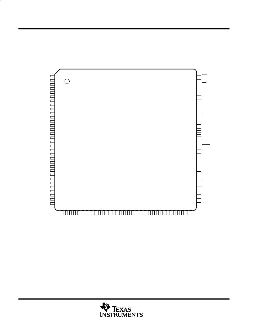
TMS320C5x, TMS320LC5x
DIGITAL SIGNAL PROCESSORS
SPRS030A ± APRIL 1995 ± REVISED APRIL 1996
TMS320LC57 PBK PACKAGE ( TOP VIEW )
V |
V |
V |
CLKOUT1 XF |
|
HOLDA BDX DX |
HD7 BFSX HD6 FSX HD5 |
CLKMD2 HD4 |
|
V |
V |
TDO V |
X1 X2/CLKIN |
|
CLKMD3 BR HD3 |
|
STRB |
|
W/R PS |
IS DS |
HD2 V |
V |
|||||||||||||||||||||||||||||||||||||||||||
|
|
|
|
|
||||||||||||||||||||||||||||||||||||||||||||||||||||||||||||
DDC |
DDI |
DDI |
|
|
|
|
|
|
|
|
|
|
|
|
|
|
|
|
|
|
|
|
|
|
|
|
|
SSI |
SSI |
|
|
DDC |
|
|
|
|
|
|
|
|
|
|
|
|
|
|
|
|
|
|
|
|
|
|
SSC |
SSC |
||||||||
|
|
|
|
|
|
|
|
|
|
|
|
|
|
|
|
|
|
|
|
|
|
|
|
|
|
|
|
|
|
|
|
|
|
|
|
|
|
|
|
|
|
|
|
|
|
|
|
|
||||||||||||||||
|
|
|
|
|
|
|
|
|
|
|
|
|
|
|
|
|
|
|
|
|
|
|
|
|
|
|
|
|
|
|
|
|
|
|
|
|
|
|
|
|
|
|
|
|
|
|
|
|
|
|
|
|
|
|
|
|
|
|
|
|
|
|
|
|
|
|
|
|
|
|
|
|
|
|
|
|
|
|
|
|
|
|
|
|
|
|
|
|
|
|
|
|
|
|
|
|
|
|
|
|
|
|
|
|
|
|
|
|
|
|
|
|
|
|
|
|
|
|
|
|
|
|
|
|
|
|
|
|
|
|
|
|
|
|
|
|
|
|
|
|
|
|
|
|
|
|
|
|
|
|
|
|
|
|
|
|
|
|
|
|
|
|
|
|
|
|
|
|
|
|
|
|
|
|
|
|
|
|
|
|
|
|
|
|
|
|
|
|
|
|
|
|
|
|
128 127 126 125 124 123 122 121 120 119 118 117 116 115 114 113 112 111 110 109 108 107 106 105 104 103 102 101 100 99 98 97
|
|
HINT |
|
1 |
|
|
|
|
|
|
|
|
|
|
|
|
|
|
|
|
|
|
|
|
|
|
|
|
|
|
|
|
|
|
|
|
|
|
|
96 |
||||
EMU0 |
2 |
|
|
|
|
|
|
|
|
|
|
|
|
|
|
|
|
|
|
|
|
|
|
|
|
|
|
|
|
|
|
|
|
|
|
|
95 |
|||||||
3 |
|
|
|
|
|
|
|
|
|
|
|
|
|
|
|
|
|
|
|
|
|
|
|
|
|
|
|
|
|
|
|
|
|
|
|
94 |
||||||||
|
|
|
|
|
|
|
|
|
|
|
|
|
|
|
|
|
|
|
|
|
|
|
|
|
|
|
|
|
|
|
|
|
|
|
|
|
|
|
|
|
|
|||
EMU1 / OFF |
|
|
|
|
|
|
|
|
|
|
|
|
|
|
|
|
|
|
|
|
|
|
|
|
|
|
|
|
|
|
|
|
|
|
|
|||||||||
|
|
|
|
|
|
|
|
|
|
|
|
|
|
|
|
|
|
|
|
|
|
|
|
|
|
|
|
|
|
|
|
|
|
|
|
|
|
|||||||
|
VSSC |
4 |
|
|
|
|
|
|
|
|
|
|
|
|
|
|
|
|
|
|
|
|
|
|
|
|
|
|
|
|
|
|
|
|
|
|
|
93 |
||||||
|
VSSC |
5 |
|
|
|
|
|
|
|
|
|
|
|
|
|
|
|
|
|
|
|
|
|
|
|
|
|
|
|
|
|
|
|
|
|
|
|
92 |
||||||
|
TOUT |
6 |
|
|
|
|
|
|
|
|
|
|
|
|
|
|
|
|
|
|
|
|
|
|
|
|
|
|
|
|
|
|
|
|
|
|
|
91 |
||||||
BCLKX |
7 |
|
|
|
|
|
|
|
|
|
|
|
|
|
|
|
|
|
|
|
|
|
|
|
|
|
|
|
|
|
|
|
|
|
|
|
90 |
|||||||
|
CLKX |
8 |
|
|
|
|
|
|
|
|
|
|
|
|
|
|
|
|
|
|
|
|
|
|
|
|
|
|
|
|
|
|
|
|
|
|
|
89 |
||||||
VDDC |
9 |
|
|
|
|
|
|
|
|
|
|
|
|
|
|
|
|
|
|
|
|
|
|
|
|
|
|
|
|
|
|
|
|
|
|
|
88 |
|||||||
|
BFSR |
10 |
|
|
|
|
|
|
|
|
|
|
|
|
|
|
|
|
|
|
|
|
|
|
|
|
|
|
|
|
|
|
|
|
|
|
|
87 |
||||||
BCLKR |
11 |
|
|
|
|
|
|
|
|
|
|
|
|
|
|
|
|
|
|
|
|
|
|
|
|
|
|
|
|
|
|
|
|
|
|
|
86 |
|||||||
|
|
|
|
|
|
12 |
|
|
|
|
|
|
|
|
|
|
|
|
|
|
|
|
|
|
|
|
|
|
|
|
|
|
|
|
|
|
|
|
|
|
|
85 |
||
|
|
|
RS |
|
|
|
|
|
|
|
|
|
|
|
|
|
|
|
|
|
|
|
|
|
|
|
|
|
|
|
|
|
|
|
|
|
|
|
|
|
|
|||
READY |
13 |
|
|
|
|
|
|
|
|
|
|
|
|
|
|
|
|
|
|
|
|
|
|
|
|
|
|
|
|
|
|
|
|
|
|
|
84 |
|||||||
|
|
|
|
14 |
|
|
|
|
|
|
|
|
|
|
|
|
|
|
|
|
|
|
|
|
|
|
|
|
|
|
|
|
|
|
|
|
|
|
|
83 |
||||
|
HOLD |
|
|
|
|
|
|
|
|
|
|
|
|
|
|
|
|
|
|
|
|
|
|
|
|
|
|
|
|
|
|
|
|
|
|
|
|
|
||||||
|
|
|
|
15 |
|
|
|
|
|
|
|
|
|
|
|
|
|
|
|
|
|
|
|
|
|
|
|
|
|
|
|
|
|
|
|
|
|
|
|
82 |
||||
|
|
|
BIO |
|
|
|
|
|
|
|
|
|
|
|
|
|
|
|
|
|
|
|
|
|
|
|
|
|
|
|
|
|
|
|
|
|
|
|
|
|||||
VDDC |
16 |
|
|
|
|
|
|
|
|
|
|
|
|
|
|
|
|
|
|
|
|
|
|
|
|
|
|
|
|
|
|
|
|
|
|
|
81 |
|||||||
VDDC |
17 |
|
|
|
|
|
|
|
|
|
|
|
|
|
|
|
|
|
|
|
|
|
|
|
|
|
|
|
|
|
|
|
|
|
|
|
80 |
|||||||
|
|
|
IAQ |
|
18 |
|
|
|
|
|
|
|
|
|
|
|
|
|
|
|
|
|
|
|
|
|
|
|
|
|
|
|
|
|
|
|
|
|
|
|
79 |
|||
|
TRST |
|
19 |
|
|
|
|
|
|
|
|
|
|
|
|
|
|
|
|
|
|
|
|
|
|
|
|
|
|
|
|
|
|
|
|
|
|
|
78 |
|||||
|
|
VSSI |
20 |
|
|
|
|
|
|
|
|
|
|
|
|
|
|
|
|
|
|
|
|
|
|
|
|
|
|
|
|
|
|
|
|
|
|
|
77 |
|||||
|
|
VSSI |
21 |
|
|
|
|
|
|
|
|
|
|
|
|
|
|
|
|
|
|
|
|
|
|
|
|
|
|
|
|
|
|
|
|
|
|
|
76 |
|||||
MP / |
MC |
|
22 |
|
|
|
|
|
|
|
|
|
|
|
|
|
|
|
|
|
|
|
|
|
|
|
|
|
|
|
|
|
|
|
|
|
|
|
75 |
|||||
|
|
|
D15 |
23 |
|
|
|
|
|
|
|
|
|
|
|
|
|
|
|
|
|
|
|
|
|
|
|
|
|
|
|
|
|
|
|
|
|
|
|
74 |
||||
|
|
|
D14 |
24 |
|
|
|
|
|
|
|
|
|
|
|
|
|
|
|
|
|
|
|
|
|
|
|
|
|
|
|
|
|
|
|
|
|
|
|
73 |
||||
|
|
|
D13 |
25 |
|
|
|
|
|
|
|
|
|
|
|
|
|
|
|
|
|
|
|
|
|
|
|
|
|
|
|
|
|
|
|
|
|
|
|
72 |
||||
|
|
|
D12 |
26 |
|
|
|
|
|
|
|
|
|
|
|
|
|
|
|
|
|
|
|
|
|
|
|
|
|
|
|
|
|
|
|
|
|
|
|
71 |
||||
|
|
|
D11 |
27 |
|
|
|
|
|
|
|
|
|
|
|
|
|
|
|
|
|
|
|
|
|
|
|
|
|
|
|
|
|
|
|
|
|
|
|
70 |
||||
|
|
|
D10 |
28 |
|
|
|
|
|
|
|
|
|
|
|
|
|
|
|
|
|
|
|
|
|
|
|
|
|
|
|
|
|
|
|
|
|
|
|
69 |
||||
|
|
|
D9 |
29 |
|
|
|
|
|
|
|
|
|
|
|
|
|
|
|
|
|
|
|
|
|
|
|
|
|
|
|
|
|
|
|
|
|
|
|
68 |
||||
|
|
|
D8 |
30 |
|
|
|
|
|
|
|
|
|
|
|
|
|
|
|
|
|
|
|
|
|
|
|
|
|
|
|
|
|
|
|
|
|
|
|
67 |
||||
VDDD |
31 |
|
|
|
|
|
|
|
|
|
|
|
|
|
|
|
|
|
|
|
|
|
|
|
|
|
|
|
|
|
|
|
|
|
|
|
66 |
|||||||
32 |
|
|
|
|
|
|
|
|
|
|
|
|
|
|
|
|
|
|
|
|
|
|
|
|
|
|
|
|
|
|
|
|
|
|
|
65 |
||||||||
VDDD |
|
|
|
|
|
|
|
|
|
|
|
|
|
|
|
|
|
|
|
|
|
|
|
|
|
|
|
|
|
|
|
|
|
|
|
|||||||||
|
|
|
|
|
|
|
|
|
|
|
|
|
|
|
|
|
|
|
|
|
|
|
|
|
|
|
|
|
|
|
|
|
|
|
|
|
|
|||||||
|
|
|
|
|
|
|
33 |
34 |
35 |
36 |
37 |
38 |
39 |
40 |
41 |
42 |
43 |
44 |
45 |
46 |
47 |
48 |
49 |
50 |
51 |
52 |
53 |
54 |
55 |
56 |
57 |
58 |
59 |
60 |
61 |
62 |
63 |
64 |
||||||
|
|
|
|
|
|
|
V |
V |
D7 |
D6 |
D5 |
D4 |
D3 |
D2 |
D1 |
D0 |
HCNTL0 |
TMS |
HCNTL1 |
V |
V |
TCK |
V |
V |
HR/W |
|
INT1 |
|
INT2 |
|
INT3 |
|
INT4 |
HBIL |
|
NMI DR |
BDR |
FSR |
CLKR |
V |
V |
|
HAS |
|
|
|
|
|
|
|
|
SSD |
SSD |
|
|
|
|
|
|
|
|
|
|
|
DDD |
DDD |
|
SSD |
SSD |
|
|
|
|
|
|
|
|
|
|
|
|
|
|
|
|
DDA |
DDA |
|
|
|
|
|
|
|
|
|
|
|
|
|
|
|
|
|
|
|
|
|
|
|
|
|
|
|
|
|
|
|
|
|
|
|
|
|
|
|
|
|
|
|
||||

 WE
WE

 HD1
HD1

 RD
RD

 HD0
HD0

 HRDY
HRDY

 VDDA
VDDA

 A15
A15

 A14
A14

 A13
A13

 A12
A12

 A11
A11
 A10
A10 
 CLKMD1
VSSA
VSSA 
 TDI
TDI

 HDS1
HDS1

 HDS2
HDS2

 VDDI
VDDI

 VDDI
VDDI

 A9
A9

 A8
A8

 A7
A7

 A6
A6

 A5
A5

 A4
A4

 A3
A3

 A2
A2

 A1
A1
 A0
A0 
 VSSA
VSSA

 HCS
HCS
6 |
POST OFFICE BOX 1443 •HOUSTON, TEXAS 77251±1443 |

TMS320C5x, TMS320LC5x
DIGITAL SIGNAL PROCESSORS
SPRS030A ± APRIL 1995 ± REVISED APRIL 1996
Pin Functions for the TMS320LC57 in the PBK Package
|
|
|
|
|
|
|
|
|
|
|
|
|
|
|
|
|
|
SIGNAL |
|
TYPE |
DESCRIPTION |
|
|||||||||
|
|
|
|
|
|
|
|
|
|
|
|
|
|
|
|
|
|
|
|
|
|
|
|
|
|
|
|
|
|
|
|
|
|
|
|
|
|
|
|
|
|
|
|
|
|
|
|
|
|
|
|
|
|
|
|
|
|
|
|
|
|
PARALLEL INTERFACE BUS |
|
|
|
|
|
|
|
|
|
|
|
|
|
|
|
|
|
|
|
|
|
|
|
|
|
|
|
|
|
|
|
|
|
|
A0 ± A15 |
|
I / O / Z |
16-bit external address bus (MSB: A15, LSB: A0) |
|
||||||||||||||||||||||||||
|
|
|
|
|
|
|
|
|
|
|
|
|
|
|
|
|
|
|
|
|
|
|
|
|
|
|
|
|
|
|
|
|
D0 ± D15 |
|
I / O / Z |
16-bit external data bus (MSB: D15, LSB: D0) |
|
||||||||||||||||||||||||||
|
|
|
|
|
|
|
|
|
|
|
|
|
|
|
|
|
|
|
|
|
|
|
|
|
|
|
|
|
|
|
|
|
|
|
|
|
|
|
|
|
|
|
|
|
|
|
|
|
|
|
|
|
|
|
|
|
|
|
|
|
O / Z |
Program, data, and I /O space select outputs, respectively |
|
|
PS, |
|
|
|
|
|
|
DS, |
|
|
|
IS |
|
|
|
|
|||||||||||||||
|
|
|
|
|
|
|
|
|
|
|
|
|
|
|
|
|
|
|
|
|
|
|
|
|
|
|
|
|
|||
|
|
|
|
|
|
|
|
|
|
|
|
|
|
|
|
|
|
|
|
|
|
|
|
|
|
|
|
|
I / O / Z |
Timing strobe for external cycles and external DMA |
|
|
STRB |
|
|
|
|
|
|
|
|
|
|
|
|||||||||||||||||||
|
|
|
|
|
|
|
|
|
|
|
|
|
|
|
|
|
|
|
|
|
|
|
|
|
|
|
|||||
|
R / |
|
|
|
|
|
|
|
|
|
|
|
|
|
|
|
|
|
|
|
|
|
|
|
|
|
|
|
I / O / Z |
Read/ write select for external cycles and external DMA |
|
|
W |
|
|
|
|
|
|
|
|
|
|
|
|
|
|||||||||||||||||
|
|
|
|
|
|
|
|
|
|
|
|
|
|
|
|
|
|
|
|
|
|
|
|
|
|
||||||
|
|
|
|
|
|
|
|
|
|
|
|
|
|
|
|
|
|
|
|
|
|
|
|
|
|
|
|
|
O / Z |
Read and write strobes, respectively, for external cycles |
|
|
RD, |
|
|
|
|
|
|
WE |
|
|
|
|
|
||||||||||||||||||
|
|
|
|
|
|
|
|
|
|
|
|
|
|
|
|
|
|
|
|
|
|
|
|
|
|||||||
|
READY |
|
|
|
|
I |
External bus ready/ wait-state control input |
|
|||||||||||||||||||||||
|
|
|
|
|
|
|
|
|
|
|
|
|
|
|
|
|
|
|
|
|
|
|
|
||||||||
|
|
|
|
|
|
|
|
|
|
|
|
|
|
|
|
|
|
|
|
|
|
|
|
|
|
|
|
|
I / O / Z |
Bus request. Arbitrates global memory and external DMA |
|
|
BR |
|
|
|
|
|
|
|
|
|
|
|
|
|
|
|
|
|
|
|
|
|
|||||||||
|
|
|
|
|
|
|
|
|
|
|
|
|
|
|
|
|
|
|
|
|
|
|
|
|
|
|
|
|
|
|
|
|
|
|
|
|
|
|
|
|
|
|
|
|
|
|
|
|
|
|
|
|
|
|
|
|
|
|
|
|
|
SYSTEM INTERFACE / CONTROL SIGNALS |
|
|
|
|
|
|
|
|
|
|
|
|
|
|
|
|
|
|
|
|
|
|
|
|
|
||||||||
|
RS |
|
|
|
|
|
|
|
|
|
|
|
|
|
|
|
|
|
|
|
|
I |
Reset. Initializes device and sets PC to zero |
|
|||||||
|
|
|
|
|
|
|
|
|
|
|
|
|
|
|
|
|
|
|
|
|
|
||||||||||
|
|
|
|
|
|
|
|
|
|
|
|
|
|
|
|
|
|
|
|
|
|
|
|
|
|
|
|
|
I |
Microprocessor/microcomputer mode select. Enables internal ROM |
|
|
MP/MC |
|
|
|
|
|
|
||||||||||||||||||||||||
|
|
|
|
|
|
|
|
|
|
|
|
|
|
|
|
|
|
|
|
|
|||||||||||
|
|
|
|
|
|
|
|
|
|
|
|
|
|
|
|
|
|
|
|
|
|
|
|
|
|
|
|
|
I |
Puts parallel I/ F bus in high-impedance state after current cycle |
|
|
HOLD |
|
|
|
|
|
|
|
|
|
|||||||||||||||||||||
|
|
|
|
|
|
|
|
|
|
|
|
|
|
|
|
|
|
|
|
||||||||||||
|
|
|
|
|
|
|
|
|
|
|
|
|
|
|
|
|
|
|
|
|
|
|
|
|
|
|
|
|
O / Z |
Hold acknowledge. Indicates external bus in hold state |
|
|
HOLDA |
|
|
|
|
|
|
||||||||||||||||||||||||
|
|
|
|
|
|
|
|
|
|
|
|
|
|
|
|
|
|
|
|
||||||||||||
|
XF |
|
|
|
|
O / Z |
External flag output. Set /cleared through software |
|
|||||||||||||||||||||||
|
|
|
|
|
|
|
|
|
|
|
|
|
|
|
|
|
|
|
|||||||||||||
|
|
|
|
|
|
|
|
|
|
|
|
|
|
|
|
|
|
|
|
|
|
|
|
|
|
|
|
|
I |
I /O branch input. Implements conditional branches |
|
|
BIO |
|
|
|
|
|
|
|
|
|
|
|
|
|
|
|
|
||||||||||||||
|
|
|
|
|
|
|
|
|
|
|
|
|
|
|
|
|
|
|
|||||||||||||
|
TOUT |
|
|
|
|
O / Z |
Timer output signal. Indicates output of internal timer |
|
|||||||||||||||||||||||
|
|
|
|
|
|
|
|
|
|
|
|
|
|
|
|
|
|
||||||||||||||
|
|
|
|
|
|
|
|
|
|
|
|
|
|
|
|
|
|
|
|
|
|
|
|
|
|
|
|
|
O / Z |
Instruction acquisition signal |
|
|
IAQ |
|
|
|
|
|
|
|
|
|
|
|
|
|
|
|
|||||||||||||||
|
|
|
|
|
|
|
|
|
|
|
|
|
|
|
|||||||||||||||||
|
|
|
|
|
|
|
|
|
|
|
|
|
|
± |
|
|
|
|
|
|
|
|
|
I |
External interrupt inputs |
|
|||||
|
INT1 |
|
INT4 |
|
|
|
|||||||||||||||||||||||||
|
|
|
|
|
|
|
|
|
|
|
|
|
|
|
|||||||||||||||||
|
|
|
|
|
|
|
|
|
|
|
|
|
|
|
|
|
|
|
|
|
|
|
|
|
|
|
|
|
I |
Nonmaskable external interrupt |
|
|
NMI |
|
|
|
|
|
|
|
|
|
|
|
|
||||||||||||||||||
|
|
|
|
|
|
|
|
|
|
|
|
|
|
|
|
|
|
|
|
|
|
|
|
|
|
|
|
|
|
|
|
|
|
|
|
|
|
|
|
|
|
|
|
|
|
|
|
|
|
|
|
|
|
|
|
|
|
|
|
|
|
SERIAL PORT INTERFACE |
|
|
|
|
|
|
|
|
|
|
|
|
|
|
|
|
|||||||||||||||||
|
DR |
|
|
|
|
I |
Serial receive-data input |
|
|||||||||||||||||||||||
|
|
|
|
|
|
|
|
|
|
|
|
|
|
|
|||||||||||||||||
|
DX |
|
|
|
|
O / Z |
Serial transmit-data output. In high-impedance state when not transmitting |
|
|||||||||||||||||||||||
|
|
|
|
|
|
|
|
|
|
|
|
|
|
|
|||||||||||||||||
|
CLKR |
|
|
|
|
I |
Serial receive-data clock input |
|
|||||||||||||||||||||||
|
|
|
|
|
|
|
|
|
|
|
|
|
|
|
|||||||||||||||||
|
CLKX |
|
|
|
|
I / O / Z |
Serial transmit-data clock. Internal or external source |
|
|||||||||||||||||||||||
|
|
|
|
|
|
|
|
|
|
|
|
|
|
|
|||||||||||||||||
|
FSR |
|
|
|
|
I |
Serial receive-frame-synchronization input |
|
|||||||||||||||||||||||
|
|
|
|
|
|
|
|
|
|
|
|
|
|
|
|||||||||||||||||
|
FSX |
|
|
|
|
I / O / Z |
Serial transmit-frame-synchronization signal. Internal or external source |
|
|||||||||||||||||||||||
|
|
|
|
|
|
|
|
|
|
|
|
|
|
|
|
|
|
|
|
|
|
|
|
|
|
|
|
|
|
|
|
|
|
|
|
|
|
|
|
|
|
|
|
|
|
|
|
|
|
|
|
|
|
|
|
|
|
|
|
|
|
HOST PORT INTERFACE (HPI) |
|
|
|
|
|
|
|
|
|
|
|
|
|||||||||||||||||||||
|
HCNTL0 |
|
I |
HPI mode control 1 |
|
||||||||||||||||||||||||||
|
|
|
|
|
|
|
|
|
|
|
|
||||||||||||||||||||
|
HCNTL1 |
|
I |
HPI mode control 2 |
|
||||||||||||||||||||||||||
|
|
|
|
|
|
|
|
|
|
|
|
|
|
||||||||||||||||||
|
|
|
|
|
|
|
|
|
|
|
|
|
|
|
|
|
|
|
|
|
|
|
|
|
|
|
|
|
O / Z |
Host interrupt |
|
|
HINT |
|
|
|
|
|
|
|
|
||||||||||||||||||||||
|
|
|
|
|
|
|
|
|
|
|
|
|
|||||||||||||||||||
|
|
|
|
|
|
|
|
|
|
|
|
|
|
|
|
|
|
|
|
|
|
|
|
|
|
|
|
|
I |
HPI data strobe 1 |
|
|
HDS1 |
|
|
|
|
|
|
|
|||||||||||||||||||||||
|
|
|
|
|
|
|
|
|
|
|
|
|
|||||||||||||||||||
|
|
|
|
|
|
|
|
|
|
|
|
|
|
|
|
|
|
|
|
|
|
|
|
|
|
|
|
|
I |
HPI data strobe 2 |
|
|
HDS2 |
|
|
|
|
|
|
|
|||||||||||||||||||||||
|
|
|
|
|
|
|
|
|
|
|
|||||||||||||||||||||
|
HR / |
|
|
|
|
|
|
|
|
|
|
|
|
|
|
|
|
|
|
|
I |
HPI read / write strobe |
|
||||||||
|
W |
|
|
|
|
|
|
||||||||||||||||||||||||
|
|
|
|
|
|
|
|
|
|
||||||||||||||||||||||
|
|
|
|
|
|
|
|
|
|
|
|
|
|
|
|
|
|
|
|
|
|
|
|
|
|
|
|
|
I |
HPI address strobe |
|
|
HAS |
|
|
|
|
|
|
|
|||||||||||||||||||||||
|
|
|
|
|
|
|
|
|
|
||||||||||||||||||||||
|
HRDY |
|
|
|
|
O / Z |
HPI ready signal |
|
|||||||||||||||||||||||
|
|
|
|
|
|
|
|
|
|||||||||||||||||||||||
|
|
|
|
|
|
|
|
|
|
|
|
|
|
|
|
|
|
|
|
|
|
|
|
|
|
|
|
|
I |
HPI chip select |
|
|
HCS |
|
|
|
|
|
|
||||||||||||||||||||||||
|
HBIL |
|
|
|
|
I |
HPI byte identification input |
|
|||||||||||||||||||||||
|
|
|
|
|
|
||||||||||||||||||||||||||
|
HD0 ± HD7 |
|
I / O / Z |
HPI data bus |
|
||||||||||||||||||||||||||
LEGEND: |
|
|
|
||||||||||||||||||||||||||||
|
I = |
Input |
|
|
|
||||||||||||||||||||||||||
|
O = |
Output |
|
|
|
||||||||||||||||||||||||||
|
Z = |
High impedance |
|
|
|
||||||||||||||||||||||||||
|
|
|
|
|
|
|
|
|
|
|
|
|
|
|
|
|
|
|
|
|
|
|
|
|
|
|
|
|
|
|
|
|
|
|
|
|
|
|
|
|
|
|
|
|
|
|
|
|
|
|
|
|
|
|
|
|
|
|
|
|
|
|
|
POST OFFICE BOX 1443 •HOUSTON, TEXAS 77251±1443 |
7 |

TMS320C5x, TMS320LC5x
DIGITAL SIGNAL PROCESSORS
SPRS030A ± APRIL 1995 ± REVISED APRIL 1996
Pin Functions for the TMS320LC57 in the PBK Package (Continued)
|
|
SIGNAL |
|
TYPE |
DESCRIPTION |
|||
|
|
|
|
|
|
|
|
|
|
|
|
|
|
|
|
|
BUFFERED SERIAL PORT |
|
|
|
|
|
|
|
|
|
|
BDR |
|
|
|
I |
BSP receive data input |
||
|
|
|
|
|
|
|
|
|
|
BDX |
|
|
|
O / Z |
BSP transmit data output; in high-impedance state when not transmitting |
||
|
|
|
|
|
|
|
|
|
|
BCLKR |
|
|
|
I |
BSP receive-data clock input |
||
|
|
|
|
|
|
|
|
|
|
BCLKX |
|
|
|
I / O / Z |
BSP transmit-data clock; internal or external source |
||
|
|
|
|
|
|
|
|
|
|
BFSR |
|
|
|
I |
BSP receive frame-synchronization input |
||
|
|
|
|
|
|
|
|
|
|
BFSX |
|
|
|
I / O / Z |
BSP transmit frame-synchronization signal; internal or external source |
||
|
|
|
|
|
|
|
|
|
|
|
|
|
|
|
|
|
EMULATION/JTAG INTERFACE |
|
|
|
|
|
|
|
|
|
|
TDI |
|
|
|
I |
JTAG-test-port scan data input |
||
|
|
|
|
|
|
|
|
|
|
TDO |
|
|
|
O / Z |
JTAG-test-port scan data output |
||
|
|
|
|
|
|
|
|
|
|
TMS |
|
|
|
I |
JTAG-test-port mode select input |
||
|
|
|
|
|
|
|
|
|
|
TCK |
|
|
|
I |
JTAG-port clock input |
||
|
|
|
|
|
|
|
|
|
|
|
|
|
|
|
|
I |
JTAG-port reset (with pull-down resistor). Disables JTAG when low |
|
TRST |
|
|
|
|
|
||
|
|
|
|
|
|
|
|
|
|
EMU0 |
|
|
|
I / O / Z |
Emulation control 0. Reserved for emulation use |
||
|
|
|
|
|
||||
|
EMU1/ |
|
|
|
|
I / O / Z |
Emulation control 1. Puts outputs in high-impedance state when low |
|
|
OFF |
|
|
|||||
|
|
|
|
|
|
|
|
|
|
|
|
|
|
|
|
|
CLOCK GENERATION AND CONTROL |
|
|
|
|
|
|
|
||
|
X1 |
|
|
|
O |
Oscillator output |
||
|
|
|
|
|
||||
|
X2 / CLKIN |
|
I |
Clock input |
||||
|
|
|
|
|
||||
|
CLKMD1, CLKMD2, |
|
I |
Clock-mode select inputs |
||||
|
CLKMD3 |
|
||||||
|
|
|
|
|||||
|
|
|
|
|
||||
|
CLKOUT1 |
|
O / Z |
Device system-clock output |
||||
|
|
|
|
|
|
|
|
|
|
|
|
|
|
|
|
|
POWER SUPPLY CONNECTIONS |
|
|
|
|
|
|
|
||
|
VDDA |
|
|
|
S |
Supply connection, address-bus output |
||
|
VDDD |
|
|
|
S |
Supply connection, data-bus output |
||
|
VDDC |
|
|
|
S |
Supply connection, control output |
||
|
VDDI |
|
|
|
S |
Supply connection, internal logic |
||
|
VSSA |
|
|
|
S |
Supply connection, address-bus output |
||
|
VSSD |
|
|
|
S |
Supply connection, data-bus output |
||
|
VSSC |
|
|
|
S |
Supply connection, control output |
||
|
VSSI |
|
|
|
S |
Supply connection, internal logic |
||
LEGEND: |
|
|
||||||
|
I = |
Input |
|
|
||||
|
O = |
Output |
|
|
||||
|
S = |
Supply |
|
|
||||
|
Z = |
High impedance |
|
|
||||
8 |
POST OFFICE BOX 1443 •HOUSTON, TEXAS 77251±1443 |

TMS320C5x, TMS320LC5x
DIGITAL SIGNAL PROCESSORS
SPRS030A ± APRIL 1995 ± REVISED APRIL 1996
TMS320C51, TMS320LC51, TMS320C52, TMS320LC52, TMS320C53S, TMS320LC53S, TMS320LC56
PZ PACKAGE
( TOP VIEW )
|
|
|
|
|
|
|
|
|
|
|
V |
V |
|
V |
|
CLKOUT1 |
XF |
|
HOLDA ² ² ² ² CLKMD2 |
|
V |
|
V |
|
TDO |
|
V X1 |
CLKIN/X2 |
² BR STRB W/R PS IS |
|
DS |
|
V |
|
|
|
|
|
|||||||||||||||||||||||||||
|
|
|
|
|
|
|
|
|
|
|
|
|
|
|
|
|
|
|
|
|
|
|
|
||||||||||||||||||||||||||||||||||||||||||
|
|
|
|
|
|
|
|
|
|
|
DDC |
DDI |
|
DDI |
|
|
|
|
|
|
|
|
|
|
|
|
|
|
|
|
|
|
SSI |
|
SSI |
|
|
|
DDC |
|
|
|
|
|
|
|
|
|
|
|
|
|
|
|
|
SSC |
|
|
|
|
|
||||
|
|
|
|
|
|
|
|
|
|
|
|
|
|
|
|
|
|
|
|
|
|
|
|
|
|
|
|
|
|
|
|
|
|
|
|
|
|
|
|
|
|
|
|
|
|
|
|
|
|
|
|
|
|
|
|||||||||||
|
|
|
|
|
|
|
|
|
|
|
|
|
|
|
|
|
|
|
|
|
|
|
|
|
|
|
|
|
|
|
|
|
|
|
|
|
|
|
|
|
|
|
|
|
|
|
|
|
|
|
|
|
|
|
|
|
|
|
|
|
|
|
|
|
|
|
|
|
|
|
|
|
|
|
|
|
|
|
|
|
|
|
|
|
|
|
|
|
|
|
|
|
|
|
|
|
|
|
|
|
|
|
|
|
|
|
|
|
|
|
|
|
|
|
|
|
|
|
|
|
|
|
|
|
|
|
|
|
|
|
|
|
|
|
|
|
|
|
|
|
|
|
|
|
|
|
|
|
|
|
|
|
|
|
|
|
|
|
|
|
|
|
|
|
|
|
|
|
|
|
|
|
|
|
|
|
|
|
|
|
|
|
|
|
|
|
|
|
|
|
|
|
|
|
|
|
|
|
|
|
|
|
|
|
|
100 99 98 97 |
96 95 94 93 92 91 90 89 88 |
87 86 85 84 83 82 81 80 79 78 |
77 76 |
|
|
|
|
|
|
||||||||||||||||||||||||||||||||||||||||||||||||
|
EMU0 |
|
1 |
|
|
|
|
|
|
|
|
|
|
|
|
|
|
|
|
|
|
|
|
|
|
|
|
|
|
|
|
|
|
|
|
|
|
|
|
|
|
|
|
|
|
|
|
|
|
|
|
75 |
|
|
|||||||||||
|
|
|
|
|
|
|
|
|
|
|
|
|
|
|
|
|
|
|
|
|
|
|
|
|
|
|
|
|
|
|
|
|
|
|
|
|
|
|
|
|
|
|
|
|
|
|
|
|
|
|
|
WE |
|
||||||||||||
|
|
|
|
|
|
|
|
|
2 |
|
|
|
|
|
|
|
|
|
|
|
|
|
|
|
|
|
|
|
|
|
|
|
|
|
|
|
|
|
|
|
|
|
|
|
|
|
|
|
|
|
|
|
|
|
|
|
|
74 |
|
|
|
|
|
||
EMU1/ |
OFF |
|
|
|
|
|
|
|
|
|
|
|
|
|
|
|
|
|
|
|
|
|
|
|
|
|
|
|
|
|
|
|
|
|
|
|
|
|
|
|
|
|
|
|
|
|
|
|
|
|
|
|
RD |
|
|
||||||||||
|
VSSC |
|
3 |
|
|
|
|
|
|
|
|
|
|
|
|
|
|
|
|
|
|
|
|
|
|
|
|
|
|
|
|
|
|
|
|
|
|
|
|
|
|
|
|
|
|
|
|
|
|
|
|
73 |
|
VDDA |
|||||||||||
|
|
|
|
|
|
|
|
|
|
|
|
|
|
|
|
|
|
|
|
|
|
|
|
|
|
|
|
|
|
|
|
|
|
|
|
|
|
|
|
|
|
|
|
|
|
|
|
||||||||||||||||||
|
|
|
|
|
|
|
|
|
|
|
|
|
|
|
|
|
|
|
|
|
|
|
|
|
|
|
|
|
|
|
|
|
|
|
|
|
|
|
|
|
|
|
|
|
|
|
|
||||||||||||||||||
|
TOUT |
|
4 |
|
|
|
|
|
|
|
|
|
|
|
|
|
|
|
|
|
|
|
|
|
|
|
|
|
|
|
|
|
|
|
|
|
|
|
|
|
|
|
|
|
|
|
|
|
|
|
|
72 |
|
A15 |
|||||||||||
² |
|
|
|
|
5 |
|
|
|
|
|
|
|
|
|
|
|
|
|
|
|
|
|
|
|
|
|
|
|
|
|
|
|
|
|
|
|
|
|
|
|
|
|
|
|
|
|
|
|
|
|
|
|
|
71 |
|
A14 |
|||||||||
|
|
|
|
|
|
|
|
|
|
|
|
|
|
|
|
|
|
|
|
|
|
|
|
|
|
|
|
|
|
|
|
|
|
|
|
|
|
|
|
|
|
|
|
|
|
|
|
|
|
||||||||||||||||
² |
|
|
|
|
6 |
|
|
|
|
|
|
|
|
|
|
|
|
|
|
|
|
|
|
|
|
|
|
|
|
|
|
|
|
|
|
|
|
|
|
|
|
|
|
|
|
|
|
|
|
|
|
|
|
70 |
|
A13 |
|||||||||
|
|
|
|
|
|
|
|
|
|
|
|
|
|
|
|
|
|
|
|
|
|
|
|
|
|
|
|
|
|
|
|
|
|
|
|
|
|
|
|
|
|
|
|
|
|
|
|
|
|
||||||||||||||||
² |
|
|
|
|
7 |
|
|
|
|
|
|
|
|
|
|
|
|
|
|
|
|
|
|
|
|
|
|
|
|
|
|
|
|
|
|
|
|
|
|
|
|
|
|
|
|
|
|
|
|
|
|
|
|
69 |
|
A12 |
|||||||||
|
|
|
|
|
|
|
|
|
|
|
|
|
|
|
|
|
|
|
|
|
|
|
|
|
|
|
|
|
|
|
|
|
|
|
|
|
|
|
|
|
|
|
|
|
|
|
|
|
|
||||||||||||||||
² |
|
|
|
|
8 |
|
|
|
|
|
|
|
|
|
|
|
|
|
|
|
|
|
|
|
|
|
|
|
|
|
|
|
|
|
|
|
|
|
|
|
|
|
|
|
|
|
|
|
|
|
|
|
|
68 |
|
A11 |
|||||||||
|
|
|
|
|
|
|
|
|
|
|
|
|
|
|
|
|
|
|
|
|
|
|
|
|
|
|
|
|
|
|
|
|
|
|
|
|
|
|
|
|
|
|
|
|
|
|
|
|
|
||||||||||||||||
|
|
|
|
|
|
|
|
|
9 |
|
|
|
|
|
|
|
|
|
|
|
|
|
|
|
|
|
|
|
|
|
|
|
|
|
|
|
|
|
|
|
|
|
|
|
|
|
|
|
|
|
|
|
|
|
|
|
|
67 |
|
A10 |
|||||
|
|
|
|
RS |
|
|
|
|
|
|
|
|
|
|
|
|
|
|
|
|
|
|
|
|
|
|
|
|
|
|
|
|
|
|
|
|
|
|
|
|
|
|
|
|
|
|
|
|
|
|
|
|
|
|
|
|
|
||||||||
READY |
|
10 |
|
|
|
|
|
|
|
|
|
|
|
|
|
|
|
|
|
|
|
|
|
|
|
|
|
|
|
|
|
|
|
|
|
|
|
|
|
|
|
|
|
|
|
|
|
|
|
66 |
|
CLKMD1 |
|||||||||||||
|
|
|
|
|
|
|
|
|
|
|
|
|
|
|
|
|
|
|
|
|
|
|
|
|
|
|
|
|
|
|
|
|
|
|
|
|
|
|
|
|
|
|
|
|
|
|
|||||||||||||||||||
|
|
|
|
|
|
|
|
|
11 |
|
|
|
|
|
|
|
|
|
|
|
|
|
|
|
|
|
|
|
|
|
|
|
|
|
|
|
|
|
|
|
|
|
|
|
|
|
|
|
|
|
|
|
|
|
|
|
65 |
|
VSSA |
||||||
|
HOLD |
|
|
|
|
|
|
|
|
|
|
|
|
|
|
|
|
|
|
|
|
|
|
|
|
|
|
|
|
|
|
|
|
|
|
|
|
|
|
|
|
|
|
|
|
|
|
|
|
|
|||||||||||||||
|
|
|
|
|
|
|
|
|
|
|
|
|
|
|
|
|
|
|
|
|
|
|
|
|
|
|
|
|
|
|
|
|
|
|
|
|
|
|
|
|
|
|
|
|
|
|
|
|
|
||||||||||||||||
|
|
|
BIO |
|
|
|
12 |
|
|
|
|
|
|
|
|
|
|
|
|
|
|
|
|
|
|
|
|
|
|
|
|
|
|
|
|
|
|
|
|
|
|
|
|
|
|
|
|
|
|
|
|
|
|
|
64 |
|
VSSA |
||||||||
|
|
|
|
|
|
|
|
|
|
|
|
|
|
|
|
|
|
|
|
|
|
|
|
|
|
|
|
|
|
|
|
|
|
|
|
|
|
|
|
|
|
|
|
|
|
|
|
|
|
|
|
|
|||||||||||||
|
|
TRST |
|
|
13 |
|
|
|
|
|
|
|
|
|
|
|
|
|
|
|
|
|
|
|
|
|
|
|
|
|
|
|
|
|
|
|
|
|
|
|
|
|
|
|
|
|
|
|
|
|
|
|
63 |
|
TDI |
||||||||||
|
|
V |
|
14 |
|
|
|
|
|
|
|
|
|
|
|
|
|
|
|
|
|
|
|
|
|
|
|
|
|
|
|
|
|
|
|
|
|
|
|
|
|
|
|
|
|
|
|
|
|
|
|
62 |
|
VDDI |
|||||||||||
|
|
|
|
|
|
|
|
|
|
|
|
|
|
|
|
|
|
|
|
|
|
|
|
|
|
|
|
|
|
|
|
|
|
|
|
|
|
|
|
|
|
|
|
|
|
|
|
|
|||||||||||||||||
|
|
|
SSI |
|
15 |
|
|
|
|
|
|
|
|
|
|
|
|
|
|
|
|
|
|
|
|
|
|
|
|
|
|
|
|
|
|
|
|
|
|
|
|
|
|
|
|
|
|
|
|
|
|
|
61 |
|
A9 |
||||||||||
|
|
VSSI |
|
|
|
|
|
|
|
|
|
|
|
|
|
|
|
|
|
|
|
|
|
|
|
|
|
|
|
|
|
|
|
|
|
|
|
|
|
|
|
|
|
|
|
|
|
|
|
|
|
||||||||||||||
|
|
|
|
|
|
|
|
|
|
|
|
|
|
|
|
|
|
|
|
|
|
|
|
|
|
|
|
|
|
|
|
|
|
|
|
|
|
|
|
|
|
|
|
|
|
|
|
|
|||||||||||||||||
MP/ MC |
|
16 |
|
|
|
|
|
|
|
|
|
|
|
|
|
|
|
|
|
|
|
|
|
|
|
|
|
|
|
|
|
|
|
|
|
|
|
|
|
|
|
|
|
|
|
|
|
|
|
60 |
|
A8 |
|||||||||||||
|
|
D15 |
|
17 |
|
|
|
|
|
|
|
|
|
|
|
|
|
|
|
|
|
|
|
|
|
|
|
|
|
|
|
|
|
|
|
|
|
|
|
|
|
|
|
|
|
|
|
|
|
|
|
59 |
|
A7 |
|||||||||||
|
|
|
|
|
|
|
|
|
|
|
|
|
|
|
|
|
|
|
|
|
|
|
|
|
|
|
|
|
|
|
|
|
|
|
|
|
|
|
|
|
|
|
|
|
|
|
|
|
|||||||||||||||||
|
|
|
D14 |
|
18 |
|
|
|
|
|
|
|
|
|
|
|
|
|
|
|
|
|
|
|
|
|
|
|
|
|
|
|
|
|
|
|
|
|
|
|
|
|
|
|
|
|
|
|
|
|
|
|
58 |
|
A6 |
||||||||||
|
|
|
|
|
|
|
|
|
|
|
|
|
|
|
|
|
|
|
|
|
|
|
|
|
|
|
|
|
|
|
|
|
|
|
|
|
|
|
|
|
|
|
|
|
|
|
|
|
|
||||||||||||||||
|
|
D13 |
|
19 |
|
|
|
|
|
|
|
|
|
|
|
|
|
|
|
|
|
|
|
|
|
|
|
|
|
|
|
|
|
|
|
|
|
|
|
|
|
|
|
|
|
|
|
|
|
|
|
57 |
|
A5 |
|||||||||||
|
|
|
|
|
|
|
|
|
|
|
|
|
|
|
|
|
|
|
|
|
|
|
|
|
|
|
|
|
|
|
|
|
|
|
|
|
|
|
|
|
|
|
|
|
|
|
|
|
|||||||||||||||||
|
|
D12 |
|
20 |
|
|
|
|
|
|
|
|
|
|
|
|
|
|
|
|
|
|
|
|
|
|
|
|
|
|
|
|
|
|
|
|
|
|
|
|
|
|
|
|
|
|
|
|
|
|
|
56 |
|
A4 |
|||||||||||
|
|
|
|
|
|
|
|
|
|
|
|
|
|
|
|
|
|
|
|
|
|
|
|
|
|
|
|
|
|
|
|
|
|
|
|
|
|
|
|
|
|
|
|
|
|
|
|
|
|||||||||||||||||
|
|
|
D11 |
|
21 |
|
|
|
|
|
|
|
|
|
|
|
|
|
|
|
|
|
|
|
|
|
|
|
|
|
|
|
|
|
|
|
|
|
|
|
|
|
|
|
|
|
|
|
|
|
|
|
55 |
|
A3 |
||||||||||
|
|
|
|
|
|
|
|
|
|
|
|
|
|
|
|
|
|
|
|
|
|
|
|
|
|
|
|
|
|
|
|
|
|
|
|
|
|
|
|
|
|
|
|
|
|
|
|
|
|
||||||||||||||||
|
|
D10 |
|
22 |
|
|
|
|
|
|
|
|
|
|
|
|
|
|
|
|
|
|
|
|
|
|
|
|
|
|
|
|
|
|
|
|
|
|
|
|
|
|
|
|
|
|
|
|
|
|
|
54 |
|
A2 |
|||||||||||
|
|
|
|
|
|
|
|
|
|
|
|
|
|
|
|
|
|
|
|
|
|
|
|
|
|
|
|
|
|
|
|
|
|
|
|
|
|
|
|
|
|
|
|
|
|
|
|
|
|||||||||||||||||
|
|
|
|
D9 |
|
23 |
|
|
|
|
|
|
|
|
|
|
|
|
|
|
|
|
|
|
|
|
|
|
|
|
|
|
|
|
|
|
|
|
|
|
|
|
|
|
|
|
|
|
|
|
|
|
|
53 |
|
A1 |
|||||||||
|
|
|
|
|
|
|
|
|
|
|
|
|
|
|
|
|
|
|
|
|
|
|
|
|
|
|
|
|
|
|
|
|
|
|
|
|
|
|
|
|
|
|
|
|
|
|
|
|
|
|
|||||||||||||||
|
|
|
|
D8 |
|
24 |
|
|
|
|
|
|
|
|
|
|
|
|
|
|
|
|
|
|
|
|
|
|
|
|
|
|
|
|
|
|
|
|
|
|
|
|
|
|
|
|
|
|
|
|
|
|
|
52 |
|
A0 |
|||||||||
|
|
|
|
|
|
|
|
|
|
|
|
|
|
|
|
|
|
|
|
|
|
|
|
|
|
|
|
|
|
|
|
|
|
|
|
|
|
|
|
|
|
|
|
|
|
|
|
|
|
|
|||||||||||||||
|
VDDD |
|
25 |
|
|
|
|
|
|
|
|
|
|
|
|
|
|
|
|
|
|
|
|
|
|
|
|
|
|
|
|
|
|
|
|
|
|
|
|
|
|
|
|
|
|
|
|
|
|
|
51 |
|
|
VSSA |
|||||||||||
|
|
|
|
|
|
|
|
|
|
|
|
|
|
|
|
|
|
|
|
|
|
|
|
|
|
|
|
|
|
|
|
|
|
|
|
|
|
|
|
|
|
|
|
|
|
|
|
||||||||||||||||||
|
|
|
|
|
|
|
|
|
26 |
|
27 28 |
29 30 |
|
31 32 33 34 35 36 |
37 38 |
39 40 41 42 |
43 44 45 46 47 48 |
49 50 |
|
|
|
|
|
|
|||||||||||||||||||||||||||||||||||||||||
|
|
|
|
|
|
|
|
|
|
|
|
|
|
|
|
|
|
|
|
|
|
|
|
|
|
|
|
|
|
|
|
|
|
|
|
|
|
|
|
|
|
|
|
|
|
|
|
|
|
|
|
|
|
|
|
|
|
|
|
|
|
|
|
|
|
|
|
|
|
|
|
|
|
|
|
|
SSD |
SSD |
|
|
|
|
|
|
|
|
|
|
|
|
|
|
|
|
|
|
|
|
DDD |
|
|
|
SSD |
SSD |
|
|
|
|
|
|
|
|
|
|
|
|
|
|
|
|
|
|
DDA |
|
|
|
|
|
|||
|
|
|
|
|
|
|
|
|
|
|
|
|
|
|
|
|
|
|
|
|
|
|
|
|
|
|
|
|
|
|
|
|
|
|
|
|
|
|
|
|
|
|
|
|
|
|
|
|
|
|
|
|
|
|
|
|
|||||||||
|
|
|
|
|
|
|
|
|
|
|
V |
V |
|
D7 |
|
D6 |
D5 D4 D3 D2 D1 D0 TMS |
V |
|
TCK |
V |
V |
|
INT1 |
INT2 |
INT3 INT4 NMI ² ² ² |
² |
|
V |
|
|
|
|
|
|||||||||||||||||||||||||||||||
|
|
|
|
|
|
|
|
|
|
|
|
|
|
|
|
|
|
|
|
|
|
|
|
|
|
|
|
|
|
|
|
|
|
|
|
|
|||||||||||||||||||||||||||||
NOTE: |
NC = No connect (These pins are reserved.) |
|
|
|
|
|
|
|
|
|
|
|
|
|
|
|
|
|
|
|
|
|
|
|
|||||||||||||||||||||||||||||||||||||||||
² See Table 2 for device-specific pinouts. |
|
|
|
|
|
|
|
|
|
|
|
|
|
|
|
|
|
|
|
|
|
|
|
|
|
|
|
|
|
|
|
|
|
||||||||||||||||||||||||||||||||
Table 2. Device-Specific Pinouts for the PZ Package
PIN |
'C51, 'LC51 |
'C52, 'LC52 |
'C53S, 'LC53S |
'LC56³ |
5 |
TCLKX |
VSSI |
CLKX2 |
BCLKX |
6§ |
CLKX |
CLKX |
CLKX1 |
CLKX |
7 |
TFSR / TADD |
VSSI |
FSR2 |
BFSR |
8 |
TCLKR |
VSSI |
CLKR2 |
BCLKR |
46§ |
DR |
DR |
DR1 |
DR |
47 |
TDR |
VSSI |
DR2 |
BDR |
48§ |
FSR |
FSR |
FSR1 |
FSR |
49§ |
CLKR |
CLKR |
CLKR1 |
CLKR |
83 |
CLKIN2 |
CLKIN2 |
CLKIN2 |
CLKMD3 |
|
|
|
|
|
91§ |
FSX |
FSX |
FSX1 |
FSX |
92 |
TFSX / TFRM |
VSSI |
FSX2 |
BFSX |
93§ |
DX |
DX |
DX1 |
DX |
94 |
TDX |
NC |
DX2 |
BDX |
³ Pin names beginning with ªBº indicate signals on the buffered serial port (BSP). § No functional change
POST OFFICE BOX 1443 •HOUSTON, TEXAS 77251±1443 |
9 |

TMS320C5x, TMS320LC5x
DIGITAL SIGNAL PROCESSORS
SPRS030A ± APRIL 1995 ± REVISED APRIL 1996
|
|
|
|
|
|
|
|
|
|
|
|
|
|
|
|
|
|
|
|
|
|
|
Pin Functions for Devices in the PZ Package |
|
|
|
|
|
|
|
|
|
|
|
|
|
|
|
|
SIGNAL |
TYPE |
|
DESCRIPTION |
||||||
|
|
|
|
|
|
|
|
|
|
|
|
|
|
|
|
|
|
|
|
|
|
|
|
|
|
|
|
|
|
|
|
|
|
|
|
|
|
|
|
|
|
|
|
|
|
|
|
|
PARALLEL INTERFACE BUS |
|
|
|
|
|
|
|
|
|
|
|
|
|
|
|
|
|
|
|
|
|
|
|
|
|
|
A0 ± A15 |
I / O / Z |
|
16-bit external address bus (MSB: A15, LSB: A0) |
||||||||||||||||||||
|
|
|
|
|
|
|
|
|
|
|
|
|
|
|
|
|
|
|
|
|
|
|
|
|
|
D0 ± D15 |
I / O / Z |
|
16-bit external data bus (MSB: D15, LSB: D0) |
||||||||||||||||||||
|
|
|
|
|
|
|
|
|
|
|
|
|
|
|
|
|
|
|
|
|
|
|
|
|
|
|
|
|
|
|
|
|
|
|
|
|
|
|
|
|
|
|
|
|
|
|
O / Z |
|
Program, data, and I /O space select outputs, respectively |
|
PS, |
|
|
|
|
|
DS, |
|
|
|
|
IS |
|
|
|
|||||||||
|
|
|
|
|
|
|
|
|
|
|
|
|
|
|
|
|
|
|
|
|
|
|||
|
|
|
|
|
|
|
|
|
|
|
|
|
|
|
|
|
|
|
|
|
|
I / O / Z |
|
Timing strobe for external cycles and external DMA |
|
STRB |
|
|
|
|
|
|
|
|
|
|
|||||||||||||
|
|
|
|
|
|
|
|
|
|
|
|
|
|
|
|
|
|
|
|
|||||
|
R / |
|
|
|
|
|
|
|
|
|
|
|
|
|
|
|
|
|
|
|
|
I / O / Z |
|
Read/ write select for external cycles and external DMA |
|
W |
|
|
|
|
|
|
|
|
|
|
|||||||||||||
|
|
|
|
|
|
|
|
|
|
|
|
|
|
|
|
|
|
|
||||||
|
|
|
|
|
|
|
|
|
|
|
|
|
|
|
|
|
|
|
|
|
|
O / Z |
|
Read and write strobes, respectively, for external cycles |
|
RD, |
|
|
|
|
WE |
|
|
|
|
|
|||||||||||||
|
|
|
|
|
|
|
|
|
|
|
|
|
|
|
|
|
|
|||||||
|
READY |
|
|
|
|
I |
|
External bus ready/ wait-state control input |
||||||||||||||||
|
|
|
|
|
|
|
|
|
|
|
|
|
|
|
|
|
||||||||
|
|
|
|
|
|
|
|
|
|
|
|
|
|
|
|
|
|
|
|
|
|
I / O / Z |
|
Bus request. Arbitrates global memory and external DMA |
|
BR |
|
|
|
|
|
|
|
|
|
|
|
|
|
|
|||||||||
|
|
|
|
|
|
|
|
|
|
|
|
|
|
|
|
|
|
|
|
|
|
|
|
|
|
|
|
|
|
|
|
|
|
|
|
|
|
|
|
|
|
|
|
|
|
|
|
|
SYSTEM INTERFACE / CONTROL SIGNALS |
|
|
|
|
|
|
|
|
|
|
|
|
|
|
|
|
|
||||||||
|
RS |
|
|
|
|
|
|
|
|
|
|
|
|
|
I |
|
Reset. Initializes device and sets PC to zero |
|||||||
|
|
|
|
|
|
|
|
|
|
|
|
|
|
|
||||||||||
|
|
|
|
|
|
|
|
|
|
|
|
|
|
|
|
|
|
|
|
|
|
I |
|
Microprocessor/microcomputer mode select. Enables internal ROM |
|
MP/MC |
|
|
|
|
|
|
|||||||||||||||||
|
|
|
|
|
|
|
|
|
|
|
|
|
|
|||||||||||
|
|
|
|
|
|
|
|
|
|
|
|
|
|
|
|
|
|
|
|
|
|
I |
|
Puts parallel I/ F bus in high-impedance state after current cycle |
|
HOLD |
|
|
|
|
|
|
|
|
|||||||||||||||
|
|
|
|
|
|
|
|
|
|
|
|
|
||||||||||||
|
|
|
|
|
|
|
|
|
|
|
|
|
|
|
|
|
|
|
|
|
|
O / Z |
|
Hold acknowledge. Indicates external bus in hold state |
|
HOLDA |
|
|
|
|
|
|
|||||||||||||||||
|
|
|
|
|
|
|
|
|
|
|
|
|
||||||||||||
|
XF |
|
|
|
|
O / Z |
|
External flag output. Set /cleared through software |
||||||||||||||||
|
|
|
|
|
|
|
|
|
|
|
|
|||||||||||||
|
|
|
|
|
|
|
|
|
|
|
|
|
|
|
|
|
|
|
|
|
|
I |
|
I /O branch input. Implements conditional branches |
|
BIO |
|
|
|
|
|
|
|
|
|
||||||||||||||
|
|
|
|
|
|
|
|
|
|
|
|
|||||||||||||
|
TOUT |
|
|
|
|
O / Z |
|
Timer output signal. Indicates output of internal timer |
||||||||||||||||
|
|
|
|
|
|
|
|
|||||||||||||||||
|
|
|
|
|
|
|
|
|
|
± |
|
|
|
|
|
|
|
|
I |
|
External interrupt inputs |
|||
|
INT1 |
INT4 |
|
|
||||||||||||||||||||
|
|
|
|
|
|
|
|
|
||||||||||||||||
|
|
|
|
|
|
|
|
|
|
|
|
|
|
|
|
|
|
|
|
|
|
I |
|
Nonmaskable external interrupt |
|
NMI |
|
|
|
|
|
|
|||||||||||||||||
|
|
|
|
|
|
|
|
|
|
|
|
|
|
|
|
|
|
|
|
|
|
|
|
|
|
|
|
|
|
|
|
|
|
|
|
|
|
|
|
|
|
|
|
|
|
|
|
|
SERIAL PORT INTERFACE |
|
|
|
|
|
||||||||||||||||||||
|
DR, DR1, DR2 |
I |
|
Serial receive-data input |
||||||||||||||||||||
|
|
|
|
|
||||||||||||||||||||
|
DX, DX1, DX2 |
O / Z |
|
Serial transmit-data output. In high-impedance state when not transmitting |
||||||||||||||||||||
|
|
|
|
|
||||||||||||||||||||
|
CLKR, CLKR1, CLKR2 |
I |
|
Serial receive-data clock input |
||||||||||||||||||||
|
|
|
|
|
||||||||||||||||||||
|
CLKX, CLKX1, CLKX2 |
I / O / Z |
|
Serial transmit-data clock. Internal or external source |
||||||||||||||||||||
|
|
|
|
|
||||||||||||||||||||
|
FSR, FSR1, FSR2 |
I |
|
Serial receive-frame-synchronization input |
||||||||||||||||||||
|
|
|
|
|
||||||||||||||||||||
|
FSX, FSX1, FSX2 |
I / O / Z |
|
Serial transmit-frame-synchronization signal. Internal or external source |
||||||||||||||||||||
|
|
|
|
|
|
|
|
|
|
|
|
|
|
|
|
|
|
|
|
|
|
|
|
|
|
|
|
|
|
|
|
|
|
|
|
|
|
|
|
|
|
|
|
|
|
|
|
|
BUFFERED SERIAL PORT (BSP) (SEE NOTE 1) |
|
|
|
|
|
|
|
|
|
||||||||||||||||
|
BDR |
|
|
|
|
I |
|
BSP receive data input |
||||||||||||||||
|
|
|
|
|
|
|
|
|
||||||||||||||||
|
BDX |
|
|
|
|
O / Z |
|
BSP transmit data output; in high-impedance state when not transmitting |
||||||||||||||||
|
|
|
|
|
|
|
|
|
||||||||||||||||
|
BCLKR |
|
|
|
|
I |
|
BSP receive-data clock input |
||||||||||||||||
|
|
|
|
|
|
|
|
|
||||||||||||||||
|
BCLKX |
|
|
|
|
I / O / Z |
|
BSP transmit-data clock; internal or external source |
||||||||||||||||
|
|
|
|
|
|
|
|
|
||||||||||||||||
|
BFSR |
|
|
|
|
I |
|
BSP receive frame-synchronization input |
||||||||||||||||
|
|
|
|
|
|
|
|
|
||||||||||||||||
|
BFSX |
|
|
|
|
I / O / Z |
|
BSP transmit frame-synchronization signal; internal or external source |
||||||||||||||||
LEGEND: |
|
|
|
|||||||||||||||||||||
|
I = |
Input |
|
|
|
|||||||||||||||||||
|
O = |
Output |
|
|
|
|||||||||||||||||||
|
Z = |
High impedance |
|
|
|
|||||||||||||||||||
NOTE 1: 'LC56 devices only
10 |
POST OFFICE BOX 1443 •HOUSTON, TEXAS 77251±1443 |