

TMS320C5x, TMS320LC5x
DIGITAL SIGNAL PROCESSORS
SPRS030A ± APRIL 1995 ± REVISED APRIL 1996
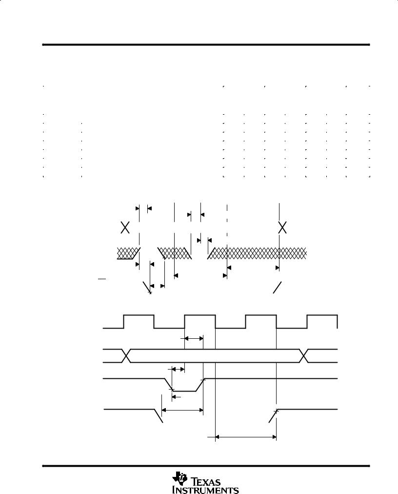
MEMORY AND PARALLEL I/O INTERFACE WRITE (CONTINUED)
A0 ± A15 |
VALID |
VALID |
|
|
th(RDH-AV) |
tsu(AV-WEL) |
|
R/W |
ta(RDAV) |
th(WEH-AV) |
|
|
|
||
|
ta(RDL-RD) |
|
|
|
tsu(RD-RDH) |
ten(WEL-BUd) |
th(WEH-WDV) |
|
|
th(RDH-RD) |
|
DATA |
VALID |
VALID |
|
|
tsu(AV-RDL) |
tsu(WDV-WEH) |
|
|
|
|
|
RD |
|
|
|
|
tw(RDH) |
td(RDH-WEL) |
|
|
tw(WEL) |
td(WEH-RDL) |
|
|
tw(RDL) |
|
|
|
|
tw(WEH) |
|
|
|
|
|
WE |
|
td(CO-RD) |
|
|
|
|
|
STRB |
|
|
|
|
|
td(CO-WE) |
td(CO-ST) |
CLKOUT1
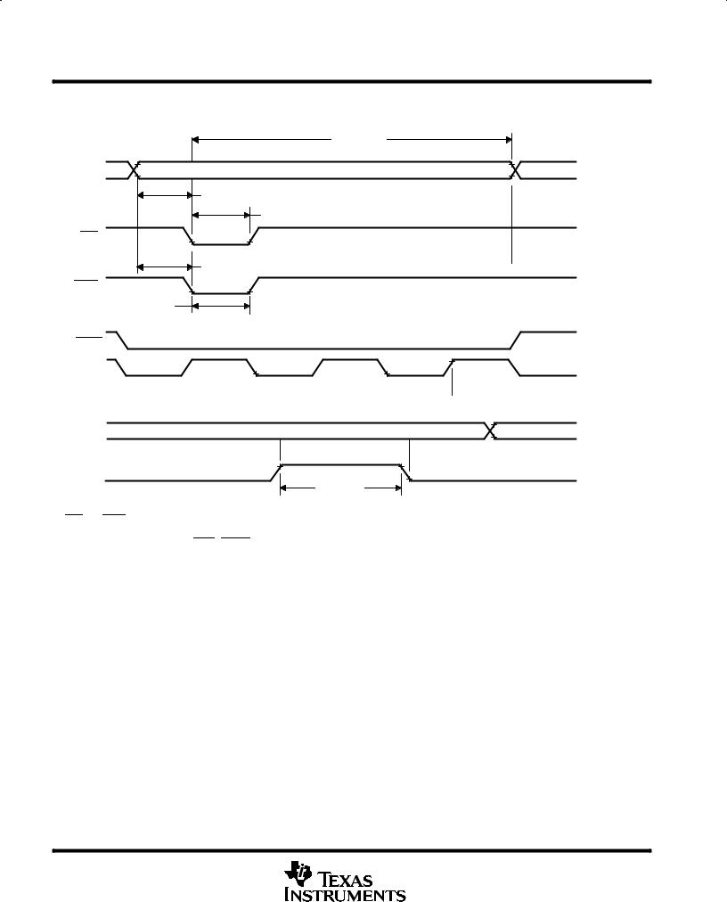
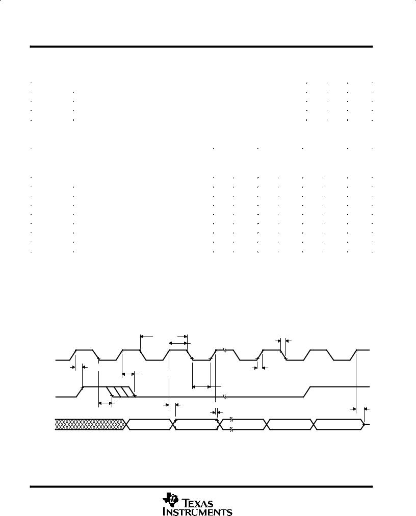
NOTES: A. All timings are for 0 wait states. However, external writes always require two cycles to prevent external bus conflicts. The diagram illustrates a one-cycle read and a two-cycle write and is not drawn to scale. All external writes immediately preceded by an external read or immediately followed by an external read require three machine cycles.
B. Refer to Appendix B of TMS320C5x User's Guide (literature number SPRU056) for logical timings of external interface.
Figure 15. Memory and Parallel I/O Interface Read and Write Timing
POST OFFICE BOX 1443 •HOUSTON, TEXAS 77251±1443 |
61 |
TMS320C5x, TMS320LC5x
DIGITAL SIGNAL PROCESSORS
SPRS030A ± APRIL 1995 ± REVISED APRIL 1996
MEMORY AND PARALLEL I/O INTERFACE WRITE (CONTINUED)
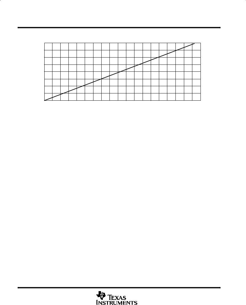
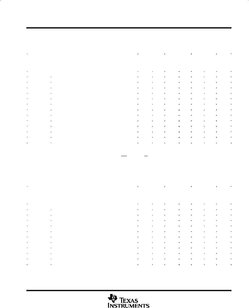
Change in Address Bus Timing ± ns
2.00
1.75
1.50
1.25
1.00
0.75
0.50
0.25
10 |
15 |
20 |
25 |
30 |
35 |
40 |
45 |
50 |
55 |
60 |
65 |
70 |
75 |
80 |
85 |
90 |
95 |
100 |
Change in Load Capacitance ± pF
Figure 16. Address Bus Timing Variation With Load Capacitance
62 |
POST OFFICE BOX 1443 •HOUSTON, TEXAS 77251±1443 |
TMS320C5x, TMS320LC5x
DIGITAL SIGNAL PROCESSORS
SPRS030A ± APRIL 1995 ± REVISED APRIL 1996
READY TIMING FOR EXTERNALLY-GENERATED WAIT STATES
timing requirements over recommended ranges of supply voltage and operating ambient-air temperature (see Note 5) (see Figure 17 and Figure 18)
|
|
|
|
|
|
|
|
|
|
|
|
|
|
|
|
|
|
|
|
|
|
|
|
|
|
|
|
|
|
|
|
|
|
|
|
|
|
|
|
|
'320C5x-40 |
|
|
|
|
|
|
|
|
|
|
||
|
|
|
|
|
|
|
|
|
|
|
|
|
|
|
|
|
|
|
|
|
|
|
|
|
|
|
|
|
|
|
|
|
|
|
|
|
|
|
|
|
'320C5x-57 |
|
'320C5x-80 |
'320C5x-100 |
|
||||||||
|
|
|
|
|
|
|
|
|
|
|
|
|
|
|
|
|
|
|
|
|
|
|
|
|
|
|
|
|
|
|
|
|
|
|
|
|
|
|
|
|
'320LC5x-40 |
|
'320LC5x-80 |
UNIT |
|||||||||
|
|
|
|
|
|
|
|
|
|
|
|
|
|
|
|
|
|
|
|
|
|
|
|
|
|
|
|
|
|
|
|
|
|
|
|
|
|
|
|
|
|
|
|||||||||||
|
|
|
|
|
|
|
|
|
|
|
|
|
|
|
|
|
|
|
|
|
|
|
|
|
|
|
|
|
|
|
|
|
|
|
|
|
|
|
|
|
'320LC5x-50 |
|
|
|
|
|
|
|
|
|
|
||
|
|
|
|
|
|
|
|
|
|
|
|
|
|
|
|
|
|
|
|
|
|
|
|
|
|
|
|
|
|
|
|
|
|
|
|
|
|
|
|
|
|
|
|
|
|
|
|
|
|
|
|
|
|
|
|
|
|
|
|
|
|
|
|
|
|
|
|
|
|
|
|
|
|
|
|
|
|
|
|
|
|
|
|
|
|
|
|
|
|
|
|
|
|
|
MIN MAX |
|
MIN MAX |
MIN MAX |
|
||||||||
|
|
|
|
|
|
|
|
|
|
|
|
|
|
|
|
|
|
|
|
|
|
|
|
|
|
|
|
|
|
|
|
|
|
|
|
|
|
|
|
|
|
|
|
|
|
|
|
|
|
|
|
|
|
tsu(RY-COH) |
Setup time, READY before CLKOUT1 rising edge |
|
|
|
10 |
|
|
7 |
|
6 |
ns |
||||||||||||||||||||||||||||||||||||||||||
tsu(RY-RDL) |
Setup time, READY before |
|
|
|
|
falling edge |
|
|
|
|
|
|
|
|
|
|
|
|
|
10 |
|
|
7 |
|
6 |
ns |
|||||||||||||||||||||||||||
RD |
|
|
|
|
|
|
|
|
|
|
|
|
|
|
|
|
|
||||||||||||||||||||||||||||||||||||
th(COH-RYH) |
Hold time, READY after CLKOUT1 rising edge |
|
|
|
0 |
|
|
0 |
|
0 |
ns |
||||||||||||||||||||||||||||||||||||||||||
|
|
|
|
|
|
|
|
|
|
|
|
|
|
|
|
|
|
|
|
|
|
|
|
|
|
|
|
|
|
|
|
|
|
|
|
|
|
|
|
|
|
|
|
|
|
|
|
|
|
|
|
||
th(RDL-RY) |
Hold time, READY after |
RD |
|
falling edge |
|
|
|
|
|
|
|
|
|
|
|
|
|
0 |
|
|
0 |
|
0 |
ns |
|||||||||||||||||||||||||||||
th(WEL-RY) |
Hold time, READY after |
|
|
|
|
|
falling edge |
|
|
|
|
|
|
|
|
|
|
|
|
|
|
H + 5 |
|
H + 4 |
H + 3 |
ns |
|||||||||||||||||||||||||||
WE |
|
|
|
|
|
|
|
|
|
|
|
|
|
|
|
|
|||||||||||||||||||||||||||||||||||||
tv(WEL-RY) |
Valid time, READY after |
|
|
|
|
falling edge |
|
|
|
|
|
|
|
|
|
|
|
|
|
|
|
H ± 15 |
|
|
|
|
|
|
|
H ± 10 |
H ± 8 |
ns |
|||||||||||||||||||||
WE |
|
|
|
|
|
|
|
|
|
|
|
|
|
|
|
|
|
|
|
|
|
|
|||||||||||||||||||||||||||||||
NOTE 5: The external READY input is sampled only after the internal software wait states are completed. |
|
|
|||||||||||||||||||||||||||||||||||||||||||||||||||
|
|
|
|
|
|
|
|
|
|
|
|
|
|
|
|
|
|
|
|
|
|
|
|
|
|
|
|
|
|
|
|
|
|
|
|
|
|
|
|
|
|
|
|
|
|
|
|
|
|
|
|
||
|
CLKOUT1 |
|
|
|
|
|
|
|
|
|
|
|
|
|
|
|
|
|
|
|
|
|
|
|
|
|
|
|
|
|
|
|
|
|
|
|
|
|
|
|
|
|
|
|
|
|
|
|
|
|
|||
|
|
|
|
|
|
|
|
|
|
|
|
|
|
|
|
|
|
|
|
|
|
|
|
|
|
|
|
|
|
|
|
|
|
|
|
|
|
|
|
|
|
|
|
|
|
|
|
|
|
|
|
||
|
tsu(RY-COH) |
|
|
|
|
|
|
|
|
|
|
|
|
|
|
|
|
|
|
|
|
|
|
|
|
|
|
tsu(RY-COH) |
|
|
|
|
|
|
|
|
|
||||||||||||||||
|
|
|
|
|
|
|
|
|
|
|
|
|
|
|
|
|
|
|
|
|
|
|
|
|
|
|
|
|
|
|
|
||||||||||||||||||||||
|
|
|
|
|
|
|
|
|
|
|
|
|
|
|
|
|
|
|
|
|
|
|
|
|
|
|
|
|
|
|
|
|
|
|
|
|
|
|
|
|
|
|
|
|
|||||||||
|
A0 ± A15 |
|
|
|
|
|
|
|
|
|
|
|
|
|
|
|
|
|
|
|
|
|
|
|
|
|
|
|
|
|
|
|
|
|
|
|
|
|
|
||||||||||||||
|
|
|
|
|
|
|
|
|
|
|
|
|
|
|
|
|
|
|
|
|
|
|
|
|
|
|
|
|
|
|
|
|
|
|
|
|
|
|
th(COH-RYH) |
|
|
|
|
|
|
|
|
|
|||||
|
|
|
|
|
|
|
|
|
|
|
|
|
|
|
|
|
|
|
|
|
|
|
|
|
|
|
|
|
|
|
|
|
|
|
|
|
|
|
|
|
|
|
|
|
|
|
|||||||
|
READY |
|
|
|
|
|
|
|
|
|
|
|
|
|
|
|
|
|
|
|
|
|
|
|
|
|
|
|
|
|
|
|
|
|
|
|
|
|
|
||||||||||||||
|
tsu(RY-RDL) |
|
|
|
|
|
|
|
|
|
|
|
|
|
|
|
|
|
|
|
Wait State |
|
|
|
|
|
Wait State |
|
|
|
|
|
|
|
|
|
|||||||||||||||||
|
|
|
|
|
|
|
|
|
|
|
|
|
|
|
|
|
|
|
|
|
|
|
|
|
|
|
|
|
|
|
|||||||||||||||||||||||
|
|
|
|
|
|
|
|
|
|
|
|
|
|
|
|
|
|
|
|
|
|
|
|
|
|
|
|
|
|
|
|
Generated |
|
|
|
|
|
|
|
|
|
||||||||||||
|
|
|
|
|
|
|
|
|
|
|
|
|
|
|
|
|
|
|
|
|
|
|
|
|
|
|
Generated |
|
|
|
|
|
by READY |
|
|
|
|
|
|
|
|
|
|||||||||||
|
|
|
|
|
|
|
|
|
|
|
|
|
|
|
|
|
|
|
|
|
|
|
|
|
|
|
|
|
|
|
|
|
|
|
|
|
|
|
|
|
|||||||||||||
|
RD |
|
|
|
|
|
|
|
|
|
|
|
|
|
|
|
|
|
|
|
|
|
|
|
|
|
|
Internally |
|
|
|
|
|
|
|
|
|
|
|
|
|
|
|
|
|
||||||||
|
|
|
|
|
|
|
|
|
|
|
|
|
|
|
|
|
|
|
|
|
|
|
|
|
|
|
|
|
|
|
|
|
|
|
|
|
|
|
|
|
|
|
|
|
|
|
|
|
|||||
|
|
|
|
|
|
|
|
|
|
|
|
|
|
|
|
|
|
|
|
|
|
|
th(RDL-RY) |
|
|
|
|
|
|
|
|
|
|
|
|
|
|
|
|
|
|
|
|
|
|
||||||||
|
|
|
|
|
|
|
|
|
|
|
|
|
|
|
|
|
|
|
|
|
|
|
|
|
|
|
|
|
|
|
|
|
|
|
|
|
|
|
|
|
|
|
|
|
|
||||||||
|
|
|
|
|
|
|
|
|
|
|
|
|
|
|
|
|
|
|
|
|
|
|
|
|
|
|
|
|
|
|
|
|
|
|
|
|
|
|
|
|
|
|
|
|
|
|
|
|
|
|
|
|
|
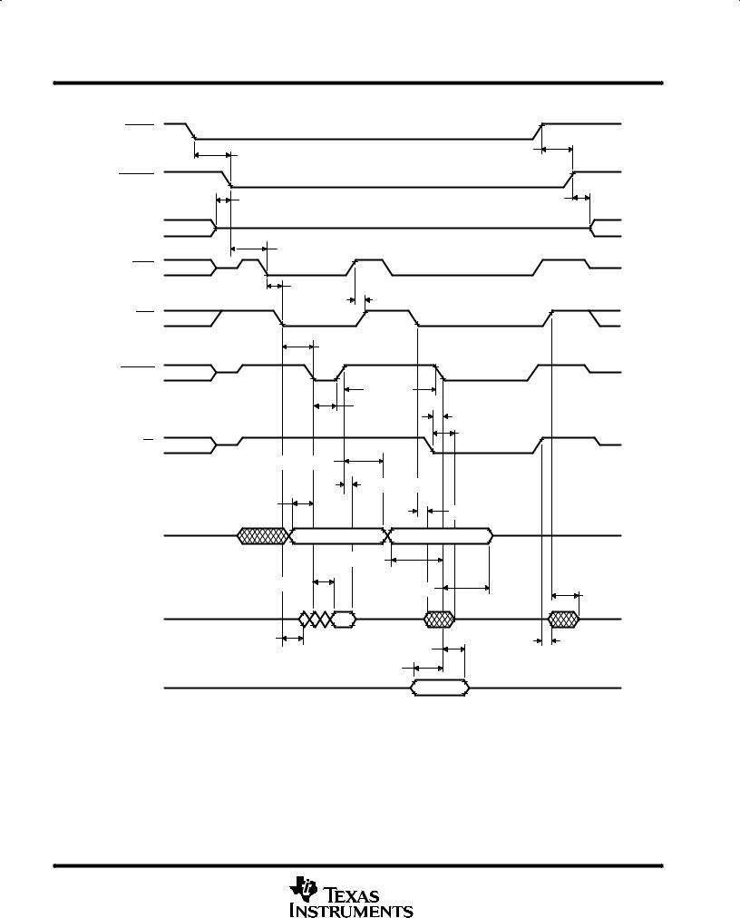
Figure 17. Ready Timing for Externally-Generated Wait States During an External Read Cycle
CLKOUT1
th(COH-RYH)
A0 ± A15
tsu(RY-COH)
READY
tv(WEL-RY) 
WE |
|
|
|
|
th(WEL-RY) |
|
|
|
|
|
|
||
|
|
|
|
|
|
|
|
|
|
|
|
|
|
Wait State Generated by READY
Figure 18. Ready Timing for Externally-Generated Wait States During an External Write Cycle
POST OFFICE BOX 1443 •HOUSTON, TEXAS 77251±1443 |
63 |
TMS320C5x, TMS320LC5x
DIGITAL SIGNAL PROCESSORS
SPRS030A ± APRIL 1995 ± REVISED APRIL 1996
RESET, INTERRUPT, AND BIO
timing requirements over recommended ranges of supply voltage and operating ambient-air temperature [H = 0.5tc(CO)] (see Figure 19)
|
|
|
|
|
|
|
|
|
|
|
|
|
|
|
|
|
|
|
|
|
|
|
|
|
|
|
|
'320C5x-40 |
'320C5x-80 |
|
||
|
|
|
|
|
|
|
|
|
|
|
|
|
|
|
|
|
|
|
|
|
|
|
|
|
|
|
|
'320C5x-57 |
|
|||
|
|
|
|
|
|
|
|
|
|
|
|
|
|
|
|
|
|
|
|
|
|
|
|
|
|
|
|
'320C5x-100 |
|
|||
|
|
|
|
|
|
|
|
|
|
|
|
|
|
|
|
|
|
|
|
|
|
|
|
|
|
|
|
'320LC5x-40 |
UNIT |
|||
|
|
|
|
|
|
|
|
|
|
|
|
|
|
|
|
|
|
|
|
|
|
|
|
|
|
|
|
'320LC5x-80 |
||||
|
|
|
|
|
|
|
|
|
|
|
|
|
|
|
|
|
|
|
|
|
|
|
|
|
|
|
|
'320LC5x-50 |
|
|||
|
|
|
|
|
|
|
|
|
|
|
|
|
|
|
|
|
|
|
|
|
|
|
|
|
|
|
|
|
|
|
||
|
|
|
|
|
|
|
|
|
|
|
|
|
|
|
|
|
|
|
|
|
|
|
|
|
|
|
|
|
|
|
|
|
|
|
|
|
|
|
|
|
|
|
|
|
|
|
|
|
|
|
|
|
|
|
|
|
|
|
|
|
MIN |
MAX |
MIN |
MAX |
|
|
|
|
|
|
|
|
|
|
|
|
|
|
|
|
|
|
|
|
|
|
|
|
|
|
|
|
|
|
|
|
|
|
|
t |
Setup time, |
|
|
|
|
|
|
|
|
|
|
|
|
|
|
|
|
|
|
|
|
|
|
15 |
|
10 |
|
ns |
|||
|
INT1±INT4, NMI before CLKOUT1 low ² |
|
|
|||||||||||||||||||||||||||||
|
su(IN-COL) |
|
|
|
|
|
|
|
|
|
|
|
|
|
|
|
|
|
|
|
|
|
|
|
|
|
|
|
|
|
|
|
|
tsu(RS-COL) |
Setup time, |
|
|
|
|
|
|
before CLKOUT1 low |
15 |
2H ± 5³ |
10 |
2H ± 5³ |
ns |
||||||||||||||||||
|
RS |
|
|
|
||||||||||||||||||||||||||||
|
|
|
|
|
|
|
|
|
|
|
|
|
|
|
|
|
|
|
|
|
|
|
|
|
|
|
||||||
|
tsu(RS-CIL) |
Setup time, |
RS |
|
|
|
before X2/CLKIN low |
10 |
|
7 |
|
ns |
||||||||||||||||||||
|
tsu(BI-COL) |
Setup time, |
|
|
|
|
|
|
|
|
|
before CLKOUT1 low |
15 |
|
10 |
|
ns |
|||||||||||||||
|
BIO |
|
|
|
||||||||||||||||||||||||||||
|
t |
Hold time, |
|
|
|
|
|
|
|
|
|
|
|
|
|
|
|
|
|
|
|
|
|
|
|
|
|
0 |
|
0 |
|
ns |
|
INT1±INT4, NMI after CLKOUT1 low ² |
|
|
|||||||||||||||||||||||||||||
|
h(COL-IN) |
|
|
|
|
|
|
|
|
|
|
|
|
|
|
|
|
|
|
|
|
|
|
|
|
|
|
|
|
|
|
|
|
th(COL-BI) |
Hold time, |
|
|
|
|
|
after CLKOUT1 low |
0 |
|
0 |
|
ns |
|||||||||||||||||||
|
BIO |
|
|
|
||||||||||||||||||||||||||||
|
t |
Pulse duration, |
|
|
|
|
|
|
|
|
|
|
|
|
|
|
|
|
4H + 15§ |
|
4H + 10§ |
|
ns |
|||||||||
|
INT1±INT4, NMI low, synchronous |
|
|
|||||||||||||||||||||||||||||
|
w(INL)SYN |
|
|
|
|
|
|
|
|
|
|
|
|
|
|
|
|
|
|
|
|
|
|
|
|
|
|
|
|
|
|
|
|
|
|
|
|
|
|
|
|
|
|
|
|
|
|
|
2H + 15§ |
|
2H + 10§ |
|
|
||||||||||||
|
tw(INH)SYN |
Pulse duration, |
INT1±INT4, NMI high, synchronous |
|
|
ns |
||||||||||||||||||||||||||
|
tw(INL)ASY |
Pulse duration, |
|
|
|
|
|
|
|
|
|
|
|
|
|
|
|
|
|
|
6H + 15§ |
|
6H + 10§ |
|
ns |
|||||||
|
INT1±INT4, NMI low, asynchronous ³ |
|
|
|||||||||||||||||||||||||||||
|
tw(INH)ASY |
Pulse duration, |
|
|
|
|
|
|
|
|
|
|
|
|
|
|
|
|
|
|
4H + 15§ |
|
4H + 10§ |
|
ns |
|||||||
|
INT1±INT4, NMI high, asynchronous ³ |
|
|
|||||||||||||||||||||||||||||
|
tw(RSL) |
Pulse duration, |
|
|
|
|
|
low |
12H |
|
12H |
|
ns |
|||||||||||||||||||
|
RS |
|
|
|||||||||||||||||||||||||||||
|
tw(BIL)SYN |
Pulse duration, |
|
|
|
|
|
|
|
low, synchronous |
15 |
|
10 |
|
ns |
|||||||||||||||||
|
BIO |
|
|
|
||||||||||||||||||||||||||||
|
t |
Pulse duration, |
|
|
|
|
|
|
|
low, asynchronous ³ |
H + 15 |
|
H + 10 |
|
ns |
|||||||||||||||||
|
BIO |
|
|
|||||||||||||||||||||||||||||
|
w(BIL)ASY |
|
|
|
|
|
|
|
|
|
|
|
|
|
|
|
|
|
|
|
|
|
|
|
|
|
|
|
|
|
|
|
|
td(RSH) |
Delay time, |
|
|
|
|
high to reset vector fetch |
34H |
|
34H |
|
ns |
||||||||||||||||||||
|
RS |
|
|
|||||||||||||||||||||||||||||
² |
These parameters must be met to use the synchronous timings. Both reset and the interrupts can operate asynchronously. The pulse durations |
|||||||||||||||||||||||||||||||
³ |
require an extra half-cycle to ensure internal synchronization. |
|
|
|
|
|
||||||||||||||||||||||||||
Values derived from characterization data and not tested |
|
|
|
|
|
|||||||||||||||||||||||||||
§ If in IDLE2, add 4H to these timings.
X2/CLKIN
tsu(RS-CIL) |
td(RSH) |
RS |
tw(RSL) |
|
tsu(BI-COL) |
tsu(RS-COL) |
CLKOUT1 

 tw(BIL)SYN
BIO
th(COL-BI)
A0 ± A15
INT4 ± INT1
tsu(IN-COL) |
tsu(IN-COL) |
th(COL-IN) |
|
tw(INL)SYN |
|||
tw(INH)SYN |
|||
|
|
||
Figure 19. Reset, Interrupt, and BIO Timings
64 |
POST OFFICE BOX 1443 •HOUSTON, TEXAS 77251±1443 |
TMS320C5x, TMS320LC5x
DIGITAL SIGNAL PROCESSORS
SPRS030A ± APRIL 1995 ± REVISED APRIL 1996
INSTRUCTION ACQUISITION (IAQ), INTERRUPT ACKNOWLEDGE (IACK),
EXTERNAL FLAG (XF), AND TOUT (SEE NOTE 6)
switching characteristics over recommended operating conditions [H = 0.5tc(CO)] (see Figure 20)
|
|
|
|
|
|
|
|
|
|
|
|
'320C5x-40 |
'320C5x-80 |
|
||
|
|
|
|
|
|
|
|
|
|
|
|
'320C5x-57 |
|
|||
|
|
|
|
|
|
|
|
|
|
|
|
'320C5x-100 |
|
|||
|
|
|
PARAMETER |
'320LC5x-40 |
UNIT |
|||||||||||
|
|
|
'320LC5x-80 |
|||||||||||||
|
|
|
|
|
|
|
|
|
|
|
|
'320LC5x-50 |
|
|||
|
|
|
|
|
|
|
|
|
|
|
|
|
|
|
||
|
|
|
|
|
|
|
|
|
|
|
|
|
|
|
|
|
|
|
|
|
|
|
|
|
|
|
|
|
MIN |
MAX |
MIN |
MAX |
|
|
|
|
|
|
|
|
|
|
|
|
|
|
|
|
|
|
tsu(AV-IQL) |
Setup time, address valid before |
|
|
|
low ² |
H ± 12³ |
|
H ± 9³ |
|
ns |
||||||
IAQ |
|
|
||||||||||||||
th(IQL-AV) |
Hold time, address valid after |
|
|
|
low |
H ± 10³ |
|
H ± 7³ |
|
ns |
||||||
IAQ |
|
|
||||||||||||||
|
|
|
|
|
|
H ± 10³ |
|
H ± 7³ |
|
|
||||||
t |
Pulse duration, |
IAQ |
low |
|
|
ns |
||||||||||
w(IQL) |
|
|
|
|
|
|
|
|
|
|
|
|
|
|
|
|
td(CO-TU) |
Delay time, CLKOUT1 falling edge to TOUT |
± 6 |
6 |
± 6 |
6 |
ns |
||||||||||
t |
Setup time, address valid before |
|
|
|
|
|
low § |
H ± 12³ |
|
H ± 9³ |
|
ns |
||||
IACK |
|
|
||||||||||||||
su(AV-IKL) |
|
|
|
|
|
|
|
|
|
|
|
|
|
|
|
|
th(IKL-AV) |
Hold time, address valid after |
|
|
|
|
low |
H ± 10³ |
|
H ± 7³ |
|
ns |
|||||
IACK |
|
|
||||||||||||||
t |
Pulse duration, |
|
|
low |
H ± 10³ |
|
H ± 7³ |
|
ns |
|||||||
IACK |
|
|
||||||||||||||
w(IKL) |
|
|
|
|
|
|
|
|
|
|
|
|
|
|
|
|
tw(TUH) |
Pulse duration, TOUT high |
2H ± 12 |
|
2H ± 9 |
|
ns |
||||||||||
td(CO-XFV) |
Delay time, XF valid after CLKOUT1 |
0 |
12 |
0 |
9 |
ns |
||||||||||
²IAQ goes low during an instruction acquisition. It goes low only on the first cycle of the read when wait states are used. The falling edge should be used to latch the valid address. The AVIS bit in the PMST register must be set to zero for the address to be valid when the instruction being addressed resides in on-chip memory.
³Valid only if the external address reflects the current instruction activity (that is, code is executing on chip with no external bus cycles and AVIS is on or code is executing off chip)
§IACK goes low during the fetch of the first word of the interrupt vector. It goes low only on the first cycle of the read when wait states are used. Address pins A1 ± A4 can be decoded at the falling edge to identify the interrupt being acknowledged. The AVIS bit in the PMST register must be set to zero for the address to be valid when the vectors reside in on-chip memory.
NOTE 6: IAQ pin is not present on 100-pin packages.
IACK pin is not present on 100-pin and 128-pin packages.
POST OFFICE BOX 1443 •HOUSTON, TEXAS 77251±1443 |
65 |
TMS320C5x, TMS320LC5x
DIGITAL SIGNAL PROCESSORS
SPRS030A ± APRIL 1995 ± REVISED APRIL 1996
INSTRUCTION ACQUISITION (IAQ), INTERRUPT ACKNOWLEDGE (IACK), EXTERNAL FLAG (XF), AND TOUT (SEE NOTE 6) (CONTINUED)
th(IQL-AV)
ADDRESS
tsu(AV-IQL)
tw(IQL)
IAQ²
 th(IKL-AV)
  tsu(AV-IKL)
IACK²
tw(IKL)
STRB
CLKOUT1
 td(CO-TU)

 td(CO-XFV) td(CO-TU)
XF
TOUT
tw(TUH)
² IAQ and IACK are not affected by wait states.
Figure 20. IAQ, IACK, and XF Timings Example With Two External Wait States
66 |
POST OFFICE BOX 1443 •HOUSTON, TEXAS 77251±1443 |
TMS320C5x, TMS320LC5x
DIGITAL SIGNAL PROCESSORS
SPRS030A ± APRIL 1995 ± REVISED APRIL 1996
EXTERNAL DMA
switching characteristics over recommended operating conditions [H = 0.5tc(CO)] (see Note 7) (see Figure 21)
|
|
|
|
|
|
|
|
|
|
|
|
|
|
|
|
|
|
|
|
|
|
|
|
|
|
|
|
|
|
|
'320C5x-40 |
|
|
|
|
|
|
|
|
|
|
|
|
|
|
|
|
|
|
|
|
|
|
|
|
|
|
|
|
|
|
|
|
|
|
|
|
|
'320C5x-57 |
'320C5x-80 |
'320C5x-100 |
|
|||
|
|
|
|
|
|
|
PARAMETER |
'320LC5x-40 |
'320LC5x-80 |
UNIT |
|||||||||||||||||||||||||||
|
|
|
|
|
|
|
|
|
|||||||||||||||||||||||||||||
|
|
|
|
|
|
|
|
|
|
|
|
|
|
|
|
|
|
|
|
|
|
|
|
|
|
|
|
|
|
|
'320LC5x-50 |
|
|
|
|
|
|
|
|
|
|
|
|
|
|
|
|
|
|
|
|
|
|
|
|
|
|
|
|
|
|
|
|
|
|
|
|
|
|
|
|
|
|
|
|
|
|
|
|
|
|
|
|
|
|
|
|
|
|
|
|
|
|
|
|
|
|
|
|
|
|
|
|
|
|
|
MIN |
MAX |
MIN |
MAX |
MIN |
MAX |
|
|
|
|
|
|
|
|
|
|
|
|
|
|
|
|
|
|
|
|
|
|
|
|
|
|
|
|
|
|
|
|
|
|
|
|
|
||
td(HOL-HAL) |
Delay time, |
|
|
|
|
|
|
|
low to |
|
|
|
|
|
|
|
|
|
low |
4H |
² |
4H |
² |
4H |
² |
ns |
|||||||||||
HOLD |
HOLDA |
||||||||||||||||||||||||||||||||||||
td(HOH-HAH) |
Delay time, |
|
|
|
|
|
|
|
high before |
|
|
|
|
|
|
high |
2H |
|
2H |
|
2H |
|
ns |
||||||||||||||
HOLD |
HOLDA |
|
|
|
|
||||||||||||||||||||||||||||||||
t |
|
|
Address high-impedance before |
|
|
|
low³ |
H ± 15§ |
|
H ± 10§ |
|
H ± 8§ |
|
ns |
|||||||||||||||||||||||
h(AZ-HAL) |
HOLDA |
|
|
|
|||||||||||||||||||||||||||||||||
|
|
|
|
|
|
|
|
|
|
|
|
|
|
|
|
|
|
|
|
|
|
|
|
|
|
|
|
|
|
|
|
|
|
|
|
||
ten(HAH-Ad) |
Enable time, |
|
|
|
|
|
|
|
high to address driven |
H ± 5§ |
|
H ± 4§ |
|
H ± 3§ |
|
ns |
|||||||||||||||||||||
HOLDA |
|
|
|
||||||||||||||||||||||||||||||||||
td(XBL-IQL) |
Delay time, |
|
|
|
|
|
low to |
|
|
|
|
low |
4H§ |
6H§ |
4H§ |
6H§ |
4H§ |
6H§ |
ns |
||||||||||||||||||
XBR |
|
IAQ |
|
||||||||||||||||||||||||||||||||||
td(XBH-IQH) |
Delay time, |
|
|
|
|
|
|
high to |
|
|
|
|
high |
2H§ |
4H§ |
2H§ |
4H§ |
2H§ |
4H§ |
ns |
|||||||||||||||||
XBR |
|
IAQ |
|||||||||||||||||||||||||||||||||||
td(XSL-RDV) |
Delay time, read data valid after |
|
|
|
|
|
low |
|
40 |
|
29 |
|
25 |
ns |
|||||||||||||||||||||||
XSTRB |
|
|
|
||||||||||||||||||||||||||||||||||
|
|
|
|
|
|
|
|
|
|
|
|
|
|
|
|
|
|
||||||||||||||||||||
th(XSH-RD) |
Hold time, read data valid after |
XSTRB |
high |
0 |
|
0 |
|
0 |
|
ns |
|||||||||||||||||||||||||||
t |
|
|
Enable time, |
|
|
|
|
|
low to read data driven¶ |
0§ |
2H§ |
0§ |
2H§ |
0§ |
2H§ |
ns |
|||||||||||||||||||||
en(IQL-RDd) |
IAQ |
||||||||||||||||||||||||||||||||||||
|
|
|
|
|
|
|
|
|
|
|
|
|
|
|
|
|
|
|
|
|
|
|
|
|
|
|
|
|
|
|
|
|
|
|
|
||
th(XRL-DZ) |
Hold time, XR / |
|
|
|
low to data high impedance |
0§ |
15§ |
0§ |
10§ |
0§ |
8 |
ns |
|||||||||||||||||||||||||
W |
|||||||||||||||||||||||||||||||||||||
t |
|
|
Hold time, |
|
|
|
|
high to data high impedance |
|
H§ |
|
H§ |
|
H§ |
ns |
||||||||||||||||||||||
h(IQH-DZ) |
IAQ |
|
|
|
|||||||||||||||||||||||||||||||||
|
|
|
|
|
|
|
|
|
|
|
|
|
|
|
|
|
|
|
|
|
|
|
|
|
|
|
|
|
|
|
|
|
|
|
|
||
ten(D-XRH) |
Enable time, data from XR / |
|
|
going high |
|
4§ |
|
3§ |
|
2§ |
ns |
||||||||||||||||||||||||||
W |
|
|
|
||||||||||||||||||||||||||||||||||
² |
|
|
|
|
|
|
|
||||||||||||||||||||||||||||||
HOLD |
is not acknowledged until current external access request is complete. |
|
|
|
|
|
|
||||||||||||||||||||||||||||||
³ |
This parameter includes all memory control lines. |
|
|
|
|
|
|
|
|||||||||||||||||||||||||||||
§ Values derived from characterization data and not tested |
|
|
|
|
|
|
|
||||||||||||||||||||||||||||||
¶This parameter refers to the delay between the time the condition (IAQ = 0 and XR / W = 1) is satisfied and the time that the 'C5x data lines become valid.
NOTE 7: X preceding a name refers to external drive of the signal.
timing requirements over recommended ranges of supply voltage and operating ambient-air temperature (see Note 7) (see Figure 21)
|
|
|
|
|
|
|
|
|
|
|
|
|
|
|
|
|
|
|
|
|
|
|
|
|
|
|
'320C5x-40 |
|
|
|
|
|
|
|
|
|
|
|
|
|
|
|
|
|
|
|
|
|
|
|
|
|
|
|
|
|
|
|
'320C5x-57 |
'320C5x-80 |
'320C5x-100 |
|
|
|
|
|
|
|
|
|
|
|
|
|
|
|
|
|
|
|
|
|
|
|
|
|
|
|
|
|
'320LC5x-40 |
'320LC5x-80 |
UNIT |
||
|
|
|
|
|
|
|
|
|
|
|
|
|
|
|
|
|
|
|
|
|
|
|
|
|
|
|
|
|
|||
|
|
|
|
|
|
|
|
|
|
|
|
|
|
|
|
|
|
|
|
|
|
|
|
|
|
|
'320LC5x-50 |
|
|
|
|
|
|
|
|
|
|
|
|
|
|
|
|
|
|
|
|
|
|
|
|
|
|
|
|
|
|
|
|
|
|
|
|
|
|
|
|
|
|
|
|
|
|
|
|
|
|
|
|
|
|
|
|
|
|
|
|
|
|
|
MIN MAX |
MIN MAX |
MIN |
MAX |
|
|
|
|
|
|
|
|
|
|
|
|
|
|
|
|
|
|
|
|
|
|
|
|
|
|
|
|
|
|
|
|
|
td(HAL-XBL) |
Delay time, |
|
|
|
|
|
|
low to |
|
|
|
|
|
|
low# |
0§ |
0§ |
0§ |
|
ns |
|||||||||||
HOLDA |
XBR |
|
|||||||||||||||||||||||||||||
td(IQL-XSL) |
Delay time, |
|
|
|
|
low to |
|
|
|
|
|
|
|
low# |
0§ |
0§ |
0§ |
|
ns |
||||||||||||
IAQ |
XSTRB |
|
|||||||||||||||||||||||||||||
tsu(AV-XSL) |
Setup time, Xaddress valid before |
|
|
|
|
|
|
low |
15 |
12 |
10 |
|
ns |
||||||||||||||||||
XSTRB |
|
||||||||||||||||||||||||||||||
|
|
|
|
|
|
|
|
|
|
|
|
|
|
|
|
|
|
|
|
|
|||||||||||
tsu(DV-XSL) |
Setup time, Xdata valid before |
XSTRB |
|
low |
15 |
12 |
10 |
|
ns |
||||||||||||||||||||||
th(XSL-D) |
Hold time, Xdata hold after |
|
|
|
|
|
|
|
low |
15 |
12 |
10 |
|
ns |
|||||||||||||||||
XSTRB |
|
||||||||||||||||||||||||||||||
th(XSL-WA) |
Hold time, write Xaddress hold after |
|
|
|
|
|
low |
15 |
12 |
10 |
|
ns |
|||||||||||||||||||
XSTRB |
|
||||||||||||||||||||||||||||||
tw(XSL) |
Pulse duration, |
|
|
|
|
|
|
low |
45 |
40 |
35 |
|
ns |
||||||||||||||||||
XSTRB |
|
|
|||||||||||||||||||||||||||||
tw(XSH) |
Pulse duration, |
|
|
|
|
|
|
|
high |
45 |
40 |
35 |
|
ns |
|||||||||||||||||
XSTRB |
|
||||||||||||||||||||||||||||||
tsu(RW-XSL) |
Setup time, R / |
|
|
|
|
valid before |
|
|
|
|
|
|
|
|
low |
20 |
20 |
18 |
|
ns |
|||||||||||
W |
XSTRB |
|
|||||||||||||||||||||||||||||
th(XSH-RA) |
Hold time, read Xaddress after |
|
|
|
|
|
|
|
high |
0 |
0 |
0 |
|
ns |
|||||||||||||||||
XSTRB |
|
||||||||||||||||||||||||||||||
§ Values derived from characterization data and not tested
#XBR, XR / W, and XSTRB lines must be pulled up with a 10-kΩ resistor to be certain that they are in an inactive high state during the transition period between the 'C5x driving them and the external circuit driving them.
NOTE 7: X preceding a name refers to external drive of the signal.
POST OFFICE BOX 1443 •HOUSTON, TEXAS 77251±1443 |
67 |
TMS320C5x, TMS320LC5x
DIGITAL SIGNAL PROCESSORS
SPRS030A ± APRIL 1995 ± REVISED APRIL 1996
EXTERNAL DMA (CONTINUED)
HOLD |
|
|
|
|
td(HOL-HAL) |
|
td(HOH-HAH) |
|
|
|
|
HOLDA |
|
|
|
ADDRESS |
th(AZ-HAL) |
|
ten(HAH-Ad) |
BUS/ |
|
|
|
CONTROL |
|
|
|
SIGNALS |
td(HAL-XBL) |
|
|
|
|
||
XBR |
|
|
|
|
td(XBL-IQL) |
|
|
|
|
td(XBH-IQH) |
|
IAQ |
|
|
|
|
|
td(IQL-XSL) |
|
XSTRB |
|
|
|
|
|
tw(XSH) |
|
|
|
tw(XSL) |
tsu(RW-XSL) |
|
|
|
|
XR/W |
|
|
th(XRL-DZ) |
|
|
|
|
|
th(XSH-RA) |
|
|
|
|
th(XSH-RD) |
|
|
tsu(AV-XSL) |
|
ten(IQL-RDd) |
|
|
|
|
XADDRESS |
|
|
|
|
|
tsu(AV-XSL) |
|
|
td(XSL-RDV) |
th(XSL-WA) |
th(IQH-DZ) |
|
|
||
|
|
|
|
DATA(RD) |
|
|
|
|
ten(IQL-RDd) |
th(XSL-D) |
ten(D-XRH) |
|
|
|
|
|
|
tsu(DV-XSL) |
|
XDATA(WR) |
|
|
|
Figure 21. External DMA Timing
68 |
POST OFFICE BOX 1443 •HOUSTON, TEXAS 77251±1443 |
TMS320C5x, TMS320LC5x
DIGITAL SIGNAL PROCESSORS
SPRS030A ± APRIL 1995 ± REVISED APRIL 1996
SERIAL-PORT RECEIVE TIMING
timing requirements over recommended ranges of supply voltage and operating ambient-air temperature [H = 0.5tc(CO)] (see Figure 22)
|
|
'320C5x-40 |
|
|
|
|
|
|
|
|
'320C5x-57 |
'320C5x-80 |
'320C5x-100 |
|
|||
|
|
'320LC5x-40 |
'320LC5x-80 |
UNIT |
||||
|
|
|
|
|||||
|
|
'320LC5x-50 |
|
|
|
|
|
|
|
|
|
|
|
|
|
|
|
|
|
MIN |
MAX |
MIN |
MAX |
MIN |
MAX |
|
|
|
|
|
|
|
|
|
|
tc(SCK) |
Cycle time, serial-port clock |
5.2H² |
³ |
5.2H² |
³ |
5.2H² |
³ |
ns |
tf(SCK) |
Fall time, serial-port clock |
|
8§ |
|
6§ |
|
6§ |
ns |
t |
Rise time, serial-port clock |
|
8§ |
|
6§ |
|
6§ |
ns |
r(SCK) |
|
|
|
|
|
|
|
|
tw(SCK) |
Pulse duration, serial-port clock low / high |
2.1H² |
|
2.1H² |
|
2.1H² |
|
ns |
tsu(FS-CK) |
Setup time, FSR before CLKR falling edge |
10 |
|
7 |
|
6 |
|
ns |
tsu(DR-CK) |
Setup time, DR before CLKR falling edge |
10 |
|
7 |
|
6 |
|
ns |
th(CK-FS) |
Hold time, FSR after CLKR falling edge |
10 |
|
7 |
|
6 |
|
ns |
th(CK-DR) |
Hold time, DR valid after CLKR falling edge |
10 |
|
7 |
|
6 |
|
ns |
² Values ensured by design but not tested
³The serial-port design is fully static and, therefore, can operate with tc(SCK) approaching ∞ . It is characterized approaching an input frequency of 0 Hz but tested at a much higher frequency to minimize test time.
§ Values derived from characterization data and not tested
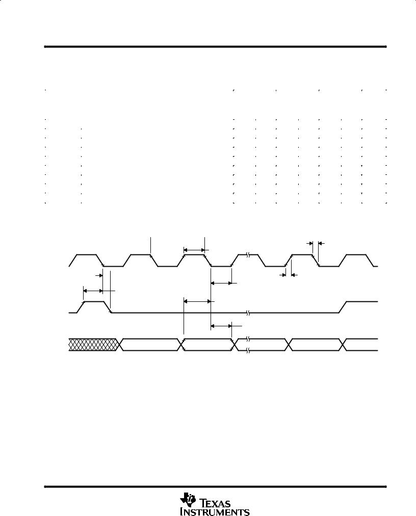
 tc(SCK)
tw(SCK)
CLKR
 th(CK-FS)
tw(SCK)
tsu(FS-CK)
tsu(DR-CK)
FSR
th(CK-DR)
DR
Bit
1 |
2 |
tf(SCK)
tr(SCK)
7/15 |
8/16 |
Figure 22. Serial-Port Receive Timing
POST OFFICE BOX 1443 •HOUSTON, TEXAS 77251±1443 |
69 |
TMS320C5x, TMS320LC5x
DIGITAL SIGNAL PROCESSORS
SPRS030A ± APRIL 1995 ± REVISED APRIL 1996
SERIAL-PORT TRANSMIT TIMING, EXTERNAL CLOCKS, AND EXTERNAL FRAMES
switching characteristics over recommended operating conditions (see Note 8) (see Figure 23)
|
PARAMETER |
MIN |
MAX |
UNIT |
|
|
|
|
|
td(CXH-DXV) |
Delay time, DX valid after CLKX high |
|
25 |
ns |
tdis(CXH-DX) |
Disable time, DX invalid after CLKX high |
|
40² |
ns |
th(CXH-DXV) |
Hold time, DX valid after CLKX high |
± 5 |
|
ns |
timing requirements over recommended ranges of supply voltage and operating ambient-air temperature [H = 0.5tc(CO)] (see Note 8) (see Figure 23)
|
|
'320C5x-40 |
|
|
|
|
|
|
|
|
'320C5x-57 |
'320C5x-80 |
'320C5x-100 |
|
|||
|
|
'320LC5x-40 |
'320LC5x-80 |
UNIT |
||||
|
|
|
|
|||||
|
|
'320LC5x-50 |
|
|
|
|
|
|
|
|
|
|
|
|
|
|
|
|
|
MIN |
MAX |
MIN |
MAX |
MIN |
MAX |
|
|
|
|
|
|
|
|
|
|
tc(SCK) |
Cycle time, serial-port clock |
5.2H³ |
§ |
5.2H³ |
§ |
5.2H³ |
§ |
ns |
tf(SCK) |
Fall time, serial-port clock |
|
8² |
|
6² |
|
6² |
ns |
tr(SCK) |
Rise time, serial-port clock |
|
8² |
|
6² |
|
6² |
ns |
t |
Pulse duration, serial-port clock low/high |
2.1H³ |
|
2.1H³ |
|
2.1H³ |
|
ns |
w(SCK) |
|
|
|
|
|
|
|
|
td(CXH-FXH) |
Delay time, FSX high after CLKX high |
|
2H ± 8 |
|
2H ± 8 |
|
2H ± 5 |
ns |
th(CXL-FXL) |
Hold time, FSX low after CLKX low |
10 |
|
7 |
|
6 |
|
ns |
th(CXH-FXL) |
Hold time, FSX low after CLKX high |
|
2H ± 8¶ |
|
2H ± 8¶ |
|
2H ± 5¶ |
ns |
² Values derived from characterization data and not tested ³ Values ensured by design but not tested
§The serial-port design is fully static and, therefore, can operate with tc(SCK) approaching ∞ . It is characterized approaching an input frequency of 0 Hz but tested at a much higher frequency to minimize test time.
¶ If the FSX pulse does not meet this specification, the first bit of serial data is driven on the DX pin until the falling edge of FSX. After the falling
edgeofFSX,dataisshiftedoutontheDXpin.Thetransmitbufferemptyinterruptisgeneratedwhentheth(CXL-FXL) and th(CXH-FXL)specification is met.
NOTE 8:
CLKX
FSX
DX
BIt
tc(SCK) |
tw(SCK) |
tf(SCK) |
|
|
|
||
td(CXH-FXH) |
|
tr(SCK) |
|
th(CXH-FXL) |
|
|
|
|
|
tw(SCK) |
|
th(CXL-FXL) |
td(CXH-DXV) |
th(CXH-DXV) |
tdis(CXH-DX) |
|
|
||
|
|
|
|
1 |
2 |
7/15 |
8/16 |
Figure 23. Serial-Port Transmit Timing of External Clocks and External Frames
70 |
POST OFFICE BOX 1443 •HOUSTON, TEXAS 77251±1443 |