

|
|
TMS320C30 |
||
|
|
DIGITAL SIGNAL PROCESSOR |
||
|
|
SPRS032A ± APRIL 1996 ± REVISED JUNE 1997 |
||
|
|
|
|
|
D High-Performance Floating-Point Digital |
D |
Two 32-Bit External Ports |
||
Signal Processor (DSP) |
D |
24and 13-Bit Addresses |
||
± TMS320C30-50 (5 V) |
||||
D 0.7-µm Enhanced Performance Implanted |
||||
40-ns Instruction Cycle Time |
||||
|
CMOS (EPIC ) Technology |
|||
275 MOPS, 50 MFLOPS, 25 MIPS |
|
|||
D 208-Pin Plastic Quad Flat Package |
||||
± TMS320C30-40 (5 V) |
||||
|
(PPM Suffix) |
|||
50-ns Instruction Cycle Time |
|
|||
|
|
|
||
220 MOPS, 40 MFLOPS, 20 MIPS |
D |
181-Pin Grid Array Ceramic Package |
||
± TMS320C30-33 (5 V) |
|
(GEL Suffix) |
||
60-ns Instruction Cycle Time |
D |
Eight Extended-Precision Registers |
||
183.3 MOPS, 33.3 MFLOPS, 16.7 MIPS |
D Two Address Generators With Eight |
|||
|
||||
± TMS320C30-27 (5 V)
74-ns Instruction Cycle Time
Auxiliary Registers and Two Auxiliary
148.5 MOPS, 27 MFLOPS, 13.5 MIPS
Register Arithmetic Units (ARAUs)
D Twoand Three-Operand Instructions
D 32-Bit High-Performance CPU
D 16- /32-Bit Integer and 32- /40-Bit
D Parallel Arithmetic and Logic Unit (ALU)
Floating-Point Operations
and Multiplier Execution in a Single Cycle
D32-Bit Instruction Word, 24-Bit Addresses
DTwo 1K × 32-Bit Single-Cycle Dual-Access
On-Chip RAM Blocks
DOne 4K × 32-Bit Single-Cycle Dual-Access
On-Chip ROM Block
DOn-Chip Memory-Mapped Peripherals:
±Two Serial Ports
±Two 32-Bit Timers
±One-Channel Direct Memory Access (DMA) Coprocessor for Concurrent I/O and CPU Operation
description
DBlock-Repeat Capability
DZero-Overhead Loops With Single-Cycle Branches
DConditional Calls and Returns
DInterlocked Instructions for Multiprocessing Support
DTwo Sets of Memory Strobes (STRB and MSTRB) and One I/O Strobe (IOSTRB)
DSeparate Bus-Control Registers for Each Strobe-Control Wait-State Generation
The TMS320C30 is the newest member of the TMS320C3x generation of DSPs from Texas Instruments (TI ). The TMS320C30 is a 32-bit floating-point processor manufactured in 0.7-µm triple-level-metal CMOS technology.
The TMS320C30's internal busing and special DSP instruction set have the speed and flexibility to execute up to 50 MFLOPS (million floating-point operations per second). The TMS320C30 optimizes speed by implementing functions in hardware that other processors implement through software or microcode. This hardware-intensive approach provides performance previously unavailable on a single chip.
The TMS320C30 can perform parallel multiply and ALU operations on integer or floating-point data in a single cycle. Each processor also possesses a general-purpose register file, a program cache, dedicated ARAUs, internal dual-access memories, one DMA channel supporting concurrent I/O, and a short machine-cycle time. High performance and ease of use are results of these features.
General-purpose applications are enhanced greatly by the large address space, multiprocessor interface, internally and externally generated wait states, two external interface ports, two timers, serial ports, and multiple interrupt structure. The TMS320C30 supports a wide variety of system applications from host processor to dedicated coprocessor.
Please be aware that an important notice concerning availability, standard warranty, and use in critical applications of Texas Instruments semiconductor products and disclaimers thereto appears at the end of this data sheet.
EPIC and TI are trademarks of Texas Instruments Incorporated.
PRODUCTION DATA information is current as of publication date. |
Copyright 1997, Texas Instruments Incorporated |
Products conform to specifications per the terms of Texas Instruments |
|
standard warranty. Production processing does not necessarily include |
|
testing of all parameters. |
|
POST OFFICE BOX 1443 •HOUSTON, TEXAS 77251±1443 |
1 |
TMS320C30
DIGITAL SIGNAL PROCESSOR
SPRS032A ± APRIL 1996 ± REVISED JUNE 1997
description (continued)
High-level language support is implemented easily through a register-based architecture, large address space, powerful addressing modes, flexible instruction set, and well-supported floating-point arithmetic.
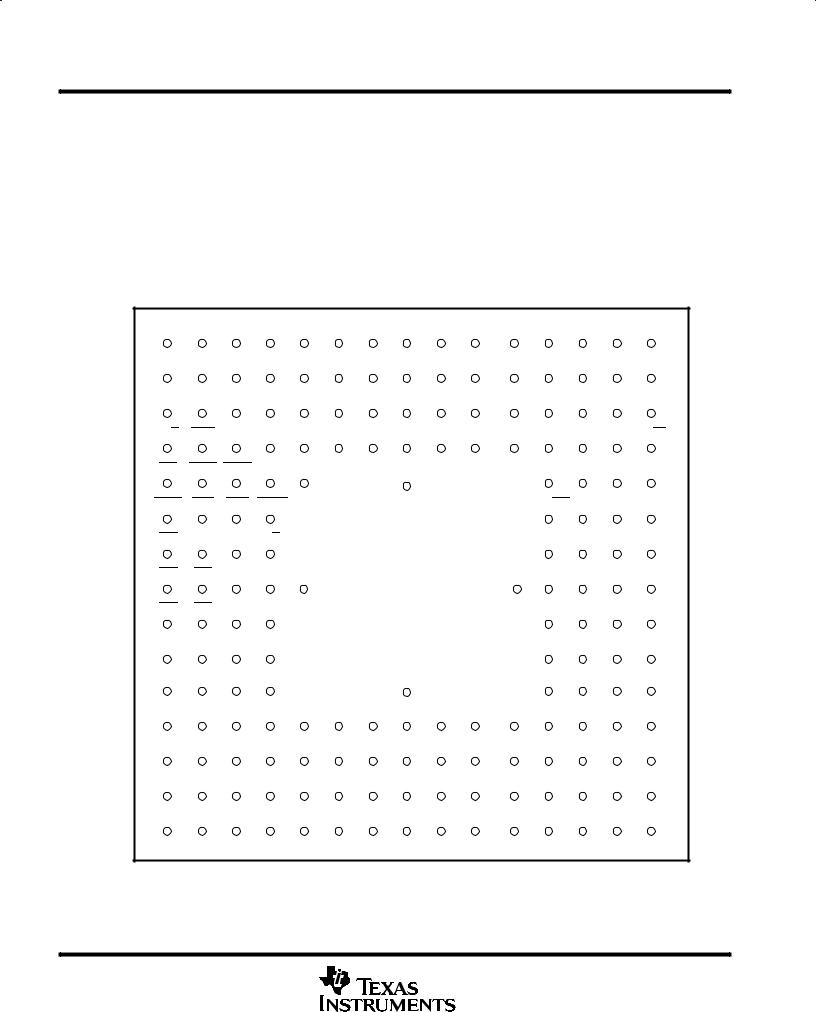
pinout and pin assignments
TMS320C30 GEL pinout and pin assignments
The TMS320C30 digital signal processor is available in a 181-pin grid array (PGA) package. The pinout of this package is shown in the following two illustrations. The pin assignments are listed in the TMS320C30 GEL pin assignments (alphabetical) table and the TMS320C30 GEL pin assignments (numerical) table.
1 |
2 |
3 |
4 |
5 |
6 |
7 |
8 |
9 |
10 |
11 |
12 |
13 |
14 |
15 |
H3 |
D2 |
D3 |
D7 |
D10 |
D13 |
D16 |
D17 |
D19 |
D22 |
D25 |
D28 |
XA0 |
XA1 |
XA5 |
A |
|
|
|
|
|
|
|
|
|
|
|
|
|
|
X2/CLKIN |
CVSS |
H1 |
D4 |
D8 |
D11 |
D15 |
D18 |
D20 |
D24 |
D27 |
D31 |
XA4 |
IVSS |
XA6 |
B |
|
|
|
|
|
|
|
|
|
|
|
|
|
|
EMU5 |
X1 |
DVSS |
D0 |
D5 |
D9 |
D14 |
VSS |
D21 |
D26 |
D30 |
XA3 |
DVSS |
XA7 |
XA10 |
C |
|
|
|
|
|
|
|
|
|
|
|
|
|
|
XR/W |
XRDY |
VBBP |
DDVDD |
D1 |
D6 |
D12 |
VDD |
D23 |
D29 |
XA2 |
ADVDD |
XA9 |
XA11 |
MC/MP |
D |
|
|
|
|
|
|
|
|
|
|
|
|
|
|
RDY |
HOLDA |
MSTRB |
VSUBS LOCATOR |
|
|
DDVDD |
|
|
|
XA8 |
XA12 |
EMU3 |
EMU1 |
|
E |
|
|
|
|
|
|
|
|
|
|
|
|
|
|
RESET |
STRB |
HOLD |
IOSTRB |
|
|
|
|
|
|
|
EMU4/SHZ EMU2 |
EMU0 |
A0 |
|
F |
|
|
|
|
|
|
|
|
|
|
|
|
|
|
IACK |
XF0 |
XF1 |
R/W |
|
|
|
|
|
|
|
A1 |
A2 |
A3 |
A4 |
G |
|
|
|
|
|
|
|
|
|
|
|
|
|
|
INT1 |
INT0 |
VSS |
VDD |
MDVDD |
|
TMS320C30 |
|
ADVDD |
VDD |
VSS |
A6 |
A5 |
||
|
|
Top View |
|
|||||||||||
H |
|
|
|
|
|
|
|
|
|
|
|
|
||
|
|
|
|
|
|
|
|
|
|
|
|
|
|
|
INT2 |
INT3 |
RSV0 |
RSV1 |
|
|
|
|
|
|
|
A11 |
A9 |
A8 |
A7 |
J |
|
|
|
|
|
|
|
|
|
|
|
|
|
|
RSV2 |
RSV3 |
RSV5 |
RSV7 |
|
|
|
|
|
|
|
A17 |
A14 |
A12 |
A10 |
K |
|
|
|
|
|
|
|
|
|
|
|
|
|
|
RSV4 |
RSV6 |
RSV9 |
CLKR1 |
|
|
|
IODVDD |
|
|
|
A22 |
A18 |
A15 |
A13 |
L |
|
|
|
|
|
|
|
|
|
|
|
|
|
|
RSV8 |
RSV10 |
FSR1 |
PDVDD |
CLKX0 |
EMU6 |
XD5 |
VDD |
XD16 |
XD22 |
XD27 |
IODVDD |
A21 |
A19 |
A16 |
M |
|
|
|
|
|
|
|
|
|
|
|
|
|
|
DR1 |
CLKX1 |
DVSS |
CLKR0 |
TCLK1 |
XD2 |
XD7 |
VSS |
XD14 |
XD19 |
XD23 |
XD28 |
DVSS |
A23 |
A20 |
N |
|
|
|
|
|
|
|
|
|
|
|
|
|
|
FSX1 |
DX1 |
FSR0 |
TCLK0 |
XD1 |
XD4 |
XD8 |
XD10 |
XD13 |
XD17 |
XD20 |
XD24 |
XD29 |
CVSS |
XD31 |
P |
|
|
|
|
|
|
|
|
|
|
|
|
|
|
DR0 |
FSX0 |
DX0 |
XD0 |
XD3 |
XD6 |
XD9 |
XD11 |
XD12 |
XD15 |
XD18 |
XD21 |
XD25 |
XD26 |
XD30 |
R
TMS320C30 GEL Pinout (Top View)
2 |
POST OFFICE BOX 1443 •HOUSTON, TEXAS 77251±1443 |

TMS320C30
DIGITAL SIGNAL PROCESSOR
SPRS032A ± APRIL 1996 ± REVISED JUNE 1997
TMS320C30 GEL pinout and pin assignments (continued)
15 |
14 |
13 |
12 |
11 |
10 |
9 |
8 |
7 |
6 |
5 |
4 |
3 |
2 |
1 |
XA5 |
XA1 |
XA0 |
D28 |
D25 |
D22 |
D19 |
D17 |
D16 |
D13 |
D10 |
D7 |
D3 |
D2 |
H3 |
XA6 |
IVSS |
XA4 |
D31 |
D27 |
D24 |
D20 |
D18 |
D15 |
D11 |
D8 |
D4 |
H1 |
CVSS |
X2/CLKIN |
XA10 |
XA7 |
DVSS |
XA3 |
D30 |
D26 |
D21 |
VSS |
D14 |
D9 |
D5 |
D0 |
DVSS |
X1 |
EMU5 |
MC/MP |
XA11 |
XA9 |
ADVDD |
XA2 |
D29 |
D23 |
VDD |
D12 |
D6 |
D1 |
DDVDD |
VBBP |
XRDY |
XR/W |
EMU1 |
EMU3 |
XA12 |
XA8 |
|
|
|
DDVDD |
|
|
LOCATOR VSUBS |
MSTRB |
HOLDA |
RDY |
|
A0 |
EMU0 |
EMU2 EMU4/SHZ |
|
|
|
|
|
|
|
IOSTRB |
HOLD |
STRB |
RESET |
|
A4 |
A3 |
A2 |
A1 |
|
|
|
|
|
|
|
R/W |
XF1 |
XF0 |
IACK |
A5 |
A6 |
VSS |
VDD |
ADVDD |
|
TMS320C30 |
|
MDVDD |
VDD |
VSS |
INT0 |
INT1 |
||
|
|
|
|
|
|
Bottom View |
|
|
|
|
|
|
||
A7 |
A8 |
A9 |
A11 |
|
|
|
|
|
|
|
RSV1 |
RSV0 |
INT3 |
INT2 |
A10 |
A12 |
A14 |
A17 |
|
|
|
|
|
|
|
RSV7 |
RSV5 |
RSV3 |
RSV2 |
A13 |
A15 |
A18 |
A22 |
|
|
|
IODVDD |
|
|
|
CLKR1 |
RSV9 |
RSV6 |
RSV4 |
A16 |
A19 |
A21 |
IODVDD |
XD27 |
XD22 |
XD16 |
VDD |
XD5 |
EMU6 |
CLKX0 |
PDVDD |
FSR1 |
RSV10 |
RSV8 |
A20 |
A23 |
DVSS |
XD28 |
XD23 |
XD19 |
XD14 |
VSS |
XD7 |
XD2 |
TCLK1 |
CLKR0 |
DVSS |
CLKX1 |
DR1 |
XD31 |
CVSS |
XD29 |
XD24 |
XD20 |
XD17 |
XD13 |
XD10 |
XD8 |
XD4 |
XD1 |
TCLK0 |
FSR0 |
DX1 |
FSX1 |
XD30 |
XD26 |
XD25 |
XD21 |
XD18 |
XD15 |
XD12 |
XD11 |
XD9 |
XD6 |
XD3 |
XD0 |
DX0 |
FSX0 |
DR0 |
A
B
C
D
E
F
G
H
J
K
L
M
N
P
R
TMS320C30 GEL Pinout (Bottom View)
POST OFFICE BOX 1443 •HOUSTON, TEXAS 77251±1443 |
3 |

TMS320C30
DIGITAL SIGNAL PROCESSOR
SPRS032A ± APRIL 1996 ± REVISED JUNE 1997
TMS320C30 GEL Pin Assignments (Alphabetical)²
PIN |
|
|
|
|
|
|
PIN |
|
|
|
|
|
|
|
|
|
PIN |
|
|
|
PIN |
|
|
|
|
|
|
PIN |
|||
NAME |
NO. |
|
|
|
NAME |
|
NO. |
|
|
NAME |
|
|
NO. |
|
|
NAME |
NO. |
|
NAME |
NO. |
|||||||||||
|
|
|
|
|
|
|
|
|
|
|
|
|
|
|
|
|
|
|
|
|
|
|
|
|
|
|
|
|
|
|
|
A0 |
F15 |
|
|
D8 |
|
|
|
|
|
B5 |
|
EMU6 |
|
|
|
M6 |
|
|
VBBP |
D3 |
|
XD15 |
R10 |
||||||||
A1 |
G12 |
|
|
D9 |
|
|
|
|
|
C6 |
|
FSR0 |
|
|
|
P3 |
|
|
VDD |
D8 |
|
XD16 |
M9 |
||||||||
A2 |
G13 |
|
|
D10 |
|
|
|
|
A5 |
|
FSR1 |
|
|
|
M3 |
|
|
VDD |
H4 |
|
XD17 |
P10 |
|||||||||
A3 |
G14 |
|
|
D11 |
|
|
|
|
B6 |
|
FSX0 |
|
|
|
R2 |
|
|
VDD |
H12 |
|
XD18 |
R11 |
|||||||||
A4 |
G15 |
|
|
D12 |
|
|
|
|
D7 |
|
FSX1 |
|
|
|
P1 |
|
|
VDD |
M8 |
|
XD19 |
N10 |
|||||||||
A5 |
H15 |
|
|
D13 |
|
|
|
|
A6 |
|
H1 |
|
|
|
B3 |
|
|
VSS |
C8 |
|
XD20 |
P11 |
|||||||||
A6 |
H14 |
|
|
D14 |
|
|
|
|
C7 |
|
H3 |
|
|
|
A1 |
|
|
VSS |
H3 |
|
XD21 |
R12 |
|||||||||
A7 |
J15 |
|
|
D15 |
|
|
|
|
B7 |
|
HOLD |
|
|
|
|
|
F3 |
|
|
VSS |
H13 |
|
XD22 |
M10 |
|||||||
A8 |
J14 |
|
|
D16 |
|
|
|
|
A7 |
|
HOLDA |
|
|
|
|
E2 |
|
|
VSS |
N8 |
|
XD23 |
N11 |
||||||||
A9 |
J13 |
|
|
D17 |
|
|
|
|
A8 |
|
IACK |
|
|
|
G1 |
|
|
VSUBS |
E4 |
|
XD24 |
P12 |
|||||||||
A10 |
K15 |
|
|
D18 |
|
|
|
|
B8 |
|
|
|
|
|
|
|
|
|
|
H2 |
|
|
X1 |
C2 |
|
XD25 |
R13 |
||||
|
|
|
|
|
|
|
INT0 |
|
|
|
|
|
|
|
|
|
|||||||||||||||
A11 |
J12 |
|
|
D19 |
|
|
|
|
A9 |
|
INT1 |
|
|
|
H1 |
|
|
X2/CLKIN |
B1 |
|
XD26 |
R14 |
|||||||||
A12 |
K14 |
|
|
D20 |
|
|
|
|
B9 |
|
INT2 |
|
|
|
J1 |
|
|
XA0 |
A13 |
|
XD27 |
M11 |
|||||||||
A13 |
L15 |
|
|
D21 |
|
|
|
|
C9 |
|
INT3 |
|
|
|
J2 |
|
|
XA1 |
A14 |
|
XD28 |
N12 |
|||||||||
A14 |
K13 |
|
|
D22 |
|
|
|
|
A10 |
|
IODVDD |
|
|
L8 |
|
|
XA2 |
D11 |
|
XD29 |
P13 |
||||||||||
A15 |
L14 |
|
|
D23 |
|
|
|
|
D9 |
|
IODVDD |
|
|
M12 |
|
|
XA3 |
C12 |
|
XD30 |
R15 |
||||||||||
A16 |
M15 |
|
|
D24 |
|
|
|
|
B10 |
|
IOSTRB |
|
|
F4 |
|
|
XA4 |
B13 |
|
XD31 |
P15 |
||||||||||
A17 |
K12 |
|
|
D25 |
|
|
|
|
A11 |
|
IVSS |
|
|
|
B14 |
|
|
XA5 |
A15 |
|
XF0 |
G2 |
|||||||||
A18 |
L13 |
|
|
D26 |
|
|
|
|
C10 |
|
LOCATOR |
|
|
E5 |
|
|
XA6 |
B15 |
|
XF1 |
G3 |
||||||||||
A19 |
M14 |
|
|
D27 |
|
|
|
|
B11 |
|
MC/MP |
|
|
|
D15 |
|
|
XA7 |
C14 |
|
XRDY |
|
D2 |
||||||||
|
|
|
|
|
|
|
|
|
|
|
|
|
|
|
|
|
|
|
|
|
|
|
|
|
|
||||||
A20 |
N15 |
|
|
D28 |
|
|
|
|
A12 |
|
MDVDD |
|
|
H5 |
|
|
XA8 |
E12 |
|
|
|
|
|
||||||||
|
|
|
|
|
|
|
|
|
|
|
|
XR/W |
|
D1 |
|||||||||||||||||
A21 |
M13 |
|
|
D29 |
|
|
|
|
D10 |
|
MSTRB |
|
|
E3 |
|
|
XA9 |
D13 |
|
|
|
|
|
|
|||||||
A22 |
L12 |
|
|
D30 |
|
|
|
|
C11 |
|
PDVDD |
|
|
M4 |
|
|
XA10 |
C15 |
|
|
|
|
|
|
|||||||
A23 |
N14 |
|
|
D31 |
|
|
|
|
B12 |
|
RDY |
|
|
|
E1 |
|
|
XA11 |
D14 |
|
|
|
|
|
|
||||||
ADVDD |
D12 |
|
|
DDVDD |
|
D4 |
|
RESET |
|
|
|
|
F1 |
|
|
XA12 |
E13 |
|
|
|
|
|
|
||||||||
ADVDD |
H11 |
|
|
DDVDD |
|
E8 |
|
RSV0 |
|
|
|
J3 |
|
|
XD0 |
R4 |
|
|
|
|
|
|
|||||||||
CLKR0 |
N4 |
|
|
DR0 |
|
|
|
|
R1 |
|
RSV1 |
|
|
|
J4 |
|
|
XD1 |
P5 |
|
|
|
|
|
|
||||||
CLKR1 |
L4 |
|
|
DR1 |
|
|
|
|
N1 |
|
RSV2 |
|
|
|
K1 |
|
|
XD2 |
N6 |
|
|
|
|
|
|
||||||
CLKX0 |
M5 |
|
|
DVSS |
|
C3 |
|
RSV3 |
|
|
|
K2 |
|
|
XD3 |
R5 |
|
|
|
|
|
|
|||||||||
CLKX1 |
N2 |
|
|
DVSS |
|
C13 |
|
RSV4 |
|
|
|
L1 |
|
|
XD4 |
P6 |
|
|
|
|
|
|
|||||||||
CVSS |
B2 |
|
|
DVSS |
|
N3 |
|
RSV5 |
|
|
|
K3 |
|
|
XD5 |
M7 |
|
|
|
|
|
|
|||||||||
CVSS |
P14 |
|
|
DVSS |
|
N13 |
|
RSV6 |
|
|
|
L2 |
|
|
XD6 |
R6 |
|
|
|
|
|
|
|||||||||
D0 |
C4 |
|
|
DX0 |
|
|
|
|
R3 |
|
RSV7 |
|
|
|
K4 |
|
|
XD7 |
N7 |
|
|
|
|
|
|
||||||
D1 |
D5 |
|
|
DX1 |
|
|
|
|
P2 |
|
RSV8 |
|
|
|
M1 |
|
|
XD8 |
P7 |
|
|
|
|
|
|
||||||
D2 |
A2 |
|
|
EMU0 |
|
F14 |
|
RSV9 |
|
|
|
L3 |
|
|
XD9 |
R7 |
|
|
|
|
|
|
|||||||||
|
|
|
|
|
|
|
|
|
|
|
|
|
|
|
|
|
|
|
|
|
|
|
|||||||||
D3 |
A3 |
|
|
EMU1 |
|
E15 |
|
RSV10 |
|
|
|
M2 |
|
|
XD10 |
P8 |
|
|
|
|
|
|
|||||||||
D4 |
B4 |
|
|
EMU2 |
|
F13 |
|
R/W |
|
|
|
G4 |
|
|
XD11 |
R8 |
|
|
|
|
|
|
|||||||||
D5 |
C5 |
|
|
EMU3 |
|
|
|
E14 |
|
STRB |
|
|
|
|
F2 |
|
|
XD12 |
R9 |
|
|
|
|
|
|
||||||
D6 |
D6 |
|
|
EMU4/SHZ |
|
|
F12 |
|
TCLK0 |
|
|
|
P4 |
|
|
XD13 |
P9 |
|
|
|
|
|
|
||||||||
D7 |
A4 |
|
|
EMU5 |
|
C1 |
|
TCLK1 |
|
|
|
N5 |
|
|
XD14 |
N9 |
|
|
|
|
|
|
|||||||||
² ADV , CV |
, DDV |
DD |
, DV |
SS |
, IODV |
DD |
, IV , MDV |
DD |
, PDV |
DD |
, V |
DD |
, and V |
SS |
pins are on a common plane internal to the device. |
||||||||||||||||
DD |
SS |
|
|
|
|
|
SS |
|
|
|
|
|
|
|
|
|
|
|
|
|
|
|
|
||||||||
4 |
POST OFFICE BOX 1443 •HOUSTON, TEXAS 77251±1443 |

TMS320C30
DIGITAL SIGNAL PROCESSOR
SPRS032A ± APRIL 1996 ± REVISED JUNE 1997
TMS320C30 GEL Pin Assignments (Numerical)²
PIN |
|
|
|
|
|
|
|
|
|
|
PIN |
|
|
|
|
|
|
PIN |
|
|
|
PIN |
|
|
PIN |
|||
NAME |
NO. |
|
|
|
|
|
|
NAME |
|
NO. |
|
|
NAME |
|
|
NO. |
|
|
NAME |
NO. |
NAME |
NO. |
||||||
|
|
|
|
|
|
|
|
|
|
|
|
|
|
|
|
|
|
|
|
|
|
|
|
|
|
|
||
H3 |
A1 |
|
|
|
D30 |
|
|
|
|
|
|
C11 |
|
XF1 |
|
|
|
G3 |
|
|
A13 |
L15 |
XD17 |
P10 |
||||
D2 |
A2 |
|
|
|
XA3 |
|
|
|
|
|
|
C12 |
|
R/W |
|
|
|
G4 |
|
|
RSV8 |
M1 |
XD20 |
P11 |
||||
D3 |
A3 |
|
|
|
DVSS |
|
C13 |
|
A1 |
|
|
|
G12 |
|
|
RSV10 |
M2 |
XD24 |
P12 |
|||||||||
D7 |
A4 |
|
|
|
XA7 |
|
|
|
|
|
|
C14 |
|
A2 |
|
|
|
G13 |
|
|
FSR1 |
M3 |
XD29 |
P13 |
||||
D10 |
A5 |
|
|
|
XA10 |
|
|
|
|
|
|
C15 |
|
A3 |
|
|
|
G14 |
|
|
PDVDD |
M4 |
CVSS |
P14 |
||||
D13 |
A6 |
|
|
|
|
|
|
|
|
|
|
|
|
D1 |
|
A4 |
|
|
|
G15 |
|
|
CLKX0 |
M5 |
XD31 |
P15 |
||
|
|
|
XR/W |
|
|
|
|
|
|
|
|
|
|
|
|
|||||||||||||
D16 |
A7 |
|
|
|
XRDY |
|
D2 |
|
INT1 |
|
|
|
|
H1 |
|
|
EMU6 |
M6 |
DR0 |
R1 |
||||||||
D17 |
A8 |
|
|
|
VBBP |
|
D3 |
|
INT0 |
|
|
|
H2 |
|
|
XD5 |
M7 |
FSX0 |
R2 |
|||||||||
D19 |
A9 |
|
|
|
DDVDD |
|
D4 |
|
VSS |
|
|
|
H3 |
|
|
VDD |
M8 |
DX0 |
R3 |
|||||||||
D22 |
A10 |
|
|
|
D1 |
|
|
|
|
|
|
|
|
D5 |
|
VDD |
|
|
|
H4 |
|
|
XD16 |
M9 |
XD0 |
R4 |
||
D25 |
A11 |
|
|
|
D6 |
|
|
|
|
|
|
|
|
D6 |
|
MDVDD |
|
|
H5 |
|
|
XD22 |
M10 |
XD3 |
R5 |
|||
D28 |
A12 |
|
|
|
D12 |
|
|
|
|
|
|
D7 |
|
ADVDD |
|
|
H11 |
|
|
XD27 |
M11 |
XD6 |
R6 |
|||||
XA0 |
A13 |
|
|
|
VDD |
|
|
|
|
|
|
D8 |
|
VDD |
|
|
|
H12 |
|
|
IODVDD |
M12 |
XD9 |
R7 |
||||
XA1 |
A14 |
|
|
|
D23 |
|
|
|
|
|
|
D9 |
|
VSS |
|
|
|
H13 |
|
|
A21 |
M13 |
XD11 |
R8 |
||||
XA5 |
A15 |
|
|
|
D29 |
|
|
|
|
|
|
D10 |
|
A6 |
|
|
|
H14 |
|
|
A19 |
M14 |
XD12 |
R9 |
||||
|
|
|
|
|
|
|
|
|
|
|
|
|
|
|
|
|
|
|
|
|
|
|
|
|
||||
X2/CLKIN |
B1 |
|
|
|
XA2 |
|
|
|
|
|
|
D11 |
|
A5 |
|
|
|
H15 |
|
|
A16 |
M15 |
XD15 |
R10 |
||||
CVSS |
B2 |
|
|
|
ADVDD |
|
D12 |
|
INT2 |
|
|
|
|
J1 |
|
|
DR1 |
N1 |
XD18 |
R11 |
||||||||
H1 |
B3 |
|
|
|
XA9 |
|
|
|
|
|
|
D13 |
|
INT3 |
|
|
|
J2 |
|
|
CLKX1 |
N2 |
XD21 |
R12 |
||||
D4 |
B4 |
|
|
|
XA11 |
|
|
|
|
|
|
D14 |
|
RSV0 |
|
|
|
J3 |
|
|
DVSS |
N3 |
XD25 |
R13 |
||||
D8 |
|
|
|
|
|
|
|
|
|
|
|
|
|
|
|
|
|
|
|
|
|
|
|
|
|
|
|
|
B5 |
|
|
|
MC/MP |
|
|
|
|
|
D15 |
|
RSV1 |
|
|
|
J4 |
|
|
CLKR0 |
N4 |
XD26 |
R14 |
||||||
|
|
|
|
|
|
|
|
|
|
|
|
|
|
|
|
|
|
|
|
|
|
|
|
|
||||
D11 |
B6 |
|
|
|
|
|
|
|
|
|
|
|
|
E1 |
|
A11 |
|
|
|
J12 |
|
|
TCLK1 |
N5 |
XD30 |
R15 |
||
|
|
|
RDY |
|
|
|
|
|
|
|
|
|
|
|
|
|||||||||||||
D15 |
B7 |
|
|
|
HOLDA |
|
|
|
|
E2 |
|
A9 |
|
|
|
J13 |
|
|
XD2 |
N6 |
|
|
||||||
D18 |
B8 |
|
|
|
MSTRB |
|
E3 |
|
A8 |
|
|
|
J14 |
|
|
XD7 |
N7 |
|
|
|||||||||
D20 |
B9 |
|
|
|
VSUBS |
|
E4 |
|
A7 |
|
|
|
J15 |
|
|
VSS |
N8 |
|
|
|||||||||
D24 |
B10 |
|
|
|
LOCATOR |
|
E5 |
|
RSV2 |
|
|
|
K1 |
|
|
XD14 |
N9 |
|
|
|||||||||
|
|
|
|
|
|
|
|
|
|
|
|
|
|
|
|
|
|
|
|
|
|
|
|
|||||
D27 |
B11 |
|
|
|
DDVDD |
|
E8 |
|
RSV3 |
|
|
|
K2 |
|
|
XD19 |
N10 |
|
|
|||||||||
D31 |
B12 |
|
|
|
XA8 |
|
|
|
|
|
|
E12 |
|
RSV5 |
|
|
|
K3 |
|
|
XD23 |
N11 |
|
|
||||
XA4 |
B13 |
|
|
|
XA12 |
|
|
|
|
|
|
E13 |
|
RSV7 |
|
|
|
K4 |
|
|
XD28 |
N12 |
|
|
||||
IVSS |
B14 |
|
|
|
EMU3 |
|
E14 |
|
A17 |
|
|
|
K12 |
|
|
DVSS |
N13 |
|
|
|||||||||
XA6 |
B15 |
|
|
|
EMU1 |
|
E15 |
|
A14 |
|
|
|
K13 |
|
|
A23 |
N14 |
|
|
|||||||||
|
|
|
|
|
|
|
|
|
|
|
|
|
|
|
|
|
|
|
|
|
|
|
|
|||||
EMU5 |
C1 |
|
|
|
|
|
|
|
|
|
|
|
|
F1 |
|
A12 |
|
|
|
K14 |
|
|
A20 |
N15 |
|
|
||
|
|
|
RESET |
|
|
|
|
|
|
|
|
|
|
|
|
|||||||||||||
X1 |
C2 |
|
|
|
STRB |
|
F2 |
|
A10 |
|
|
|
K15 |
|
|
FSX1 |
P1 |
|
|
|||||||||
DVSS |
C3 |
|
|
|
HOLD |
|
F3 |
|
RSV4 |
|
|
|
L1 |
|
|
DX1 |
P2 |
|
|
|||||||||
D0 |
C4 |
|
|
|
IOSTRB |
|
|
|
F4 |
|
RSV6 |
|
|
|
L2 |
|
|
FSR0 |
P3 |
|
|
|||||||
D5 |
C5 |
|
|
|
|
|
|
|
|
F12 |
|
RSV9 |
|
|
|
L3 |
|
|
TCLK0 |
P4 |
|
|
||||||
|
|
|
EMU4/SHZ |
|
|
|
|
|
|
|
|
|
||||||||||||||||
|
|
|
|
|
|
|
|
|
|
|
|
|
|
|
|
|
|
|
|
|||||||||
D9 |
C6 |
|
|
|
EMU2 |
|
F13 |
|
CLKR1 |
|
|
|
L4 |
|
|
XD1 |
P5 |
|
|
|||||||||
D14 |
C7 |
|
|
|
EMU0 |
|
F14 |
|
IODVDD |
|
|
L8 |
|
|
XD4 |
P6 |
|
|
||||||||||
VSS |
C8 |
|
|
|
A0 |
|
|
|
|
|
|
|
|
F15 |
|
A22 |
|
|
|
L12 |
|
|
XD8 |
P7 |
|
|
||
D21 |
C9 |
|
|
|
IACK |
|
|
|
|
|
|
G1 |
|
A18 |
|
|
|
L13 |
|
|
XD10 |
P8 |
|
|
||||
D26 |
C10 |
|
|
|
XF0 |
|
|
|
|
|
|
G2 |
|
A15 |
|
|
|
L14 |
|
|
XD13 |
P9 |
|
|
||||
² ADV , CV |
, DDV |
DD |
, DV |
SS |
, IODV |
DD |
, IV , MDV |
DD |
, PDV |
DD |
, V |
DD |
, and V |
SS |
pins are on a common plane internal to the device. |
|||||||||||||
DD |
SS |
|
|
|
|
|
|
|
|
SS |
|
|
|
|
|
|
|
|
|
|||||||||
POST OFFICE BOX 1443 •HOUSTON, TEXAS 77251±1443 |
5 |

TMS320C30
DIGITAL SIGNAL PROCESSOR
SPRS032A ± APRIL 1996 ± REVISED JUNE 1997
TMS320C30 PPM pinout and pin assignments
The TMS320C30 PPM device is packaged in a 208-pin plastic quad flatpack (PQFP) JEDEC standard package. The following illustration shows the pinout for this package. The pin assignments are listed in the TMS320C30 PPM pin assignments (alphabetical) table and the TMS320C30 PPM pin assignments (numerical) table.
104
105
VSS
DVSS
CVSS
CVSS
XD31
A23
A22
A21
A20
A19
A18
A17
A16
A15
A14
ADVDD
ADVDD A13
A12
A11
A10
A9
A8
A7
A6
VDD
VDD
DVSS
CVSS A5
A4
A3
A2
A1
A0 EMU0 EMU1 EMU2 EMU3
EMU4 / SHZ
MC/MP
XA12
XA11
XA10
XA9
XA8
XA7
XA6
IVSS
IVSS
DVSS
VSS
156
157
DD |
DD |
XD30 XD29 XD28 XD27 XD26 XD25 XD24 XD23 XD22 XD21 XD20 XD19 XD18 XD17 XD16 XD15 XD14 XD13 XD12 |
XD11 |
SS |
SS |
SS |
DD |
DD |
XD10 XD9 XD8 |
DD |
DD |
XD1 XD0 EMU6 TCLK1 TCLK0 |
DX0 FSX0 CLKX0 CLKR0 |
FSR0 |
DD |
DD |
NC IODV |
IODV |
V |
V |
DV |
V |
V |
XD7 XD6 XD5 XD4 XD3 IODV |
IODV XD2 |
DR0 PDV |
PDV |
53
52
CVSS
DVSS
DX1
FSX1
CLKX1
CLKR1
FSR1
DR1
RSV10
RSV9
RSV8
RSV7
RSV6
RSV5
RSV4
RSV3
RSV2
RSV1 RSV0
INT3
INT2
INT1
VSS
VSS
NC
VDD
VDD
INT0
IACK
XF0
XF1
RESET
R/W
STRB
RDY
MDVDD
MDVDD
HOLD
HOLDA
XR/W
IOSTRB
MSTRB
XRDY
EMU5
NC
VSUBS
X1
 X2 / CLKIN
CVSS
CVSS
DVSS
VSS
1
208
ADV |
ADV |
XA5 XA4 XA3 XA2 XA1 XA0 D31 |
D30 D29 D28 D27 D26 DDV |
DDV |
D25 D24 D23 |
D22 D21 D20 D19 D18 V |
V |
CV |
DV |
V |
D17 D16 D15 D14 D13 D12 |
D11 D10 |
D9 D8 D7 D6 D5 D4 D3 D2 D1 D0 H1 H3 DDV |
DDV |
NC |
DD |
DD |
DD |
DD |
DD |
DD |
SS |
SS |
SS |
|
|
DD |
DD |
|||
TMS320C30 PPM Pinout
6 |
POST OFFICE BOX 1443 •HOUSTON, TEXAS 77251±1443 |

TMS320C30
DIGITAL SIGNAL PROCESSOR
SPRS032A ± APRIL 1996 ± REVISED JUNE 1997
TMS320C30 PPM Pin Assignments (Alphabetical)²
PIN |
|
|
|
|
PIN |
|
|
|
|
|
|
|
|
PIN |
|
|
|
|
|
|
|
|
|
|
|
|
|
|
PIN |
|
PIN |
|
|
|
|
|
PIN |
|
|||
NAME |
NO. |
|
|
NAME |
NO. |
|
NAME |
|
NO. |
|
|
|
|
NAME |
|
NO. |
NAME |
NO. |
|
NAME |
NO. |
||||||||||||||||||||
|
|
|
|
|
|
|
|
|
|
|
|
|
|
|
|
|
|
|
|
|
|
|
|
|
|
|
|
|
|
|
|
|
|
|
|
|
|||||
A0 |
139 |
|
CVSS |
|
107 |
|
D31 |
|
|
165 |
|
|
|
|
|
|
|
|
|
|
|
|
32 |
TCLK1 |
62 |
XD2 |
66 |
||||||||||||||
|
|
|
|
|
|
|
INT2 |
|
|
|
|
|
|
|
|
||||||||||||||||||||||||||
A1 |
138 |
|
CVSS |
|
108 |
|
DDVDD |
|
171 |
|
|
|
|
|
|
|
|
|
|
|
33 |
VDD |
26 |
XD3 |
69 |
||||||||||||||||
|
|
|
|
|
|
INT3 |
|
|
|
|
|
|
|
||||||||||||||||||||||||||||
A2 |
137 |
|
CVSS |
|
133 |
|
DDVDD |
|
172 |
|
|
IODVDD |
|
67 |
VDD |
27 |
XD4 |
70 |
|||||||||||||||||||||||
A3 |
136 |
|
CVSS |
|
183 |
|
DDVDD |
|
206 |
|
|
IODVDD |
|
68 |
VDD |
77 |
XD5 |
71 |
|||||||||||||||||||||||
A4 |
135 |
|
D0 |
|
|
203 |
|
DDVDD |
|
207 |
|
|
IODVDD |
|
102 |
VDD |
78 |
XD6 |
72 |
||||||||||||||||||||||
A5 |
134 |
|
D1 |
|
|
202 |
|
DR0 |
|
|
55 |
|
|
IODVDD |
|
103 |
VDD |
130 |
XD7 |
73 |
|||||||||||||||||||||
A6 |
129 |
|
D2 |
|
|
201 |
|
DR1 |
|
|
45 |
|
|
IOSTRB |
|
|
12 |
VDD |
131 |
XD8 |
74 |
||||||||||||||||||||
A7 |
128 |
|
D3 |
|
|
200 |
|
DVSS |
|
|
2 |
|
|
IVSS |
|
153 |
VDD |
181 |
XD9 |
75 |
|||||||||||||||||||||
A8 |
127 |
|
D4 |
|
|
199 |
|
DVSS |
|
|
51 |
|
|
IVSS |
|
154 |
VDD |
182 |
XD10 |
76 |
|||||||||||||||||||||
A9 |
126 |
|
D5 |
|
|
198 |
|
DVSS |
|
|
105 |
|
|
|
|
|
|
|
|
|
|
145 |
VSS |
1 |
XD11 |
82 |
|||||||||||||||
|
|
|
|
|
|
|
MC/MP |
|
|||||||||||||||||||||||||||||||||
A10 |
125 |
|
D6 |
|
|
197 |
|
DVSS |
|
|
106 |
|
|
MDVDD |
|
16 |
VSS |
29 |
XD12 |
83 |
|||||||||||||||||||||
A11 |
124 |
|
D7 |
|
|
196 |
|
DVSS |
|
|
132 |
|
|
MDVDD |
|
17 |
VSS |
30 |
XD13 |
84 |
|||||||||||||||||||||
A12 |
123 |
|
D8 |
|
|
195 |
|
DVSS |
|
|
155 |
|
|
MSTRB |
|
|
11 |
VSS |
80 |
XD14 |
85 |
||||||||||||||||||||
A13 |
122 |
|
D9 |
|
|
194 |
|
DVSS |
|
|
156 |
|
|
NC |
|
8 |
VSS |
81 |
XD15 |
86 |
|||||||||||||||||||||
A14 |
119 |
|
D10 |
|
|
193 |
|
DVSS |
|
|
184 |
|
|
NC |
|
28 |
VSS |
105 |
XD16 |
87 |
|||||||||||||||||||||
A15 |
118 |
|
D11 |
|
|
192 |
|
DX0 |
|
|
60 |
|
|
NC |
|
104 |
VSS |
156 |
XD17 |
88 |
|||||||||||||||||||||
A16 |
117 |
|
D12 |
|
|
191 |
|
DX1 |
|
|
50 |
|
|
NC |
|
208 |
VSS |
185 |
XD18 |
89 |
|||||||||||||||||||||
A17 |
116 |
|
D13 |
|
|
190 |
|
EMU0 |
|
|
140 |
|
|
PDVDD |
|
53 |
VSUBS |
7 |
XD19 |
90 |
|||||||||||||||||||||
A18 |
115 |
|
D14 |
|
|
189 |
|
EMU1 |
|
|
141 |
|
|
PDVDD |
|
54 |
X1 |
6 |
XD20 |
91 |
|||||||||||||||||||||
A19 |
114 |
|
D15 |
|
|
188 |
|
EMU2 |
|
|
142 |
|
|
RDY |
|
|
|
|
18 |
X2/CLKIN |
5 |
XD21 |
92 |
||||||||||||||||||
|
|
|
|
|
|
|
|
|
|
|
|
|
|
|
|
|
|
|
|
|
|
|
|
|
|
|
|
|
|
|
|
|
|||||||||
A20 |
113 |
|
D16 |
|
|
187 |
|
EMU3 |
|
|
143 |
|
|
|
|
|
|
|
|
|
|
|
|
|
|
21 |
XA0 |
164 |
XD22 |
93 |
|||||||||||
|
|
|
|
|
|
|
|
RESET |
|
|
|||||||||||||||||||||||||||||||
A21 |
112 |
|
D17 |
|
|
186 |
|
|
|
|
|
|
|
|
144 |
|
|
RSV0 |
|
34 |
XA1 |
163 |
XD23 |
94 |
|||||||||||||||||
|
|
|
|
EMU4/SHZ |
|
|
|
|
|||||||||||||||||||||||||||||||||
A22 |
111 |
|
D18 |
|
|
180 |
|
EMU5 |
|
|
9 |
|
|
RSV1 |
|
35 |
XA2 |
162 |
XD24 |
95 |
|||||||||||||||||||||
A23 |
110 |
|
D19 |
|
|
179 |
|
EMU6 |
|
|
63 |
|
|
RSV2 |
|
36 |
XA3 |
161 |
XD25 |
96 |
|||||||||||||||||||||
ADVDD |
120 |
|
D20 |
|
|
178 |
|
FSR0 |
|
|
56 |
|
|
RSV3 |
|
37 |
XA4 |
160 |
XD26 |
97 |
|||||||||||||||||||||
ADVDD |
121 |
|
D21 |
|
|
177 |
|
FSR1 |
|
|
46 |
|
|
RSV4 |
|
38 |
XA5 |
159 |
XD27 |
98 |
|||||||||||||||||||||
ADVDD |
157 |
|
D22 |
|
|
176 |
|
FSX0 |
|
|
59 |
|
|
RSV5 |
|
39 |
XA6 |
152 |
XD28 |
99 |
|||||||||||||||||||||
ADVDD |
158 |
|
D23 |
|
|
175 |
|
FSX1 |
|
|
49 |
|
|
RSV6 |
|
40 |
XA7 |
151 |
XD29 |
100 |
|||||||||||||||||||||
CLKR0 |
57 |
|
D24 |
|
|
174 |
|
H1 |
|
|
204 |
|
|
RSV7 |
|
41 |
XA8 |
150 |
XD30 |
101 |
|||||||||||||||||||||
CLKR1 |
47 |
|
D25 |
|
|
173 |
|
H3 |
|
|
205 |
|
|
RSV8 |
|
42 |
XA9 |
148 |
XD31 |
109 |
|||||||||||||||||||||
|
|
|
|
|
|
|
|
|
|
|
|
|
|
|
|
|
|
|
|
|
|
|
|
|
|
|
|
|
|
|
|||||||||||
CLKX0 |
58 |
|
D26 |
|
|
170 |
|
|
|
|
|
|
|
|
15 |
|
|
RSV9 |
|
43 |
XA10 |
149 |
XF0 |
23 |
|||||||||||||||||
|
|
|
|
HOLD |
|
|
|
|
|
|
|||||||||||||||||||||||||||||||
CLKX1 |
48 |
|
D27 |
|
|
169 |
|
|
|
|
|
|
14 |
|
|
RSV10 |
|
44 |
XA11 |
147 |
XF1 |
22 |
|||||||||||||||||||
|
|
|
|
HOLDA |
|
|
|
|
|
||||||||||||||||||||||||||||||||
CVSS |
3 |
|
D28 |
|
|
168 |
|
|
|
|
|
|
24 |
|
|
|
|
|
|
|
20 |
XA12 |
146 |
|
|
|
|
|
10 |
||||||||||||
|
|
|
|
IACK |
|
|
|
|
|
R/W |
|
|
|
|
XRDY |
|
|||||||||||||||||||||||||
CVSS |
4 |
|
D29 |
|
|
167 |
|
|
|
|
|
25 |
|
|
|
|
|
19 |
XD0 |
64 |
|
|
|
|
|||||||||||||||||
|
|
|
|
INT0 |
|
|
|
|
|
STRB |
|
|
XR/W |
|
13 |
||||||||||||||||||||||||||
CVSS |
52 |
|
D30 |
|
|
166 |
|
|
|
|
31 |
|
|
TCLK0 |
|
61 |
XD1 |
65 |
|
|
|
|
|
|
|||||||||||||||||
|
|
|
|
INT1 |
|
|
|
|
|
|
|
|
|
|
|
|
|||||||||||||||||||||||||
² ADV , CV |
, DDV |
DD |
, DV |
SS |
, IODV |
DD |
, IV |
|
, MDV |
DD |
, PDV |
DD |
, V |
DD |
, and V |
SS |
pins are on a common plane internal to the device. |
||||||||||||||||||||||||
DD |
SS |
|
|
|
SS |
|
|
|
|
|
|
|
|
|
|
|
|
|
|
|
|
|
|
|
|
|
|||||||||||||||
POST OFFICE BOX 1443 •HOUSTON, TEXAS 77251±1443 |
7 |
TMS320C30
DIGITAL SIGNAL PROCESSOR
SPRS032A ± APRIL 1996 ± REVISED JUNE 1997
TMS320C30 PPM Pin Assignments (Numerical)²
|
|
|
PIN |
|
|
|
|
|
|
PIN |
|
|
|
|
PIN |
|
|
|
PIN |
|
PIN |
|
|||||||||||||||||
|
NO. |
|
|
|
|
NAME |
|
|
|
NO. |
|
|
NAME |
|
NO. |
|
|
NAME |
|
NO. |
|
NAME |
NO. |
NAME |
|
||||||||||||||
|
|
|
|
|
|
|
|
|
|
|
|
|
|
|
|
|
|
|
|
|
|
|
|
|
|
|
|
|
|
|
|
|
|
|
|||||
|
1 |
|
VSS |
|
|
|
43 |
RSV9 |
|
|
85 |
XD14 |
|
|
127 |
A8 |
169 |
D27 |
|
||||||||||||||||||||
|
2 |
|
DVSS |
|
|
|
44 |
RSV10 |
|
|
86 |
XD15 |
|
|
128 |
A7 |
170 |
D26 |
|
||||||||||||||||||||
|
3 |
|
CVSS |
|
|
|
45 |
DR1 |
|
|
87 |
XD16 |
|
|
129 |
A6 |
171 |
DDVDD |
|
||||||||||||||||||||
|
4 |
|
CVSS |
|
|
|
46 |
FSR1 |
|
|
88 |
XD17 |
|
|
130 |
VDD |
172 |
DDVDD |
|
||||||||||||||||||||
|
5 |
|
X2 / CLKIN |
|
|
|
47 |
CLKR1 |
|
|
89 |
XD18 |
|
|
131 |
VDD |
173 |
D25 |
|
||||||||||||||||||||
|
6 |
|
X1 |
|
|
|
48 |
CLKX1 |
|
|
90 |
XD19 |
|
|
132 |
DVSS |
174 |
D24 |
|
||||||||||||||||||||
|
7 |
|
VSUBS |
|
|
|
49 |
FSX1 |
|
|
91 |
XD20 |
|
|
133 |
CVSS |
175 |
D23 |
|
||||||||||||||||||||
|
8 |
|
NC |
|
|
|
50 |
DX1 |
|
|
92 |
XD21 |
|
|
134 |
A5 |
176 |
D22 |
|
||||||||||||||||||||
|
9 |
|
EMU5 |
|
|
|
51 |
DVSS |
|
|
93 |
XD22 |
|
|
135 |
A4 |
177 |
D21 |
|
||||||||||||||||||||
|
10 |
|
XRDY |
|
|
|
|
|
|
|
|
52 |
CVSS |
|
|
94 |
XD23 |
|
|
136 |
A3 |
178 |
D20 |
|
|||||||||||||||
|
11 |
|
|
|
|
|
|
|
|
|
|
|
|
|
|
|
|
|
53 |
PDVDD |
|
95 |
XD24 |
|
|
137 |
A2 |
179 |
D19 |
|
|||||||||
|
|
MSTRB |
|
|
|
|
|
|
|
|
|
||||||||||||||||||||||||||||
|
12 |
|
|
|
|
|
|
|
|
|
|
|
|
|
|
54 |
PDVDD |
|
96 |
XD25 |
|
|
138 |
A1 |
180 |
D18 |
|
||||||||||||
|
|
IOSTRB |
|
|
|
|
|
|
|
|
|||||||||||||||||||||||||||||
|
13 |
|
|
|
|
|
|
|
|
|
|
|
|
|
|
|
|
|
|
|
|
|
|
|
|
|
|
|
|
|
|
||||||||
|
|
XR/W |
|
|
|
|
|
|
55 |
DR0 |
|
|
97 |
XD26 |
|
|
139 |
A0 |
181 |
VDD |
|
||||||||||||||||||
|
14 |
|
HOLDA |
|
|
|
|
56 |
FSR0 |
|
|
98 |
XD27 |
|
|
140 |
EMU0 |
182 |
VDD |
|
|||||||||||||||||||
|
15 |
|
|
|
|
|
|
|
|
|
|
|
|
57 |
CLKR0 |
|
|
99 |
XD28 |
|
|
141 |
EMU1 |
183 |
CVSS |
|
|||||||||||||
|
|
HOLD |
|
|
|
|
|
|
|
|
|
|
|||||||||||||||||||||||||||
|
16 |
|
MDVDD |
|
|
|
58 |
CLKX0 |
|
|
100 |
XD29 |
|
|
142 |
EMU2 |
184 |
DVSS |
|
||||||||||||||||||||
|
17 |
|
MDVDD |
|
|
|
59 |
FSX0 |
|
|
101 |
XD30 |
|
|
143 |
EMU3 |
185 |
VSS |
|
||||||||||||||||||||
|
18 |
|
|
|
|
|
|
|
|
|
|
|
|
60 |
DX0 |
|
|
102 |
IODVDD |
|
144 |
|
|
|
|
|
|
|
|||||||||||
|
|
RDY |
|
|
|
|
|
|
EMU4/SHZ |
|
186 |
D17 |
|
||||||||||||||||||||||||||
|
19 |
|
|
|
|
|
|
|
|
|
|
|
|
61 |
TCLK0 |
|
|
103 |
IODVDD |
|
145 |
|
|
|
187 |
D16 |
|
||||||||||||
|
|
STRB |
|
|
|
|
|
|
|
|
MC/MP |
|
|
||||||||||||||||||||||||||
|
20 |
|
|
|
|
|
|
|
|
|
|
|
62 |
TCLK1 |
|
|
104 |
NC |
|
|
|
146 |
XA12 |
188 |
D15 |
|
|||||||||||||
|
|
R/W |
|
|
|
|
|
|
|
|
|
|
|
|
|
|
|||||||||||||||||||||||
|
|
|
|
|
|
|
|
|
|
|
|
|
|
|
|
|
|
|
|
|
|
|
|||||||||||||||||
|
21 |
|
|
|
|
|
|
|
|
|
|
|
|
|
|
|
|
|
63 |
EMU6 |
|
|
105 |
VSS |
|
|
147 |
XA11 |
189 |
D14 |
|
||||||||
|
|
RESET |
|
|
|
|
|
|
|
|
|
||||||||||||||||||||||||||||
|
22 |
|
XF1 |
|
|
|
64 |
XD0 |
|
|
106 |
DVSS |
|
|
148 |
XA10 |
190 |
D13 |
|
||||||||||||||||||||
|
23 |
|
XF0 |
|
|
|
65 |
XD1 |
|
|
107 |
CVSS |
|
|
149 |
XA9 |
191 |
D12 |
|
||||||||||||||||||||
|
24 |
|
IACK |
|
|
|
|
66 |
XD2 |
|
|
108 |
CVSS |
|
|
150 |
XA8 |
192 |
D11 |
|
|||||||||||||||||||
|
25 |
|
|
|
|
|
|
67 |
IODVDD |
|
109 |
XD31 |
|
|
151 |
XA7 |
193 |
D10 |
|
||||||||||||||||||||
|
|
INT0 |
|
|
|
|
|
|
|
|
|||||||||||||||||||||||||||||
|
26 |
|
VDD |
|
|
|
68 |
IODVDD |
|
110 |
A23 |
|
|
152 |
XA6 |
194 |
D9 |
|
|||||||||||||||||||||
|
27 |
|
VDD |
|
|
|
69 |
XD3 |
|
|
111 |
A22 |
|
|
153 |
IVSS |
195 |
D8 |
|
||||||||||||||||||||
|
28 |
|
NC |
|
|
|
70 |
XD4 |
|
|
112 |
A21 |
|
|
154 |
IVSS |
196 |
D7 |
|
||||||||||||||||||||
|
29 |
|
VSS |
|
|
|
71 |
XD5 |
|
|
113 |
A20 |
|
|
155 |
DVSS |
197 |
D6 |
|
||||||||||||||||||||
|
30 |
|
VSS |
|
|
|
72 |
XD6 |
|
|
114 |
A19 |
|
|
156 |
VSS |
198 |
D5 |
|
||||||||||||||||||||
|
31 |
|
|
|
|
|
|
|
|
|
|
|
|
|
|
|
|
|
73 |
XD7 |
|
|
115 |
A18 |
|
|
157 |
ADVDD |
199 |
D4 |
|
||||||||
|
|
INT1 |
|
|
|
|
|
|
|
|
|
||||||||||||||||||||||||||||
|
32 |
|
|
|
|
|
74 |
XD8 |
|
|
116 |
A17 |
|
|
158 |
ADVDD |
200 |
D3 |
|
||||||||||||||||||||
|
|
INT2 |
|
|
|
|
|
|
|
|
|
||||||||||||||||||||||||||||
|
33 |
|
|
|
|
|
75 |
XD9 |
|
|
117 |
A16 |
|
|
159 |
XA5 |
201 |
D2 |
|
||||||||||||||||||||
|
|
INT3 |
|
|
|
|
|
|
|
|
|
||||||||||||||||||||||||||||
|
34 |
|
RSV0 |
|
|
|
76 |
XD10 |
|
|
118 |
A15 |
|
|
160 |
XA4 |
202 |
D1 |
|
||||||||||||||||||||
|
35 |
|
RSV1 |
|
|
|
77 |
VDD |
|
|
119 |
A14 |
|
|
161 |
XA3 |
203 |
D0 |
|
||||||||||||||||||||
|
36 |
|
RSV2 |
|
|
|
78 |
VDD |
|
|
120 |
ADVDD |
|
162 |
XA2 |
204 |
H1 |
|
|||||||||||||||||||||
|
37 |
|
RSV3 |
|
|
|
79 |
DVSS |
|
|
121 |
ADVDD |
|
163 |
XA1 |
205 |
H3 |
|
|||||||||||||||||||||
|
38 |
|
RSV4 |
|
|
|
80 |
VSS |
|
|
122 |
A13 |
|
|
164 |
XA0 |
206 |
DDVDD |
|
||||||||||||||||||||
|
39 |
|
RSV5 |
|
|
|
81 |
VSS |
|
|
123 |
A12 |
|
|
165 |
D31 |
207 |
DDVDD |
|
||||||||||||||||||||
|
40 |
|
RSV6 |
|
|
|
82 |
XD11 |
|
|
124 |
A11 |
|
|
166 |
D30 |
208 |
NC |
|
||||||||||||||||||||
|
|
|
|
|
|
|
|
|
|
|
|
|
|
|
|
|
|
|
|
||||||||||||||||||||
|
41 |
|
RSV7 |
|
|
|
83 |
XD12 |
|
|
125 |
A10 |
|
|
167 |
D29 |
|
|
|
||||||||||||||||||||
|
42 |
|
RSV8 |
|
|
|
84 |
XD13 |
|
|
126 |
A9 |
|
|
|
168 |
D28 |
|
|
|
|||||||||||||||||||
|
² ADV |
, CV , DDV |
DD |
, DV |
SS |
, IODV |
DD |
, IV |
, MDV |
DD |
, PDV |
DD |
, V |
DD |
, and V |
SS |
pins are on a common plane internal to the device. |
|
|||||||||||||||||||||
|
DD |
|
|
SS |
|
|
|
|
|
SS |
|
|
|
|
|
|
|
|
|
|
|
||||||||||||||||||
|
|
|
|
|
|
|
|
|
|
|
|
|
|
|
|
|
|
|
|
|
|
|
|
|
|
|
|
|
|
|
|
|
|
|
|
|
|
|
|
|
|
|
|
|
|
|
|
|
|
|
|
|
|
|
|
|
|
|
|
|
|
|
|
|
|
|
|
|
|
|
|
|
|
|
|
|
|
|
|
8 |
POST OFFICE BOX 1443 •HOUSTON, TEXAS 77251±1443 |

TMS320C30
DIGITAL SIGNAL PROCESSOR
SPRS032A ± APRIL 1996 ± REVISED JUNE 1997
pin functions
This section provides signal descriptions for the TMS320C30 in the microprocessor mode. The following tables list each signal, the number of pins, type of operating mode(s) (that is, input, output, or high-impedance state as indicated by I, O, or Z), and a brief description of its function. All pins labeled NC have special functions and should not be connected by the user. A line over a signal name (for example, RESET) indicates that the signal is active low (true at logic 0 level). The signals are grouped according to function.
TMS320C30 Pin Functions
|
|
|
|
|
|
|
|
|
|
|
|
PIN |
|
TYPE² |
|
|
|
|
|
|
|
|
DESCRIPTION |
|
CONDITIONS |
|
||||||||||||||
|
NAME |
QTY³ |
|
|
|
|
|
|
|
|
|
WHEN |
|
|||||||||||||||||||||||||||
|
|
|
|
|
|
|
|
|
|
|
|
|
|
|
|
|
|
|
|
|
|
|
|
SIGNAL IS Z TYPE§ |
||||||||||||||||
|
|
|
|
|
|
|
|
|
|
|
|
|
|
|
|
|
|
|
|
|
|
PRIMARY BUS INTERFACE |
|
|
|
|||||||||||||||
|
|
|
|
|
|
|
|
|
|
|
|
|
|
|
|
|
|
|
|
|
|
|
|
|
|
|
|
|
|
|
|
|
|
|
|
|
|
|
|
|
|
D31 ± D0 |
32 |
I / O / Z |
32-bit data port of the primary bus interface |
S |
H |
R |
|||||||||||||||||||||||||||||||||
|
|
|
|
|
|
|
|
|
|
|
|
|
|
|
|
|
|
|
|
|
|
|
|
|
|
|
|
|
|
|
|
|
|
|
|
|
|
|
|
|
|
A23± A0 |
24 |
O / Z |
24-bit address port of the primary bus interface |
S |
H |
R |
|||||||||||||||||||||||||||||||||
|
|
|
|
|
|
|
|
|
|
|
|
|
|
|
|
|
|
|
|
|
|
|
|
|
|
|
|
|
|
|
|
|
|
|
|
|
|
|
|
|
|
|
|
|
|
|
|
|
|
|
|
|
|
|
|
|
|
|
|
|
|
|
|
|
|
|
|
|
|
|
|
|
|
|
|
|
|
|
|
||
|
|
|
|
|
|
|
|
|
|
|
|
|
|
|
|
Read/ write for primary bus interface. R / |
W |
is high when a read is performed and low |
|
|
|
|||||||||||||||||||
|
R / W |
1 |
O / Z |
S |
H |
R |
||||||||||||||||||||||||||||||||||
|
when a write is performed over the parallel interface. |
|||||||||||||||||||||||||||||||||||||||
|
|
|
|
|
|
|
|
|
|
|
|
|
|
|
|
|
|
|
||||||||||||||||||||||
|
|
|
|
|
|
|
|
|
|
|
|
|
|
|
|
|
|
|
|
|
|
|
|
|
|
|
|
|
|
|
|
|
|
|
|
|
|
|||
|
|
|
|
|
|
|
|
|
|
|
|
|
|
1 |
O / Z |
External access strobe for the primary bus interface |
S |
H |
|
|||||||||||||||||||||
|
STRB |
|
|
|
|
|
|
|
|
|||||||||||||||||||||||||||||||
|
|
|
|
|
|
|
|
|
|
|
|
|
|
|
|
|
|
|
|
|
|
|
|
|
|
|
|
|
|
|
|
|
|
|
|
|
||||
|
|
|
|
|
|
|
|
|
|
|
|
|
|
|
|
Ready. |
|
indicates that the external device is prepared for a primary-bus-interface |
|
|
|
|||||||||||||||||||
|
|
|
|
|
|
|
|
|
|
|
|
|
|
|
|
RDY |
|
|
|
|||||||||||||||||||||
|
RDY |
1 |
I |
|
|
|
||||||||||||||||||||||||||||||||||
|
transaction to complete. |
|
|
|
||||||||||||||||||||||||||||||||||||
|
|
|
|
|
|
|
|
|
|
|
|
|
|
|
|
|
|
|
||||||||||||||||||||||
|
|
|
|
|
|
|
|
|
|
|
|
|
|
|
|
|
|
|
|
|
|
|
|
|
|
|
|
|
|
|
|
|
|
|
||||||
|
|
|
|
|
|
|
|
|
|
|
|
|
|
|
|
Hold for primary bus interface. When |
|
|
|
is a logic low, any ongoing transaction |
|
|
|
|||||||||||||||||
|
|
|
|
|
|
|
|
|
|
|
|
|
|
|
|
HOLD |
|
|
|
|||||||||||||||||||||
|
|
|
|
|
|
|
|
|
|
|
|
|
|
|
|
is completed. A23 ± A0, D31 ± D0, STRB, and R / W are in the high-impedance state |
|
|
|
|||||||||||||||||||||
|
HOLD |
1 |
I |
|
|
|
||||||||||||||||||||||||||||||||||
|
and all transactions over the primary bus interface are held until HOLD becomes a |
|
|
|
||||||||||||||||||||||||||||||||||||
|
|
|
|
|
|
|
|
|
|
|
|
|
|
|
|
|
|
|
||||||||||||||||||||||
|
|
|
|
|
|
|
|
|
|
|
|
|
|
|
|
logic high or the NOHOLD bit of the primary-bus-control register is set. |
|
|
|
|||||||||||||||||||||
|
|
|
|
|
|
|
|
|
|
|
|
|
|
|
|
|
|
|
|
|
|
|
|
|
|
|
|
|
|
|
|
|
||||||||
|
|
|
|
|
|
|
|
|
|
|
|
|
|
|
|
Hold acknowledge for primary bus interface. |
|
is generated in response to a |
|
|
|
|||||||||||||||||||
|
|
|
|
|
|
|
|
|
|
|
|
|
|
|
|
HOLDA |
|
|
|
|||||||||||||||||||||
|
|
|
|
|
|
|
|
|
|
|
|
|
|
|
|
logic low on HOLD. HOLDA indicates that A23 ± A0, D31 ± D0, STRB, and R / W are |
|
|
|
|||||||||||||||||||||
|
HOLDA |
|
|
|
|
|
1 |
O / Z |
in the high-impedance state and that all transactions over the bus are held. |
HOLDA |
|
S |
|
|
||||||||||||||||||||||||||
|
|
|
|
|
|
|
|
|
|
|
|
|
|
|
|
is high in response to a logic high of HOLD or when the NOHOLD bit of the |
|
|
|
|||||||||||||||||||||
|
|
|
|
|
|
|
|
|
|
|
|
|
|
|
|
primary-bus-control register is set. |
|
|
|
|||||||||||||||||||||
|
|
|
|
|
|
|
|
|
|
|
|
|
|
|
|
|
|
|
|
|
|
|
|
|
|
|
|
|
|
|
|
|
|
|
|
|
|
|
|
|
|
|
|
|
|
|
|
|
|
|
|
|
|
|
|
|
|
|
|
|
|
EXPANSION BUS INTERFACE |
|
|
|
||||||||||||||||
|
|
|
|
|
|
|
|
|
|
|
|
|
|
|
|
|
|
|
|
|
|
|
|
|
|
|
|
|
||||||||||||
|
XD31± XD0 |
32 |
I / O / Z |
32-bit data port of the expansion bus interface |
S |
|
R |
|||||||||||||||||||||||||||||||||
|
|
|
|
|
|
|
|
|
|
|
|
|
|
|
|
|
|
|
|
|
|
|
|
|
|
|
|
|
||||||||||||
|
XA12± XA0 |
13 |
O / Z |
13-bit address port of the expansion bus interface |
S |
|
R |
|||||||||||||||||||||||||||||||||
|
|
|
|
|
|
|
|
|
|
|
|
|
|
|
|
|
|
|
|
|
|
|
|
|
|
|
|
|
||||||||||||
|
|
|
|
|
|
|
|
|
|
|
|
|
|
|
|
Read/ write signal for expansion bus interface. When a read is performed, XR / |
|
is |
|
|
|
|||||||||||||||||||
|
|
|
|
|
|
|
|
|
|
|
|
|
|
|
|
W |
|
|
|
|||||||||||||||||||||
|
XR / W |
1 |
O / Z |
S |
|
R |
||||||||||||||||||||||||||||||||||
|
held high; when a write is performed, XR / W is low. |
|
||||||||||||||||||||||||||||||||||||||
|
|
|
|
|
|
|
|
|
|
|
|
|
|
|
|
|
|
|
||||||||||||||||||||||
|
|
|
|
|
|
|
|
|
|
|
|
|
|
|
|
|
|
|
|
|
|
|
|
|
||||||||||||||||
|
|
|
|
|
|
|
|
|
|
|
|
|
|
1 |
O / Z |
External memory access strobe for the expansion bus interface |
S |
|
|
|||||||||||||||||||||
|
MSTRB |
|
|
|
|
|
|
|||||||||||||||||||||||||||||||||
|
|
|
|
|
|
|
|
|
|
|
|
|
|
|
|
|
|
|
|
|
|
|
|
|||||||||||||||||
|
|
|
|
|
|
|
|
|
|
|
|
|
|
1 |
O / Z |
External I / O access strobe for the expansion bus interface |
S |
|
|
|||||||||||||||||||||
|
IOSTRB |
|
|
|
|
|||||||||||||||||||||||||||||||||||
|
|
|
|
|
|
|
|
|
|
|
|
|
|
|
|
|
|
|
|
|
|
|
|
|
|
|
||||||||||||||
|
|
|
|
|
|
|
|
|
|
|
|
|
|
|
|
Ready signal. |
|
indicates that the external device is prepared for an expansion- |
|
|
|
|||||||||||||||||||
|
|
|
|
|
|
|
|
|
|
|
|
|
|
|
|
XRDY |
|
|
|
|||||||||||||||||||||
|
XRDY |
1 |
I |
|
|
|
||||||||||||||||||||||||||||||||||
|
bus-interface transaction to complete. |
|
|
|
||||||||||||||||||||||||||||||||||||
|
|
|
|
|
|
|
|
|
|
|
|
|
|
|
|
|
|
|
||||||||||||||||||||||
|
|
|
|
|
|
|
|
|
|
|
|
|
|
|
|
|
|
|
|
|
|
|
|
|
|
|
|
|
|
|
|
|
||||||||
|
|
|
|
|
|
|
|
|
|
|
|
|
|
|
|
|
|
|
|
|
|
|
CONTROL SIGNALS |
|
|
|
||||||||||||||
|
|
|
|
|
|
|
|
|
|
|
|
|
|
|
|
|
|
|
|
|
|
|
|
|
|
|
||||||||||||||
|
|
|
|
|
|
|
|
|
|
|
|
|
|
|
|
Reset. When |
RESET |
is a logic low, the device is in the reset condition. When |
RESET |
|
|
|
|
|||||||||||||||||
|
RESET |
1 |
I |
|
|
|
||||||||||||||||||||||||||||||||||
|
becomes a logic high, execution begins from the location specified by the reset vector. |
|
|
|
||||||||||||||||||||||||||||||||||||
|
|
|
|
|
|
|
|
|
|
|
|
|
|
|
|
|
|
|
||||||||||||||||||||||
|
|
|
|
|
|
|
|
|
|
|
|
|
|
|
|
|
||||||||||||||||||||||||
|
|
|
|
|
± |
|
|
|
|
|
|
4 |
I |
External interrupts |
|
|
|
|||||||||||||||||||||||
|
INT3 |
INT0 |
|
|
|
|
||||||||||||||||||||||||||||||||||
|
|
|
|
|
|
|
|
|
|
|
|
|
|
|
|
|
|
|
|
|
|
|||||||||||||||||||
|
|
|
|
|
|
|
|
|
|
|
|
|
|
|
|
Interrupt acknowledge. |
|
is generated by the IACK instruction. |
|
can be used |
|
|
|
|||||||||||||||||
|
|
|
|
|
|
|
|
|
|
|
|
|
|
|
|
IACK |
IACK |
|
|
|
||||||||||||||||||||
|
IACK |
1 |
O / Z |
S |
|
|
||||||||||||||||||||||||||||||||||
|
to indicate the beginning or end of an interrupt-service routine. |
|
|
|||||||||||||||||||||||||||||||||||||
|
|
|
|
|
|
|
|
|
|
|
|
|
|
|
|
|
|
|
||||||||||||||||||||||
|
|
|
|
|
|
|
|
|||||||||||||||||||||||||||||||||
|
MC / |
|
|
|
|
|
|
|
|
|
|
1 |
I |
Microcomputer/ microprocessor mode |
|
|
|
|||||||||||||||||||||||
|
MP |
|
|
|
|
|||||||||||||||||||||||||||||||||||
|
|
|
|
|
|
|
|
|
|
|
|
|
|
|
|
|
|
|
|
|||||||||||||||||||||
|
XF1, XF0 |
2 |
I / O / Z |
External flags. XF1 and XF0 are used as general-purpose I / Os or to support |
S |
|
R |
|||||||||||||||||||||||||||||||||
|
interlocked processor instructions. |
|
||||||||||||||||||||||||||||||||||||||
|
|
|
|
|
|
|
|
|
|
|
|
|
|
|
|
|
|
|
||||||||||||||||||||||
|
|
|
|
|
|
|
|
|
|
|
|
|
|
|
|
|
|
|
|
|
|
|
|
|
|
|
|
|
|
|
|
|
|
|
|
|
|
|
|
|
² I = input, O = output, Z = high-impedance state. All pins labeled NC have specified functions and should not be connected by the user. ³ Quantity is the same for GEL and PPM packages unless otherwise noted.
§ S = SHZ active, H = HOLD active, R = RESET active
POST OFFICE BOX 1443 •HOUSTON, TEXAS 77251±1443 |
9 |

TMS320C30
DIGITAL SIGNAL PROCESSOR
SPRS032A ± APRIL 1996 ± REVISED JUNE 1997
TMS320C30 Pin Functions (Continued)
|
PIN |
|
TYPE² |
DESCRIPTION |
|
|
CONDITIONS |
||
NAME |
|
QTY³ |
|
|
WHEN |
||||
|
|
|
|
SIGNAL IS Z TYPE§ |
|||||
|
|
|
|
|
|
SERIAL PORT 0 SIGNALS |
|
|
|
|
|
|
|
|
|
|
|
|
|
CLKX0 |
1 |
|
I / O / Z |
Serial port 0 transmit clock. CLKX0 is the serial shift clock for the serial port 0 |
S |
R |
|||
|
transmitter. |
|
|||||||
|
|
|
|
|
|
|
|
|
|
|
|
|
|
|
|
|
|
|
|
DX0 |
1 |
|
I / O / Z |
Data transmit output. Serial port 0 transmits serial data on DX0. |
|
S |
R |
||
|
|
|
|
|
|
|
|
|
|
FSX0 |
1 |
|
I / O / Z |
Frame synchronization pulse for transmit. The FSX0 pulse initiates |
the |
S |
R |
||
|
transmit data process over DX0. |
|
|||||||
|
|
|
|
|
|
|
|
|
|
|
|
|
|
|
|
|
|
|
|
CLKR0 |
1 |
|
I / O / Z |
Serial port 0 receive clock. CLKR0 is the serial shift clock for the serial port 0 |
S |
R |
|||
|
receiver. |
|
|||||||
|
|
|
|
|
|
|
|
|
|
|
|
|
|
|
|
|
|
|
|
DR0 |
1 |
|
I / O / Z |
Data receive. Serial port 0 receives serial data on DR0. |
|
S |
R |
||
|
|
|
|
|
|
|
|
|
|
FSR0 |
1 |
|
I / O / Z |
Frame synchronization pulse for receive. The FSR0 pulse initiates the receive |
S |
R |
|||
|
data process over DR0. |
|
|||||||
|
|
|
|
|
|
|
|
|
|
|
|
|
|
|
|
|
|
|
|
|
|
|
|
|
|
SERIAL PORT 1 SIGNALS |
|
|
|
|
|
|
|
|
|
|
|
|
|
CLKX1 |
1 |
|
I / O / Z |
Serial port 1 transmit clock. CLKX1 is the serial shift clock for the serial port 1 |
S |
R |
|||
|
transmitter. |
|
|||||||
|
|
|
|
|
|
|
|
|
|
|
|
|
|
|
|
|
|
|
|
DX1 |
1 |
|
I / O / Z |
Data transmit output. Serial port 1 transmits serial data on DX1. |
|
S |
R |
||
|
|
|
|
|
|
|
|
|
|
FSX1 |
1 |
|
I / O / Z |
Frame synchronization pulse for transmit. The FSX1 pulse initiates |
the |
S |
R |
||
|
transmit data process over DX1. |
|
|||||||
|
|
|
|
|
|
|
|
|
|
|
|
|
|
|
|
|
|
|
|
CLKR1 |
1 |
|
I / O / Z |
Serial port 1 receive clock. CLKR1 is the serial shift clock for the serial port 1 |
S |
R |
|||
|
receiver. |
|
|||||||
|
|
|
|
|
|
|
|
|
|
|
|
|
|
|
|
|
|
|
|
DR1 |
1 |
|
I / O / Z |
Data receive. Serial port 1 receives serial data on DR1. |
|
S |
R |
||
|
|
|
|
|
|
|
|
|
|
FSR1 |
1 |
|
I / O / Z |
Frame synchronization pulse for receive. The FSR1 pulse initiates the receive |
S |
R |
|||
|
data process over DR1. |
|
|||||||
|
|
|
|
|
|
|
|
|
|
|
|
|
|
|
|
|
|
|
|
|
|
|
|
|
|
TIMER 0 SIGNAL |
|
|
|
|
|
|
|
|
|
|
|
|
|
TCLK0 |
1 |
|
I / O / Z |
Timer clock 0. As an input, TCLK0 is used by timer 0 to count external pulses. |
S |
R |
|||
|
As an output, TCLK0 outputs pulses generated by timer 0. |
|
|||||||
|
|
|
|
|
|
|
|
|
|
|
|
|
|
|
|
|
|
|
|
|
|
|
|
|
|
TIMER 1 SIGNAL |
|
|
|
|
|
|
|
|
|
|
|
||
TCLK1 |
1 |
|
I / O / Z |
Timer clock 1. As an input, TCLK1 is used by timer 1 to count external pulses. |
S |
R |
|||
|
As an output, TCLK1 outputs pulses generated by timer 1. |
|
|||||||
|
|
|
|
|
|
|
|
|
|
|
|
|
|
|
|
|
|
|
|
|
|
|
|
|
|
SUPPLY AND OSCILLATOR SIGNALS |
|
|
|
|
|
|
|
|
|
|
|
|
|
|
|
GEL |
|
PPM |
|
|
|
|
|
|
|
|
|
|
|
|
|
|
|
V |
|
4 |
|
8 |
I |
5 V supply¶ |
|
|
|
DD |
|
|
|
|
|
|
|
|
|
IODVDD |
|
2 |
|
4 |
I |
5 V supply¶ |
|
|
|
ADV |
|
2 |
|
4 |
I |
5 V supply¶ |
|
|
|
DD |
|
|
|
|
|
|
|
|
|
PDV |
|
1 |
|
2 |
I |
5 V supply¶ |
|
|
|
DD |
|
|
|
|
|
|
|
|
|
DDVDD |
|
2 |
|
4 |
I |
5 V supply¶ |
|
|
|
MDV |
|
1 |
|
2 |
I |
5 V supply¶ |
|
|
|
DD |
|
|
|
|
|
|
|
|
|
VSS |
|
4 |
|
8 |
I |
Ground |
|
|
|
DVSS |
|
4 |
|
8 |
I |
Ground |
|
|
|
CVSS |
|
2 |
|
4 |
I |
Ground |
|
|
|
IVSS |
|
2 |
|
1 |
I |
Ground |
|
|
|
² I = input, O = output, Z = high-impedance state. All pins labeled NC have special functions and should not be connected by the user. ³ Quantity is the same for GEL and PPM packages unless otherwise noted.
§ S = SHZ active, H = HOLD active, R = RESET active ¶ Recommended decoupling capacitor is 0.1 F.
10 |
POST OFFICE BOX 1443 •HOUSTON, TEXAS 77251±1443 |