

TMS320C30
DIGITAL SIGNAL PROCESSOR
SPRS032A ± APRIL 1996 ± REVISED JUNE 1997
X2/CLKIN, H1, and H3 timing (continued)
10
9 |
6 |
H1
8
7
9.1 |
9.1 |
H3
9 |
6 |
7
8
10
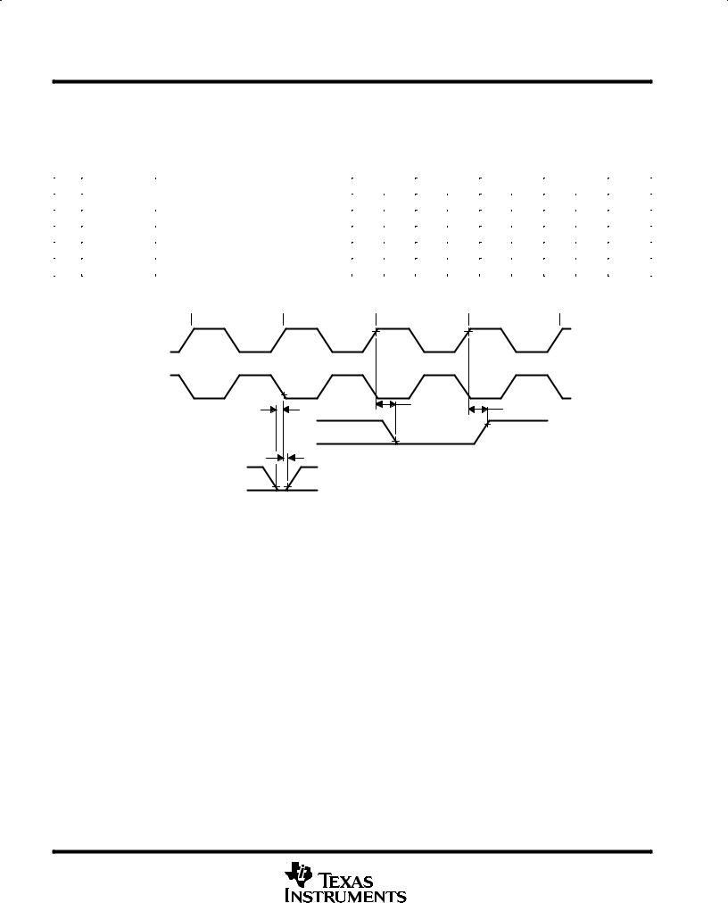
Figure 8. Timing for H1 and H3
POST OFFICE BOX 1443 •HOUSTON, TEXAS 77251±1443 |
21 |

22
77251±1443 TEXAS HOUSTON,• 1443 BOX OFFICE POST
memory read/write timing
The following table defines memory read/write timing parameters for (M)STRB. The numbers shown in Figure 9 and Figure 10 correspond with those in the NO. column of the table.
timing parameters for a memory [(M)STRB = 0] read/write (see Figure 9 and Figure 10)
NO. |
|
|
|
|
|
|
|
|
|
|
|
|
|
|
|
|
|
|
|
'C30-27 |
'C30-33 |
'C30-40 |
'C30-50 |
UNIT |
||||
|
|
|
|
|
|
|
|
|
|
|
|
|
|
|
|
|
|
|
|
|
|
|
|
|
|
|
||
|
|
|
|
|
|
|
|
|
|
|
|
|
|
|
|
|
|
|
MIN |
MAX |
MIN |
MAX |
MIN |
MAX |
MIN |
MAX |
||
|
|
|
|
|
|
|
|
|
|
|
|
|
|
|
|
|
|
|
|
|
||||||||
|
|
|
|
|
|
|
|
|
|
|
|
|
|
|
|
|
|
|
|
|
|
|
|
|
|
|
||
11 |
td[H1L-(M)SL] |
Delay time, H1 low to |
|
|
|
|
|
|
|
low |
0² |
13 |
0² |
10 |
0² |
6³ |
0² |
4 |
ns |
|||||||||
(M)STRB |
||||||||||||||||||||||||||||
12 |
t |
Delay time, H1 low to |
|
|
|
|
|
|
|
|
high |
0² |
13 |
0² |
10 |
0² |
6 |
0² |
4 |
ns |
||||||||
(M)STRB |
||||||||||||||||||||||||||||
|
d[H1L-(M)SH] |
|
|
|
|
|
|
|
|
|
|
|
|
|
|
|
|
|
|
|
|
|
|
|
|
|
|
|
13.1 |
td(H1H-RWL) |
|
|
|
|
|
|
|
|
|
|
|
|
|
|
|
|
|
|
0² |
|
0² |
|
0² |
|
0² |
|
|
Delay time, H1 high to R/W |
low |
13 |
10 |
9 |
7 |
ns |
||||||||||||||||||||||
13.2 |
t |
|
|
|
|
|
|
|
|
|
|
|
|
|
|
|
low |
0² |
19 |
0² |
15 |
0² |
13 |
0² |
11 |
ns |
||
Delay time, H1 high to XR/W |
||||||||||||||||||||||||||||
|
d(H1H-XRWL) |
|
|
|
|
|
|
|
|
|
|
|
|
|
|
|
|
|
|
|
|
|
|
|
|
|
|
|
14.1 |
td(H1L-A) |
Delay time, H1 low to A valid |
0² |
16 |
0² |
14 |
0² |
11 |
0² |
9 |
ns |
|||||||||||||||||
14.2 |
td(H1L-XA) |
Delay time, H1 low to XA valid |
0² |
12 |
0² |
10 |
0² |
9 |
0² |
8 |
ns |
|||||||||||||||||
15.1 |
tsu(D-H1L)R |
Setup time, D before H1 low (read) |
18 |
|
16 |
|
14 |
|
10 |
|
ns |
|||||||||||||||||
15.2 |
tsu(XD-H1L)R |
Setup time, XD before H1 low (read) |
21 |
|
18 |
|
16 |
|
14 |
|
ns |
|||||||||||||||||
16 |
th[H1L-(X)D]R |
Hold time, (X)D after H1 low (read) |
0 |
|
0 |
|
0 |
|
0 |
|
ns |
|||||||||||||||||
|
|
|
|
|
|
|
|
|
|
|
|
|
|
|
|
|
|
|
|
|||||||||
17.1 |
tsu(RDY-H1H) |
Setup time, |
RDY |
before H1 high |
10 |
|
8 |
|
8 |
|
6 |
|
ns |
|||||||||||||||
17.2 |
tsu(XRDY-H1H) |
Setup time, |
|
|
|
|
|
before H1 high |
11 |
|
9 |
|
9 |
|
8 |
|
ns |
|||||||||||
XRDY |
|
|
|
|
|
|||||||||||||||||||||||
18 |
th[H1H-(X)RDY] |
Hold time, |
|
|
|
|
|
|
after H1 high |
0 |
|
0 |
|
0 |
|
0 |
|
ns |
||||||||||
(X)RDY |
|
|
|
|
||||||||||||||||||||||||
19 |
td[H1H-(X)RWH]W |
|
|
|
|
|
|
|
|
|
|
|
|
|
|
|
|
high (write) |
|
13 |
|
10 |
|
9 |
|
7 |
ns |
|
Delay time, H1 high to (X)R/W |
|
|
|
|
||||||||||||||||||||||||
20 |
tv[H1L-(X)D]W |
Valid time, (X)D after H1 low (write) |
|
25 |
|
20 |
|
17 |
|
14 |
ns |
|||||||||||||||||
21 |
t |
Hold time, (X)D after H1 high (write) |
0² |
|
0² |
|
0² |
|
0² |
|
ns |
|||||||||||||||||
|
h[H1H-(X)D]W |
|
|
|
|
|
|
|
|
|
|
|
|
|
|
|
|
|
|
|
|
|
|
|
|
|
|
|
22.1 |
td(H1H-A)W |
Delay time, H1 high to A valid on back-to-back write cycles (write) |
|
23 |
|
18 |
|
15 |
|
12 |
ns |
|||||||||||||||||
22.2 |
td(H1H-XA)W |
Delay time, H1 high to XA valid on back-to-back write cycles (write) |
|
32 |
|
25 |
|
21 |
|
18 |
ns |
|||||||||||||||||
26 |
t |
Delay time, |
|
|
|
|
from A valid |
|
10§ |
|
8§ |
|
7§ |
|
6 |
ns |
||||||||||||
(X)RDY |
|
|
|
|
||||||||||||||||||||||||
|
d[A-(X)RDY] |
|
|
|
|
|
|
|
|
|
|
|
|
|
|
|
|
|
|
|
|
|
|
|
|
|
|
|
² Specified by design but not tested
³ For 'C30 PPM, td[H1L-(M)SL] (max)=7 ns § This value is characterized but not tested
1997 JUNE REVISED ± 1996 APRIL ± SPRS032A |
TMS320C30 PROCESSOR SIGNAL DIGITAL |

TMS320C30
DIGITAL SIGNAL PROCESSOR
SPRS032A ± APRIL 1996 ± REVISED JUNE 1997
memory read/write timing (continued)
H3
H1
11 |
12 |
(M)STRB (see Note A)
(X)R/W
14.1/14.2 |
13.1/13.2 |
|
(X)A |
|
|
15.1/15.2 |
26 |
16 |
|
(X)D
17.1/17.2
18
(X)RDY
NOTE A: (M)STRB remains low during back-to-back read operations.
Figure 9. Timing for Memory [(M)STRB = 0] Read
H3 |
|
H1 |
|
11 |
12 |
|
|
(M)STRB |
|
13.1/13.2 |
19 |
|
|
(X)R/W |
|
14.1/14.2 |
|
|
22.1/22.2 |
(X)A |
|
20 |
21 |
(X)D |
|
18
17.1/17.2
(X)RDY
Figure 10. Timing for Memory [(M)STRB = 0] Write
POST OFFICE BOX 1443 •HOUSTON, TEXAS 77251±1443 |
23 |

TMS320C30
DIGITAL SIGNAL PROCESSOR
SPRS032A ± APRIL 1996 ± REVISED JUNE 1997
memory read/write timing (continued)
The following table defines memory read timing parameters for IOSTRB. The numbers shown in Figure 11 correspond with those in the NO. column of the table below.
timing parameters for a memory (IOSTRB = 0) read (see Figure 11)
NO. |
|
|
|
|
|
|
|
|
|
|
|
|
|
|
|
|
|
|
|
|
|
|
|
|
|
|
|
|
|
|
|
|
|
'C30-27 |
|
|
|
|
'C30-33 |
|
|
|
'C30-40 |
'C30-50 |
UNIT |
||||||||||||||||||||||||||||||||||||
|
|
|
|
|
|
|
|
|
|
|
|
|
|
|
|
|
|
|
|
|
|
|
|
|
|
|
|
|
|
|
|
|
|
|
|
|
|
|
|
|
|
|
|
|
|
|
|
|
|
|
|
|
|
|
|
|
|
|
|
|
|
|
|
|
|
|
|
|
|
|
|
|
|
|
|
|
|
|
|
||
|
|
|
|
|
|
|
|
|
|
|
|
|
|
|
|
|
|
|
|
|
|
|
|
|
|
|
|
|
|
|
|
MIN |
|
MAX |
|
|
|
|
MIN |
|
|
|
|
|
|
|
MAX |
|
|
MIN |
MAX |
MIN |
MAX |
||||||||||||||||||||||||||||
|
|
|
|
|
|
|
|
|
|
|
|
|
|
|
|
|
|
|
|
|
|
|
|
|
|
|
|
|
|
|
|
|
|
|
|
|
|
|
|
|
|
|
|
|
|
|
|
||||||||||||||||||||||||||||||||||
|
|
|
|
|
|
|
|
|
|
|
|
|
|
|
|
|
|
|
|
|
|
|
|
|
|
|
|
|
|
|
|
|
|
|
|
|
|
|
|
|
|
|
|
|
|
|
|
|
|
|
|
|
|
|
|
|
|
|
|
|
|
|
|
|
|
|
|
|
|
|
|
|
|
|
|
|
|
|
|
||
|
|
Delay time, H1 high to |
|
|
|
|
|
|
|
|
|
|
|
|
|
|
|
|
|
|
|
|
|
|
|
|
|
|
|
|
|
|
|
|
|
|
|
|
|
|
|
|
|
|
|
|
|
|
|
|
|
|
|
|
|
|
|
|
|
|
|
|
|
|
|
|
|||||||||||||||
11.1 |
td(H1H-IOSL) |
IOSTRB |
|
|
|
|
0² |
13 |
0² |
10 |
|
|
|
0² |
|
9 |
0² |
8 |
ns |
||||||||||||||||||||||||||||||||||||||||||||||||||||||||||||||
low |
|
|
|
|
|||||||||||||||||||||||||||||||||||||||||||||||||||||||||||||||||||||||||||||
|
|
|
|
|
|
|
|
|
|
|
|
|
|
|
|
|
|
|
|
|
|
|
|
|
|
|
|
|
|
|
|
|
|
|
|
|
|
|
|
|
|
|
|
|
|
|
|
|
|
|
|||||||||||||||||||||||||||||||
|
|
|
|
|
|
|
|
|
|
|
|
|
|
|
|
|
|
|
|
|
|
|
|
|
|
|
|
|
|
|
|
|
|
|
|
|
|
|
|
|
|
|
|
|
|
|
|
|
|
|
|
|
|
|
|
|
|
|
|
|
|
|
|
|
|
|
|
|
|
|
|
|
|
|
|
|
|
|
|
||
|
|
Delay time, H1 high to |
|
|
|
|
|
|
|
|
|
|
|
|
|
|
|
|
|
|
|
|
|
|
|
|
|
|
|
|
|
|
|
|
|
|
|
|
|
|
|
|
|
|
|
|
|
|
|
|
|
|
|
|
|
|
|
|
|
|
|
|
|
|
|
|
|||||||||||||||
12.1 |
td(H1H-IOSH) |
IOSTRB |
|
|
|
|
0² |
13 |
0² |
10 |
|
|
|
0² |
|
9 |
0² |
8 |
ns |
||||||||||||||||||||||||||||||||||||||||||||||||||||||||||||||
high |
|
|
|
|
|||||||||||||||||||||||||||||||||||||||||||||||||||||||||||||||||||||||||||||
|
|
|
|
|
|
|
|
|
|
|
|
|
|
|
|
|
|
|
|
|
|
|
|
|
|
|
|
|
|
|
|
|
|
|
|
|
|
|
|
|
|
|
|
|
|
|
|
|
|
|
|||||||||||||||||||||||||||||||
|
|
|
|
|
|
|
|
|
|
|
|
|
|
|
|
|
|
|
|
|
|
|
|
|
|
|
|
|
|
|
|
|
|
|
|
|
|
|
|
|
|
|
|
|
|
|
|
|
|
|
|
|
|
|
|
|
|
|
|
|
|
|
|
|
|
|
|
|
|
|
|
|
|
|
|
|
|
|
|||
13.1 |
td(H1L-XRWH) |
|
|
|
|
|
|
|
|
|
|
|
|
|
|
|
|
|
|
|
|
|
|
|
|
|
|
|
|
|
|
|
0² |
|
|
|
|
|
|
|
|
|
|
|
|
0² |
|
|
|
|
|
|
|
|
|
|
|
|
|
|
|
|
0² |
|
|
|
|
|
|
||||||||||||
Delay time, H1 low to XR/W |
high |
13 |
10 |
|
|
|
|
9 |
0 |
8 |
ns |
||||||||||||||||||||||||||||||||||||||||||||||||||||||||||||||||||||||
14.3 |
t |
Delay time, H1 low to XA valid |
0² |
13 |
0² |
10 |
|
|
|
0² |
|
9 |
0² |
8 |
ns |
||||||||||||||||||||||||||||||||||||||||||||||||||||||||||||||||||
|
d(H1L-XA) |
|
|
|
|
|
|
|
|
|
|
|
|
|
|
|
|
|
|
|
|
|
|
|
|
|
|
|
|
|
|
|
|
|
|
|
|
|
|
|
|
|
|
|
|
|
|
|
|
|
|
|
|
|
|
|
|
|
|
|
|
|
|
|
|
|
|
|
|
|
|
|
|
|
|
|
|
|
|
|
|
15.3 |
tsu(XD-H1H)R |
Setup time, XD before H1 high |
19 |
|
|
|
|
|
|
|
|
|
|
|
|
15 |
|
|
|
|
|
|
|
|
|
|
|
|
|
|
|
|
13 |
|
|
11 |
|
ns |
|||||||||||||||||||||||||||||||||||||||||||
(read) |
|
|
|
|
|
|
|
|
|
|
|
|
|
|
|
|
|
|
|
|
|
|
|
|
|
|
|
|
|
|
|
||||||||||||||||||||||||||||||||||||||||||||||||||
|
|
|
|
|
|
|
|
|
|
|
|
|
|
|
|
|
|
|
|
|
|
|
|
|
|
|
|
|
|
|
|
|
|
|
|
|
|
|
|
|
|
|
|
|
|
|
|
|
|
|
|||||||||||||||||||||||||||||||
|
|
|
|
|
|
|
|
|
|
|
|
|
|
|
|
|
|
|
|
|
|
|
|
|
|
|
|
|
|
|
|
|
|
|
|
|
|
|
|
|
|
|
|
|
|
|
|
|
|
|
|
|
|
|
|
|
|
|
|
|
|
|
|
|
|
|
|
|
|
|
|
|
|
|
|
|
|
|
|||
16.1 |
thH1H-XD)R |
Hold time, XD after H1 high (read) |
0 |
|
|
|
|
|
|
|
|
|
|
|
|
0 |
|
|
|
|
|
|
|
|
|
|
|
|
|
|
|
|
0 |
|
|
0 |
|
ns |
|||||||||||||||||||||||||||||||||||||||||||
|
|
|
|
|
|
|
|
|
|
|
|
|
|
|
|
|
|
|
|
|
|
|
|
|
|
|
|
|
|
|
|
|
|
|
|
|
|
|
|
|
|
|
|
|
|
|
|
|
|
|
|
|
|
|
|
|
|
|
|
|
|
|
|
|
|
|
|
|
|
|
|
|
|
|
|
|
|
||||
17.3 |
tsu(XRDY-H1H) |
Setup time, |
XRDY |
before H1 high |
11 |
|
|
|
|
|
|
|
|
|
|
|
|
9 |
|
|
|
|
|
|
|
|
|
|
|
|
|
|
|
|
9 |
|
|
8 |
|
ns |
|||||||||||||||||||||||||||||||||||||||||
18.1 |
th(H1H-XRDY) |
Hold time, |
|
|
|
|
|
|
after H1 high |
0 |
|
|
|
|
|
|
|
|
|
|
|
|
0 |
|
|
|
|
|
|
|
|
|
|
|
|
|
|
|
|
0 |
|
|
0 |
|
ns |
||||||||||||||||||||||||||||||||||||
XRDY |
|
|
|
|
|
|
|
|
|
|
|
|
|
|
|
|
|
|
|
|
|
|
|
|
|
|
|
|
|
|
|
|
|
||||||||||||||||||||||||||||||||||||||||||||||||
23 |
td(H1L-XRWL) |
|
|
|
|
|
|
|
|
|
|
|
|
|
|
|
|
|
|
|
|
|
|
|
|
|
|
|
|
|
|
|
0² |
|
|
|
|
|
|
|
|
|
|
|
|
0² |
|
|
|
|
|
|
|
|
|
|
|
|
|
|
|
|
0² |
|
|
|
0² |
|
|
||||||||||||
Delay time, H1 low to XR/W |
low |
19 |
15 |
|
|
|
|
13 |
11 |
ns |
|||||||||||||||||||||||||||||||||||||||||||||||||||||||||||||||||||||||
² This value is characterized but not tested |
|
|
|
|
|
|
|
|
|
|
|
|
|
|
|
|
|
|
|
|
|
|
|
|
|
|
|
|
|
|
|
|
|
|
|
|
|
|
|
|
|
|
|
|
|
|
|
|
|
||||||||||||||||||||||||||||||||
|
|
|
|
H3 |
|
|
|
|
|
|
|
|
|
|
|
|
|
|
|
|
|
|
|
|
|
|
|
|
|
|
|
|
|
|
|
|
|
|
|
|
|
|
|
|
|
|
|
|
|
|
|
|
|
||||||||||||||||||||||||||||
|
|
|
|
|
|
|
|
|
|
|
|
|
|
|
|
|
|
|
|
|
|
|
|
|
|
|
|
|
|
|
|
|
|
|
|
|
|
|
|
|
|
|
|
|
|
|
|
|
|
|
|
|
|
|
|
|
|
|
|
|
|
|
|
|
|||||||||||||||||
|
|
|
|
H1 |
|
|
|
|
|
|
|
|
|
|
|
|
|
|
|
|
|
|
|
|
|
|
|
|
|
|
|
|
|
|
|
|
|
|
|
|
|
|
|
|
|
|
|
|
|
|
|
|
|
|
|
||||||||||||||||||||||||||
|
|
|
|
|
|
|
|
|
|
|
|
|
|
|
|
|
|
|
|
|
|
|
|
|
|
|
|
|
|
|
|
|
|
|
|
|
|
|
|
|
|
|
|
|
|
|
|
|
|
|
|
|
|
|
|
|
|
|
|
|
|
|
|
|
|
|
|
|
|
|
|||||||||||
|
|
11.1 |
|
|
|
|
|
|
|
|
|
|
|
|
|
|
12.1 |
|
|
|
|
|
|
|
|
|
|
|
|
|
|
|
|
|
|
|
|
|
|
|
|
|
|
|
|
|
|
|
|
|
|
|
|
|
|
|
|
|
|||||||||||||||||||||||
|
|
|
|
|
|
|
|
|
|
|
|
|
|
|
|
|
|
|
|
|
|
|
|
|
|
|
|
|
|
|
|
|
|
|
|
|
|
|
|
|
|
|
|
|
|
|
|
|
|
|
|
|
|
||||||||||||||||||||||||||||
|
|
|
|
|
|
|
|
|
|
|
|
|
|
|
|
|
|
|
|
|
|
|
|
|
|
|
|
|
|
|
|
|
|
|
|
|
|
|
|
|
|
|
|
|
|
|
|
|
|
|
|
|
|
|
|
|
|
||||||||||||||||||||||||
|
|
|
IOSTRB |
|
|
|
|
|
|
|
|
|
|
|
|
|
|
|
|
|
|
|
|
|
|
|
|
|
|
|
|
|
|
|
|
|
|
|
|
|
|
|
|
|
|
|
|
|
|
|
|
|
|
|
|
||||||||||||||||||||||||||
|
|
|
|
|
|
|
|
|
|
|
|
|
|
|
|
|
|
|
|
|
|
13.1 |
|
|
|
|
|
|
|
|
|
|
|
|
|
|
|
|
|
|
|
|
|
|
|
|
|
|
|
|
|
|
|
|
|
|
|
|
|
|
|
|
|
|
|
|
|
|
|
23 |
|
|
|
|
|||||||
|
|
|
|
|
|
|
|
|
|
|
|
|
|
|
|
|
|
|
|
|
|
|
|
|
|
|
|
|
|
|
|
|
|
|
|
|
|
|
|
|
|
|
|
|
|
|
|
|
|
|
|
|
|
|
|
|
|
|
|
|
|
|
|
|
|
|
|
|
|
|
|
|
|||||||||
|
|
|
|
|
|
|
|
|
|
|
|
|
|
|
|
|
|
|
|
|
|
|
|
|
|
|
|
|
|
|
|
|
|
|
|
|
|
|
|
|
|
|
|
|
|
|
|
|
|
|
|
|
|
|
|
|
|
|
|
|
|
|
|
|
|
|
|
|
|
||||||||||||
|
|
|
|
|
|
|
|
|
|
|
|
|
|
|
|
|
|
|
|
|
|
|
|
|
|
|
|
|
|
|
|
|
|
|
|
|
|
|
|
|
|
|
|
|
|
|
|
|
|
|
|
|
|
|
|
|
|
|
|
||||||||||||||||||||||
|
|
|
|
|
|
|
|
|
|
|
|
|
|
|
|
|
|
|
|
|
|
|
|
|
|
|
|
|
|
|
|
|
|
|
|
|
|
|
|
|
|
|
|
|
|
|
|
|
|
|
|
|
|
|
|
|
|
|
|
|
|
|
|
|
|
|
|
|
|
|
|
|
|||||||||
|
|
|
|
|
|
|
|
|
|
|
|
|
|
|
|
|
|
|
|
|
|
|
|
|
|
|
|
|
|
|
|
|
|
|
|
|
|
|
|
|
|
|
|
|
|
|
|
|
|
|
|
|
|
|
|
|
|
|
|
|
|
|
|
|
|
|
|
|
|
|
|
|
|
|
|
|
|||||
|
|
|
|
XR/W |
|
|
|
|
|
|
|
|
|
|
|
|
|
|
|
|
|
|
|
|
|
|
|
|
|
|
|
|
|
|
|
|
|
|
|
|
|
|
|
|
|
|
|
|
|
|
|
|
|
|
|
|
|||||||||||||||||||||||||
|
|
|
|
|
|
|
|
|
|
|
|
|
|
|
|
|
|
|
|
|
14.3 |
|
|
|
|
|
|
|
|
|
|
|
|
|
|
|
|
|
|
|
|
|
|
|
|
|
|
|
|
|
|
|
|
|
|
|
|
|
|
|
|
|
|
|
|
|
|
|
|
|
|
|
|||||||||
|
|
|
|
|
|
|
|
|
|
|
|
|
|
|
|
|
|
|
|
|
|
|
|
|
|
|
|
|
|
|
|
|
|
|
|
|
|
|
|
|
|
|
|
|
|
|
|
|
|
|
|
|
|
|
|
|
|
|
|
|
|
|
|
|
|
|
|
|
|
|
|
||||||||||
|
|
|
|
|
|
|
|
|
|
|
|
|
|
|
|
|
|
|
|
|
|
|
|
|
|
|
|
|
|
|
|
|
|
|
|
|
|
|
|
|
|
|
|
|
|
|
|
|
|
|
|
|
|
|
|
|
|
|
|||||||||||||||||||||||
|
|
|
|
|
|
|
|
|
|
|
|
|
|
|
|
|
|
|
|
|
|
|
|
|
|
|
|
|
|
|
|
|
|
|
|
|
|
|
|
|
|
|
|
|
|
|
|
|
|
|
|
|
|
|
|
|
|
|
|
|
|
|
|
|
|
|
|
|
|
|
|
||||||||||
|
|
|
|
|
|
|
|
|
|
|
|
|
|
|
|
|
|
|
|
|
|
|
|
|
|
|
|
|
|
|
|
|
|
|
|
|
|
|
|
|
|
|
|
|
|
|
|
|
|
|
|
|
|
|
|
|
|
|
|
|
|
|
|
|
|
|
|
|
|
|
|
|
|
|
|
|
|
|
|
|
|
|
|
|
|
XA |
|
|
|
|
|
|
|
|
|
|
|
|
|
|
|
|
|
|
|
|
|
|
|
|
|
|
|
|
|
|
|
|
|
|
|
|
|
|
|
|
|
|
|
|
|
|
|
|
|
||||||||||||||||||||||||||||
|
|
|
|
|
|
|
|
|
|
|
|
|
|
|
|
|
|
|
|
|
|
|
|
|
|
|
|
|
|
|
|
|
|
|
|
|
|
|
|
|
|
|
|
|
|
|
|
|
|
|
|
|
|
|
|
|
|
|
|
|
|
|
|
|
|
|
|
|
|
|
|
|
|
|
|
|
|
|
|
|
|
|
|
|
|
|
|
|
|
|
|
|
|
|
|
|
|
|
|
|
|
|
|
|
|
|
|
|
|
|
|
|
|
|
|
|
|
|
|
|
|
|
|
|
|
|
|
|
|
|
|
|
|
|
|
|
|
|
|
|
|
|
|
|
|
|
|
|
|
|
|
|
|
|
|
|
|
|
|
|
|
|
|
|
|
|
|
|
|
|
|
|
|
|
|
|
|
|
|
|
|
|
|
|
|
|
|
|
|
|
|
|
|
|
|
|
15.3 |
|
|
|
|
|
|
|
|
|
|
|
|
|
|
|
|
|
|
|
|
|
|
|
|
|
|
|
|
|
|
|
|
|
|
|
|
|
|
|
|
|
|
|
|
|
|
||
|
|
|
|
|
|
|
|
|
|
|
|
|
|
|
|
|
|
|
|
|
|
|
|
|
|
|
|
|
|
|
|
|
|
|
|
|
|
|
|
|
|
|
|
|
|
|
|
|
|
|
|
|
|
|
|
|
|
|
|
|
|
|
|
|
|
|
|
|
|
|
|
|
|
|
|
|
|
||||
|
|
|
|
XD |
|
|
|
|
|
|
|
|
|
|
|
|
|
|
|
|
|
|
|
|
|
|
|
|
|
|
|
|
|
|
|
|
16.1 |
|
|
|
|
|
|
|
|
|
|
|
|||||||||||||||||||||||||||||||||
|
|
|
|
17.3 |
|
|
|
|
|
|
|
|
|
|
|
|
|
|
|
|
|
|
|
|
|
|
|
|
|
|
|
|
|
|
|
|
|
|
|
|
|
|
|
||||||||||||||||||||||||||||||||||||||
|
|
|
|
|
|
|
|
|
|
|
|
|
|
|
|
|
|
|
|
|
|
|
|
|
|
|
|
|
|
|
|
|
|
|
|
|
|
|
|
|
|||||||||||||||||||||||||||||||||||||||||
|
|
|
|
|
|
|
|
|
|
|
|
|
|
|
|
|
|
|
|
|
|
|
|
|
|
|
|
|
|
|
|
|
|
|
18.1 |
|
|
|
|
|
|
|
|
|
|||||||||||||||||||||||||||||||||||||
|
|
|
|
|
|
|
|
|
|
|
|
|
|
|
|
|
|
|
|
|
|
|
|
|
|
|
|
|
|
|
|
|
|
|
|
|
|
|
|
|
|
|
|
||||||||||||||||||||||||||||||||||||||
|
|
|
|
|
|
|
|
|
|
|
|
|
|
|
|
|
|
|
|
|
|
|
|
|
|
|
|
|
|
|
|
|
|
|
|
|
|
|
|
|
|
|
|
|
|
|
|
|
|
|
|
|
|
|
|
|
|
|
|
|
|
|
|
|
|
|
|
|
|
|
|
|
|||||||||
|
|
|
|
|
|
|
|
|
|
|
|
|
|
|
|
|
|
|
|
|
|
|
|
|
|
|
|
|
|
|
|
|
|
|
|
|
|
|
|
|
|
|
|
|
|
|
|
|
|
|
|
|
|
|
|
|
|
|
|
|
|
|
|
|
|
|
|
|
|
|
|
|
|||||||||
|
|
|
|
|
|
|
|
|
|
|
|
|
|
|
|
|
|
|
|
|
|
|
|
|
|
|
|
|
|
|
|
|
|
|
|
|
|
|
|
|
|
|
|
|
|
|
|
|
|
|
|
|
|
|
|
|
|
|
|
|
|
|
|
|
|
|
|
|
|
|
|
|
|||||||||
|
|
|
|
|
|
|
|
|
|
|
|
|
|
|
|
|
|
|
|
|
|
|
|
|
|
|
|
|
|
|
|
|
|
|
|
|
|
|
|
|
|
|
|
|
|
|
|
|
|
|
|
|
|
|
|
|
|
|
|
|
|
|
|
|
|
|
|
|
|||||||||||||
|
|
|
|
|
|
|
|
|
|
|
|
|
|
|
|
|
|
|
|
|
|
|
|
|
|
|
|
|
|
|
|
|
|
|
|
|
|
|
|
|
|
|
|
|
|
|
|
|
|
|
|
|
|
|
|
|
|
|
|
|
|
|
|
|
|
|
|
||||||||||||||
|
|
|
|
|
|
|
|
|
|
|
|
|
|
|
|
|
|
|
|
|
|
|
|
|
|
|
|
|
|
|
|
|
|
|
|
|
|
|
|
|
|
|
|
|
|
|
|
|
|
|
|
|
|
|
|||||||||||||||||||||||||||
|
|
|
|
(X)RDY |
|
|
|
|
|
|
|
|
|
|
|
|
|
|
|
|
|
|
|
|
|
|
|
|
|
|
|
|
|
|
|
|
|
|
|
|
|
|
|
|
|
|
|
|
|
|
|
|
|
|
|
|
|||||||||||||||||||||||||
|
|
|
|
|
|
|
|
|
|
|
|
|
|
|
|
|
|
|
|
|
|
|
|
|
|
|
|
|
|
|
|
|
|
|
|
|
|
|
|
|
|
|
|
|
|
|
|
|
|
|
|
|
|
|
|
|
|
|
|
|
|
|
|
|
|
|
|
|
|
|
|
|
|
|
|
|
|
|
|
|
|
|
|
|
|
|
|
|
|
|
|
|
|
|
|
|
|
|
|
|
|
|
|
|
|
|
|
|
|
|
|
|
|
|
|
|
|
|
|
|
|
|
|
|
|
|
|
|
|
|
|
|
|
|
|
|
|
|
|
|
|
|
|
|
|
|
|
|
|
|
|
|
|
|
|
|
|
|
|
|
|
|
|
Figure 11. Timing for Memory (IOSTRB = 0) Read
24 |
POST OFFICE BOX 1443 •HOUSTON, TEXAS 77251±1443 |

TMS320C30
DIGITAL SIGNAL PROCESSOR
SPRS032A ± APRIL 1996 ± REVISED JUNE 1997
memory read/write timing (continued)
The following table defines memory write timing parameters for IOSTRB. The numbers shown in Figure 12 correspond with those in the NO. column of the table below.
timing parameters for a memory (IOSTRB = 0) write (see Figure 12)
NO. |
|
|
|
|
|
|
|
|
|
|
|
|
'C30-27 |
'C30-33 |
'C30-40 |
'C30-50 |
UNIT |
||||
|
|
|
|
|
|
|
|
|
|
|
|
|
|
|
|
|
|
|
|
||
|
|
|
|
|
|
|
|
|
|
|
|
MIN |
MAX |
MIN |
MAX |
MIN |
MAX |
MIN |
MAX |
||
|
|
|
|
|
|
|
|
|
|
|
|
|
|
||||||||
|
|
|
|
|
|
|
|
|
|
|
|
|
|
|
|
|
|
|
|
||
11.1 |
td(H1H-IOSL) |
Delay time, H1 high to |
|
|
|
|
low |
0² |
13 |
0² |
10 |
0² |
9 |
0² |
8 |
ns |
|||||
IOSTRB |
|||||||||||||||||||||
12.1 |
td(H1H-IOSH) |
Delay time, H1 high to |
|
|
|
|
|
high |
0² |
13 |
0² |
10 |
0² |
9 |
0² |
8 |
ns |
||||
IOSTRB |
|||||||||||||||||||||
13.1 |
td(H1L-XRWH) |
|
|
|
|
|
|
|
|
|
|
|
0² |
|
0² |
|
0² |
|
|
|
|
Delay time, H1 low to XR/W |
high |
13 |
10 |
9 |
0 |
8 |
ns |
||||||||||||||
14.3 |
t |
Delay time, H1 low to XA valid |
0² |
13 |
0² |
10 |
0² |
9 |
0² |
8 |
ns |
||||||||||
|
d(H1L-XA) |
|
|
|
|
|
|
|
|
|
|
|
|
|
|
|
|
|
|
|
|
17.3 |
tsu(XRDY-H1H) |
Setup time, |
|
|
before H1 high |
11 |
|
9 |
|
9 |
|
8 |
|
ns |
|||||||
XRDY |
|
|
|
|
|||||||||||||||||
18.1 |
th(H1H-XRDY) |
Hold time, |
|
|
after H1 high |
0 |
|
0 |
|
0 |
|
0 |
|
ns |
|||||||
XRDY |
|
|
|
|
|||||||||||||||||
23 |
td(H1L-XRWL) |
|
|
|
|
|
|
|
|
|
|
|
0² |
|
0² |
|
0² |
|
0² |
|
|
Delay time, H1 low to XR/W |
low |
19 |
15 |
13 |
11 |
ns |
|||||||||||||||
24 |
tv(H1H-XD)W |
Valid time, (X)D after H1 high (write) |
|
38 |
|
30 |
|
25 |
|
20 |
ns |
||||||||||
25 |
th(H1L-XD)W |
Hold time, (X)D after H1 low (write) |
0 |
|
0 |
|
0 |
|
0 |
|
ns |
||||||||||
² This value is characterized but not tested
H3
H1
11.1 |
12.1 |
IOSTRB
13.1
23
(X)R/W
14.3
(X)A
24 |
25 |
(X)D
17.3
18.1
(X)RDY
Figure 12. Timing for Memory (IOSTRB = 0) Write
POST OFFICE BOX 1443 •HOUSTON, TEXAS 77251±1443 |
25 |

TMS320C30
DIGITAL SIGNAL PROCESSOR
SPRS032A ± APRIL 1996 ± REVISED JUNE 1997
XF0 and XF1 timing when executing LDFI or LDII
The following table defines the timing parameters for XF0 and XF1 during execution of LDFI or LDII. The numbers shown in Figure 13 correspond with those in the NO. column of the table below.
timing parameters for XF0 and XF1 when executing LDFI or LDII (see Figure 13)
NO. |
|
|
'C30-27 |
'C30-33 |
'C30-40 |
'C30-50 |
UNIT |
|
|
|
|
|
|
||
|
|
MIN MAX |
MIN MAX |
MIN MAX |
MIN MAX |
||
|
|
|
|
||||
|
|
|
|
|
|
|
|
1 |
td(H3H-XF0L) |
Delay time, H3 high to XF0 low |
19 |
15 |
13 |
12 |
ns |
2 |
tsu(XF1-H1L) |
Setup time, XF1 before H1 low |
13 |
10 |
9 |
9 |
ns |
3 |
th(H1L-XF1) |
Hold time, XF1 after H1 low |
0 |
0 |
0 |
0 |
ns |
Fetch |
Decode |
Read |
Execute |
LDFI or LDII |
|||
H3 |
|
|
|
H1 |
|
|
|
(M)STRB
(X)R/W
(X)A
(X)D
(X)RDY
1
XF0 Pin |
2 |
3
XF1 Pin
Figure 13. Timing for XF0 and XF1 When Executing LDFI or LDII
26 |
POST OFFICE BOX 1443 •HOUSTON, TEXAS 77251±1443 |

TMS320C30
DIGITAL SIGNAL PROCESSOR
SPRS032A ± APRIL 1996 ± REVISED JUNE 1997
XF0 timing when executing STFI and STII
The following table defines the timing parameters for the XF0 pin during execution of STFI or STII. The number shown in Figure 14 corresponds with the number in the NO. column of the table below.
timing parameters for XF0 when executing STFI or STII (see Figure 14)
NO. |
|
'C30-27 |
'C30-33 |
'C30-40 |
'C30-50 |
UNIT |
|
|
|
|
|
|
|
||
|
MIN |
MAX |
MIN MAX |
MIN MAX |
MIN MAX |
||
|
|
|
|||||
|
|
|
|
|
|
|
|
1 |
td(H3H-XF0H) Delay time, H3 high to XF0 high |
|
19 |
15 |
13 |
12 |
ns |
XF0 is always set high at the beginning of the execute phase of the interlock store instruction. When no pipeline conflicts occur, the address of the store is also driven at the beginning of the execute phase of the interlock store instruction. However, if a pipeline conflict prevents the store from executing, the address of the store will not be driven until the store can execute.
Fetch |
Decode |
|
|
STFI or STII |
Read |
Execute |
H3
H1
(M)STRB
(X)R/W
(X)A
(X)D
(X)RDY |
1 |
XF0 Pin
Figure 14. Timing for XF0 When Executing an STFI or STII
POST OFFICE BOX 1443 •HOUSTON, TEXAS 77251±1443 |
27 |
TMS320C30
DIGITAL SIGNAL PROCESSOR
SPRS032A ± APRIL 1996 ± REVISED JUNE 1997
XF0 and XF1 timing when executing SIGI
The following table defines the timing parameters for the XF0 and XF1 pins during execution of SIGI. The numbers shown in Figure 15 correspond with those in the NO. column of the table below.
timing parameters for XF0 and XF1 when executing SIGI (see Figure 15)
NO. |
|
|
'C30-27 |
'C30-33 |
'C30-40 |
'C30-50 |
UNIT |
|
|
|
|
|
|
||
|
|
MIN MAX |
MIN MAX |
MIN MAX |
MIN MAX |
||
|
|
|
|
||||
|
|
|
|
|
|
|
|
1 |
td(H3H-XF0L) |
Delay time, H3 high to XF0 low |
19 |
15 |
13 |
12 |
ns |
2 |
td(H3H-XF0H) |
Delay time, H3 high to XF0 high |
19 |
15 |
13 |
12 |
ns |
3 |
tsu(XF1-H1L) |
Setup time, XF1 before H1 low |
13 |
10 |
9 |
9 |
ns |
4 |
th(H1L-XF1) |
Hold time, XF1 after H1 low |
0 |
0 |
0 |
0 |
ns |
Fetch |
|
|
|
SIGI |
Decode |
Read |
Execute |
H3 |
|
|
|
H1 |
|
|
|
3 |
|
1 |
2 |
|
|
||
XF0 |
|
|
|
|
4 |
|
|
XF1 |
|
|
|
Figure 15. Timing for XF0 and XF1 When Executing SIGI
28 |
POST OFFICE BOX 1443 •HOUSTON, TEXAS 77251±1443 |

TMS320C30
DIGITAL SIGNAL PROCESSOR
SPRS032A ± APRIL 1996 ± REVISED JUNE 1997
loading when XFx is configured as an output
The following table defines the timing parameter for loading the XF register when the XFx pin is configured as an output. The number shown in Figure 16 corresponds with the number in the NO. column of the table below.
timing parameters for loading the XFx register when configured as an output pin (see Figure 16)
NO. |
'C30-27 |
'C30-33 |
'C30-40 |
'C30-50 |
UNIT |
||
MIN |
MAX |
MIN MAX |
MIN MAX |
MIN MAX |
|||
|
|
||||||
1 tv(H3H-XF) Valid time, H3 high to XFx |
|
19 |
15 |
13 |
12 |
ns |
|
Fetch Load |
|
|
|
|
|
|
|
Instruction |
Decode |
Read |
Execute |
|
|
||
H3 |
|
|
|
|
|
|
|
H1 |
|
|
|
|
|
|
|
OUTXF |
|
|
|
1 or 0 |
|
||
Bit |
|
|
|
|
|||
|
|
|
|
|
|
||
(see Note A) |
|
|
|
|
1 |
|
|
|
|
|
|
|
|
||
XFx |
|
|
|
|
|
|
|
NOTE A: OUTXFx represents either bit 2 or 6 of the IOF register.
Figure 16. Timing for Loading XFx Register When Configured as an Output Pin
POST OFFICE BOX 1443 •HOUSTON, TEXAS 77251±1443 |
29 |

TMS320C30
DIGITAL SIGNAL PROCESSOR
SPRS032A ± APRIL 1996 ± REVISED JUNE 1997
changing XFx from an output to an input
The following table defines the timing parameters for changing the XFx pin from an output pin to an input pin. The numbers shown in Figure 17 correspond with those in the NO. column of the table below.
timing parameters of XFx changing from output to input mode (see Figure 17)
NO. |
|
|
'C30-27 |
'C30-33 |
'C30-40 |
'C30-50 |
UNIT |
|
|
|
|
|
|
|
|
||
|
|
MIN MAX |
MIN MAX |
MIN |
MAX |
MIN MAX |
||
|
|
|
|
|||||
|
|
|
|
|
|
|
|
|
1 |
t |
Hold time, XFx after H3 high |
19³ |
15³ |
|
13²³ |
12³ |
ns |
|
h(H3H-XF) |
|
|
|
|
|
|
|
2 |
tsu(XF-H1L) |
Setup time, XFx before H1 low |
13 |
10 |
9 |
|
9 |
ns |
3 |
th(H1L-XF) |
Hold time, XFx after H1 low |
0 |
0 |
0 |
|
0 |
ns |
² |
For 'C30 PPM, tn(H3H-XF01) (max)=14 ns |
|
|
|
|
³ |
This value is characterized but not tested |
|
|
|
|
|
|
Execute |
Buffers Go |
Synchronizer |
Value on |
|
|
Load of |
From Output |
Delay |
Pin |
|
|
IOF |
to Output |
|
Seen in IOF |
|
H3 |
|
|
|
|
|
H1 |
|
|
|
|
|
I / OXFx |
|
|
2 |
|
|
|
|
3 |
|
|
|
Bit |
|
|
|
|
|
(see Note A) |
|
1 |
|
|
|
|
|
|
|
|
|
XFx |
Output |
|
|
|
|
INXF Bit |
|
Data |
|
|
|
(see Note A) |
|
Sampled |
|
|
|
|
|
|
|
Data |
|
|
|
|
|
Seen |
NOTE A: I / OXFx represents bit 1 or 5 of the IOF register, and INXFx represents either bit 3 or bit 7 of the IOF register.
Figure 17. Timing for Change of XFx From Output to Input Mode
30 |
POST OFFICE BOX 1443 •HOUSTON, TEXAS 77251±1443 |