

|
|
|
|
|
|
|
|
TMS320C30 |
|
|
|
|
|
|
DIGITAL SIGNAL PROCESSOR |
||||
|
|
|
|
|
|
SPRS032A ± APRIL 1996 ± REVISED JUNE 1997 |
|||
|
|
|
|
|
|
|
|
|
|
|
|
|
|
|
TMS320C30 Pin Functions (Continued) |
|
|
||
|
|
|
|
|
|
|
|
|
|
|
|
PIN |
|
TYPE² |
DESCRIPTION |
CONDITIONS |
|
||
NAME |
QTY³ |
WHEN |
|
||||||
|
|
|
|
SIGNAL IS Z TYPE§ |
|
||||
|
|
|
|
|
SUPPLY AND OSCILLATOR SIGNALS (CONTINUED) |
|
|
||
|
|
|
|
|
|
|
|
|
|
VBBP |
1 |
NC |
VBB pump oscillator output |
|
|
||||
VSUBS |
1 |
I |
Substrate terminal. Tie to ground. |
|
|
||||
X1 |
1 |
O |
Output from the internal oscillator for the crystal. If a crystal is not used, X1 |
|
|
||||
should be left unconnected. |
|
|
|||||||
|
|
|
|
|
|
|
|||
|
|
|
|
|
|
|
|
|
|
X2 / CLKIN |
1 |
I |
Input to the internal oscillator from the crystal or a clock |
|
|
||||
|
|
|
|
|
|
|
|
|
|
H1 |
1 |
O / Z |
External H1 clock. H1 has a period equal to twice CLKIN. |
S |
|
||||
|
|
|
|
|
|
|
|
|
|
H3 |
1 |
O / Z |
External H3 clock. H3 has a period equal to twice CLKIN. |
S |
|
||||
|
|
|
|
|
|
|
|
|
|
|
|
|
|
|
RESERVED¶ |
|
|
||
EMU0± EMU2 |
3 |
I |
Reserved. Use pullup resistors to 5 V. |
|
|
||||
|
|
|
|
|
|
|
|
|
|
EMU3 |
1 |
O / Z |
Reserved |
S |
|
||||
|
|
|
|
|
|
|
|
||
|
|
|
|
|
Shutdown high impedance. When active, EMU4 / |
|
shuts down the |
|
|
|
|
|
|
|
SHZ |
|
|
||
|
|
|
|
|
TMS320C30 and places all pins in the high-impedance state. EMU4 / SHZ is |
|
|
||
|
|
|
|
|
used for board-level testing to ensure that no dual-drive conditions occur. |
|
|
||
EMU4/ SHZ |
1 |
I |
|
|
|||||
CAUTION: A low on SHZ corrupts TMS320C30 memory and register |
|
|
|||||||
|
|
|
|
|
|
|
|||
|
|
|
|
|
contents. Reset the device with SHZ high to restore it to a known operating |
|
|
||
|
|
|
|
|
condition. |
|
|
||
|
|
|
|
|
|
||||
EMU5, EMU6 |
2 |
NC |
Reserved |
|
|
||||
|
|
|
|
|
|
||||
RSV10± RSV5 |
6 |
I / O |
Reserved. Use pullup resistors to 5 V. |
|
|
||||
|
|
|
|
|
|
||||
RSV4 ± RSV0 |
5 |
I |
Reserved. Tie pins directly to 5 V. |
|
|
||||
|
|
|
|
|
|
||||
Locator |
1# |
NC |
Reserved |
|
|
||||
² I = input, O = output, Z = high-impedance state. All pins labeled NC have special functions and should not be connected by the user. ³ Quantity is the same for GEL and PPM packages unless otherwise noted.
§ S = SHZ active, H = HOLD active, R = RESET active
¶Follow the connections specified for the reserved pins. Use 18-kΩ ± 22-kΩ pullup resistors for best results. All 5-V supply pins must be connected to a common supply plane, and all ground pins must be connected to a common ground plane.
# For the GEL package only. There is no locator in the PPM package.
POST OFFICE BOX 1443 •HOUSTON, TEXAS 77251±1443 |
11 |
TMS320C30
DIGITAL SIGNAL PROCESSOR
SPRS032A ± APRIL 1996 ± REVISED JUNE 1997
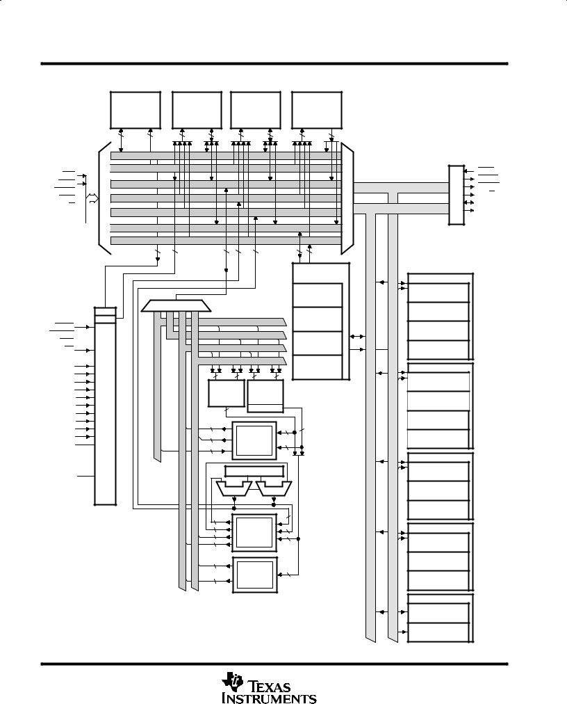
functional block diagram
RDY
HOLD
HOLDA 
STRB 
 R / W
R / W 
D31± D0 

A23 ± A0 
RESET
INT(3 ± 0)  IACK
IACK
MC / MP
XF(1,0)

VDD IODVDD ADVDD PDVDD DDVDD MDVDD
VSS
DVSS
CVSS
IVSS
VBBP
VSUBS  X1
X1
X2 / CLKIN 
H1
H3 EMU(6 ± 0)
 RSV(10 ± 0)

Cache (64 ×32)
|
32 |
24 |
|
|
PDATA Bus |
||
|
|||
|
PADDR Bus |
||
MUX |
DDATA Bus |
||
DADDR1 Bus |
|||
|
|||
|
DADDR2 Bus |
||
|
DMADATA Bus |
||
|
DMAADDR Bus |
||
|
|
32 |
|
|
|
||
IR
PC
CPU1
Controller
RAM |
|
RAM |
ROM |
||
Block 0 |
|
Block 1 |
Block |
||
(1K |
×32) |
|
(1K ×32) |
(4K |
×32) |
24 |
32 |
24 |
32 |
24 |
32 |
MUX
24 |
32 |
24 |
24 |
32 |
24 |
DMA Controller
Global-Control
Register
MUX
|
|
|
|
|
|
|
Source-Address |
|
|
|
|
CPU1 |
|
|
Register |
|
|
|
|
CPU2 |
|
|
Destination- |
|
|
|
|
|
|
|
|
|
|
|
|
REG1 |
|
|
Address |
|
|
|
|
|
|
Register |
|
|
|
|
|
REG2 |
|
|
Transfer- |
|
|
|
|
|
|
|
Counter |
REG1 |
REG2 |
32 |
|
32 |
40 |
40 |
Register |
|
|
||||||
|
|
|
|
32-Bit |
|
||
|
|
|
Multiplier |
|
Barrel |
|
|
|
|
|
|
|
|
Shifter |
|
|
|
|
40 |
|
|
ALU |
|
|
|
|
|
|
|
|
|
|
|
|
40 |
|
|
|
40 |
|
|
|
|
|
|
|
|
|
|
|
40 |
Extended- |
40 |
||
|
|
|
Precision |
|
|||
|
|
|
32 |
Registers |
40 |
||
|
|
|
|
(R7±R0) |
|
||
|
|
|
|
|
|
||
DISP0, IR0, IR1 |
||
ARAU0 |
BK |
ARAU1 |
|
|
|
24 |
|
24 |
|
|
|
24 |
Auxiliary |
24 |
32 |
Registers |
|
(AR0 ± AR7) |
|
|
32 |
|
|
|
32 |
|
|
|
|
32 |
|
|
32 |
Other |
32 |
Registers |
|
|
|
(12) |
|
Peripheral Data Bus |
Peripheral Address Bus |
Serial Port 0
Serial-Port-Control
Register
Receive/Transmit
(R/X) Timer Register
Data-Transmit
Register
Data-Receive
Register
Serial Port 1
Serial-Port-Control
Register
Receive/Transmit
(R/X) Timer Register
Data-Transmit
Register
Data-Receive
Register
Timer 0
Global-Control
Register
Timer-Period
Register
Timer-Counter
Register
Timer 1
Global-Control
Register
Timer-Period
Register
Timer-Counter
Register
Port Control
Primary-Control
Register
Expansion-Control
Register
XRDY
MSTRB
IOSTRB
XR / W XD31±XD0 XA12 ±XA0

 FSX0
FSX0

 DX0
DX0

 CLKX0
CLKX0

 FSR0
FSR0

 DR0
DR0 
 CLKR0
CLKR0

 FSX1
FSX1

 DX1
DX1

 CLKX1
CLKX1

 FSR1
FSR1

 DR1
DR1 
 CLKR1
CLKR1

 TCLK0
TCLK0

 TCLK1
TCLK1
12 |
POST OFFICE BOX 1443 •HOUSTON, TEXAS 77251±1443 |

TMS320C30
DIGITAL SIGNAL PROCESSOR
SPRS032A ± APRIL 1996 ± REVISED JUNE 1997
memory map
Figure 1 depicts the memory map for the TMS320C30. Refer to the TMS320C3x User's Guide (literature number SPRU031) for a detailed description of this memory mapping. Figure 2 shows the reset, interrupt, and trap vector/branches memory-map locations. Figure 3 shows the peripheral bus memory-mapped registers.
0h
03Fh
040h
7FFFFFh
800000h
801FFFh
802000h
803FFFh
804000h
805FFFh
806000h
807FFFh
808000h
8097FFh
809800h
809BFFh
809C00h
809FFFh
80A000h
Reset, Interrupt, Trap
Vectors, and Reserved
Locations (64) (External
STRB Active)
External
STRB Active
(8M Words ± 64 Words)
Expansion-Bus
MSTRB Active
(8K Words)
Reserved
(8K Words)
Expansion-Bus
IOSTRB Active
(8K Words)
Reserved
(8K Words)
Peripheral-Bus
Memory-Mapped
Registers
(6K Words Internal)
RAM Block 0
(1K Word Internal)
RAM Block 1
(1K Word Internal)
External
STRB Active
(8M Words ± 40K Words)
0h
0BFh
0C0h
0FFFh
1000h
7FFFFFh
800000h
801FFFh
802000h
803FFFh
804000h
805FFFh
806000h
807FFFh
808000h
8097FFh
809800h
809BFFh
809C00h
809FFFh
80A000h
Reset, Interrupt,
Trap Vectors, and Reserved
Locations (192)
ROM (Internal)
External
STRB Active
(8M Words ± 4K Words)
Expansion-Bus
MSTRB Active
(8K Words)
Reserved
(8K Words)
Expansion-Bus
IOSTRB Active
(8K Words)
Reserved
(8K Words)
Peripheral-Bus
Memory-Mapped
Registers
(6K Words Internal)
RAM Block 0
(1K Word Internal)
RAM Block 1
(1K Word Internal)
External
STRB Active
(8M Words ± 40K Words)
0FFFFFFh |
|
0FFFFFFh |
|
|
|
||
|
(a) Microprocessor Mode |
(b) Microcomputer Mode |
|
Figure 1. TMS320C30 Memory Map
POST OFFICE BOX 1443 •HOUSTON, TEXAS 77251±1443 |
13 |

TMS320C30
DIGITAL SIGNAL PROCESSOR
SPRS032A ± APRIL 1996 ± REVISED JUNE 1997
memory map (continued)
00h |
Reset |
00h |
Reset |
|||||
01h |
|
01h |
|
|
|
|||
|
INT0 |
|
|
INT0 |
|
|||
02h |
|
|
|
02h |
|
|
|
|
|
|
|
|
|||||
|
INT1 |
|
|
INT1 |
|
|||
03h |
|
03h |
|
|
|
|||
|
INT2 |
|
|
INT2 |
|
|||
04h |
|
04h |
|
|
|
|||
|
INT3 |
|
|
INT3 |
|
|||
05h |
XINT0 |
05h |
XINT0 |
|||||
|
|
|
|
|
|
|
|
|
06h |
RINT0 |
06h |
RINT0 |
|||||
|
|
|
|
|
|
|
|
|
07h |
XINT1 |
07h |
XINT1 |
|||||
|
|
|
|
|
|
|
|
|
08h |
RINT1 |
08h |
RINT1 |
|||||
|
|
|
|
|
|
|
|
|
09h |
TINT0 |
09h |
TINT0 |
|||||
0Ah |
|
|
|
0Ah |
|
|
|
|
TINT1 |
TINT1 |
|||||||
0Bh |
|
|
|
0Bh |
|
|
|
|
DINT |
DINT |
|||||||
0Ch |
|
|
|
0Ch |
|
|
|
|
Reserved |
Reserved |
|||||||
1Fh |
1Fh |
|||||||
|
|
|
|
|
|
|||
20h |
TRAP 0 |
20h |
TRAP 0 |
|||||
|
. |
|
. |
|
|
. |
|
. |
|
|
. |
|
. |
|
|
|
|
|
|
3Bh |
TRAP 27 |
3Bh |
TRAP 27 |
|
3Ch |
|
3Ch |
|
|
Reserved |
Reserved |
|||
3Fh |
BFh |
|||
|
|
|||
|
|
|
|
|
|
(a) Microprocessor Mode |
|
(a) Microcomputer Mode |
Figure 2. Reset, Interrupt, and Trap Vector/Branches Memory-Map Locations
14 |
POST OFFICE BOX 1443 •HOUSTON, TEXAS 77251±1443 |

TMS320C30
DIGITAL SIGNAL PROCESSOR
SPRS032A ± APRIL 1996 ± REVISED JUNE 1997
memory map (continued)
808000h |
DMA Global Control |
808004h |
|
DMA Source Address |
|
808006h |
|
|
|
DMA Destination Address |
|
808008h |
|
|
|
DMA Transfer Counter |
|
808020h |
|
|
|
Timer 0 Global Control |
|
808024h |
|
Timer 0 Counter |
|
808028h |
|
|
|
Timer 0 Period |
|
808030h |
|
|
|
Timer 1 Global Control |
|
|
|
808034h |
Timer 1 Counter |
|
|
|
|
808038h |
Timer 1 Period Register |
|
|
|
|
808040h |
Serial Port 0 Global Control |
808042h |
|
|
|
FSX/DX/CLKX Serial Port 0 Control |
|
|
|
808043h |
FSR/DR/CLKR Serial Port 0 Control |
|
|
808044h |
Serial Port 0 R/X Timer Control |
|
|
808045h |
Serial Port 0 R/X Timer Counter |
|
|
808046h |
Serial Port 0 R/X Timer Period |
|
|
|
|
808048h |
Serial Port 0 Data Transmit |
|
|
|
|
80804Ch |
Serial Port 0 Data Receive |
|
|
|
|
808050h |
Serial Port 1 Global Control |
808052h |
|
|
|
FSX/DX/CLKX Serial Port 1 Control |
|
808053h |
FSR/DR/CLKR Serial Port 1 Control |
808054h |
Serial Port 1 R/X Timer Control |
808055h |
|
Serial Port 1 R/X Timer Counter |
|
808056h |
|
Serial Port 1 R/X Timer Period |
|
808058h |
|
|
|
Serial Port 1 Data Transmit |
|
80805Ch |
|
Serial Port 1 Data Receive |
|
808060h |
|
Expansion-Bus Control |
|
|
|
808064h |
Primary-Bus Control |
|
|
|
|
² Shading denotes reserved address locations
Figure 3. Peripheral Bus Memory-Mapped Registers²
POST OFFICE BOX 1443 •HOUSTON, TEXAS 77251±1443 |
15 |

TMS320C30
DIGITAL SIGNAL PROCESSOR
SPRS032A ± APRIL 1996 ± REVISED JUNE 1997
absolute maximum ratings over specified temperature range (unless otherwise noted)²
Supply voltage range, VCC (see Note 1) . . . . . . . . . . . . . . . . . . . . . . . . . . . . . . . . . . . . . . . . . . . . |
. . ±0.3 V to 7 |
V |
Input voltage range, VI . . . . . . . . . . . . . . . . . . . . . . . . . . . . . . . . . . . . . . . . . . . . . . . . . . . . . . . . . . . . . |
. ± 0.3 V to 7 |
V |
Output voltage range, VO . . . . . . . . . . . . . . . . . . . . . . . . . . . . . . . . . . . . . . . . . . . . . . . . . . . . . . . . . . |
. ±0.3 V to 7 |
V |
Continuous power dissipation (see Note 2) . . . . . . . . . . . . . . . . . . . . . . . . . . . . . . . . . . . . . . . . . . . |
. . . . . . . 3.15 W |
|
Operating case temperature range, TC . . . . . . . . . . . . . . . . . . . . . . . . . . . . . . . . . . . . . . . . . . . . . . |
. . 0°C to 85°C |
|
Storage temperature range, Tstg . . . . . . . . . . . . . . . . . . . . . . . . . . . . . . . . . . . . . . . . . . . . . . . . . . |
± 55°C to 150°C |
|
²Stresses beyond those listed under ªabsolute maximum ratingsº may cause permanent damage to the device. These are stress ratings only, and functional operation of the device at these or any other conditions beyond those indicated under ªrecommended operating conditionsº is not implied. Exposure to absolute-maximum-rated conditions for extended periods may affect device reliability.
NOTES: 1. All voltage values are with respect to VSS.
2.Actual operating power is less. This value is obtained under specially produced worst-case test conditions, which are not sustained during normal device operation. These conditions consist of continuous parallel writes of a checkerboard pattern to both primary
and extension buses at the maximum rate possible. See normal (ICC) current specification in the electrical characteristics table and also read Calculation of TMS320C30 Power Dissipation Application Report (literature number SPRA020).
recommended operating conditions (see Note 3)
|
|
|
MIN |
NOM³ |
MAX |
UNIT |
VDD |
Supply voltage (AVDD, etc.) |
4.75 |
5 |
5.25 |
V |
|
VSS |
Supply voltage (CVSS, etc.) |
|
0 |
|
V |
|
VIH |
High-level input voltage |
All other pins |
2 |
|
VDD + 0.3§ |
V |
CLKIN |
2.6 |
|
VDD + 0.3§ |
|||
|
|
|
|
|||
V |
Low-level input voltage |
± 0.3§ |
|
0.8 |
V |
|
IL |
|
|
|
|
|
|
IOH |
High-level output current |
|
|
± 300 |
A |
|
IOL |
Low-level output current |
|
|
2 |
mA |
|
TC |
Operating case temperature |
0 |
|
85 |
°C |
|
³ All nominal values are at VDD = 5 V, TA (ambient air temperature)= 25°C. § These values are derived from characterization and not tested.
NOTE 3: All input and output voltage levels are TTL-compatible.
16 |
POST OFFICE BOX 1443 •HOUSTON, TEXAS 77251±1443 |

TMS320C30
DIGITAL SIGNAL PROCESSOR
SPRS032A ± APRIL 1996 ± REVISED JUNE 1997
electrical characteristics over recommended ranges of supply voltage (unless otherwise noted) (see Note 3)
|
PARAMETER |
|
TEST CONDITIONS² |
MIN |
TYP³ |
MAX |
UNIT |
||||
VOH |
High-level output voltage |
|
VDD = MIN, |
IOH = MAX |
|
2.4 |
3 |
|
V |
||
VOL |
Low-level output voltage |
|
VDD = MIN, |
IOL = MAX |
|
|
0.3 |
0.6§ |
V |
||
IZ |
High-impedance current |
|
VDD = MAX |
|
|
± 20 |
|
20 |
A |
||
II |
Input current |
|
|
|
VI = VSS to VDD |
|
± 10 |
|
10 |
A |
|
IIP |
Input current |
|
|
|
Inputs with internal pullups (see Note 4) |
± 600 |
|
20 |
A |
||
|
|
|
|
|
|
|
'320C30 - 27 |
|
130 |
600 |
|
|
|
|
|
|
|
|
|
|
|
|
|
ICC |
Supply current |
|
|
|
TA = 25°C, |
VDD = MAX, |
'320C30 - 33 |
|
150 |
600 |
mA |
|
|
|
tc(CI) = MIN, |
See Note 5 |
'320C30 - 40 |
|
175 |
600 |
|||
|
|
|
|
|
|
|
|||||
|
|
|
|
|
|
|
'320C30 - 50 |
|
200 |
600 |
|
|
|
|
|
|
|
|
|
|
|
|
|
Ci |
Input capacitance |
|
CLKIN |
|
|
|
|
|
25 |
pF |
|
|
|
|
|
|
|
|
|
||||
|
All other inputs |
|
|
|
|
|
15 |
||||
|
|
|
|
|
|
|
|
|
|
||
|
|
|
|
|
|
|
|
|
|
|
|
Co |
Output capacitance |
|
|
|
|
|
|
|
20¶ |
pF |
|
² For conditions shown as MIN / MAX, use the appropriate value specified in recommended operating conditions. |
|
|
|
||||||||
³ All typical values are at V |
DD |
= 5 V, T |
(ambient air temperature)= 25°C. |
|
|
|
|
|
|
||
|
|
A |
|
|
|
|
|
|
|
|
|
§ These values are derived from characterization but not tested. ¶ These values are derived by design but not tested.
NOTES: 3. All input and output voltage levels are TTL-compatible.
4.Pins with internal pullup devices: INT0 ± INT3, MC / MP, RSV0 ± RSV10. Although RSV0 ± RSV10 have internal pullup devices, external pullups should be used on each pin as identified in the pin functions tables.
5.Actual operating current is less than this maximum value. This value is obtained under specially produced worst-case test conditions, which are not sustained during normal device operation. These conditions consist of continuous parallel writes of a checkerboard pattern to both primary and expansion buses at the maximum rate possible. See Calculation of TMS320C30 Power Dissipation Application Report (literature number SPRA020).
POST OFFICE BOX 1443 •HOUSTON, TEXAS 77251±1443 |
17 |

TMS320C30
DIGITAL SIGNAL PROCESSOR
SPRS032A ± APRIL 1996 ± REVISED JUNE 1997
PARAMETER MEASUREMENT INFORMATION
|
|
|
|
|
IOL |
||||
|
|
|
|
|
|||||
|
Tester Pin |
VLOAD |
|
|
|
|
|
|
Output |
|
|
|
|
|
|
|
Under |
||
|
Electronics |
|
|
|
|
|
|
|
Test |
|
|
|
|
|
|
|
|
|
CT |
|
|
|
|
|
|
|
|
|
|
|
|
|
|
|
|
|
|
|
|
Where: IOL |
= 2 mA (all outputs) |
|
|
|
IOH |
||||
|
|
|
|||||||
|
|||||||||
|
|
|
|
|
|
|
|
||
IOH |
= 300 A (all outputs) |
|
|
|
|
|
|
|
|
VLOAD = 2.15 V |
|
|
|
|
|
|
|
|
|
CT |
= 80-pF typical load-circuit capacitance |
|
|
|
|
|
|
|
|
Figure 4. Test Load Circuit
signal transition levels
TTL-level outputs are driven to a minimum logic-high level of 2.4 V and to a maximum logic-low level of 0.6 V. Output transition times are specified as follows (see Figure 5):
DFor a high-to-low transition on a TTL-compatible output signal, the level at which the output is said to be no longer high is 2 V and the level at which the output is said to be low is 1 V.
DFor a low-to-high transition, the level at which the output is said to be no longer low is 1 V and the level at which the output is said to be high is 2 V.
2.4 V
2 V
1 V
0.6 V
Figure 5. TTL-Level Outputs
Transition times for TTL-compatible inputs are specified as follows (see Figure 6):
DFor a high-to-low transition on an input signal, the level at which the input is said to be no longer high is 2 V and the level at which the input is said to be low is 0.8 V.
DFor a low-to-high transition on an input signal, the level at which the input is said to be no longer low is 0.8 V and the level at which the input is said to be high is 2 V.
2 V
90%
10%
0.8 V
Figure 6. TTL-Level Inputs
18 |
POST OFFICE BOX 1443 •HOUSTON, TEXAS 77251±1443 |

TMS320C30
DIGITAL SIGNAL PROCESSOR
SPRS032A ± APRIL 1996 ± REVISED JUNE 1997
PARAMETER MEASUREMENT INFORMATION
timing parameter symbology
Timing parameter symbols used herein were created in accordance with JEDEC Standard 100-A. In order to shorten the symbols, some of the pin names and other related terminology have been abbreviated as follows, unless otherwise noted:
A |
(L)A30± (L)A0 or (L)Ax |
IOS |
IOSTRB |
|||||||||||||||||||||||||||||||
ASYNCH |
Asynchronous reset signals in the high-impedance |
(M)S |
|
|
|
|
|
|
|
|
|
|
|
|
|
|
|
|
|
and |
|
|
|
|
|
|||||||||
(M)STRB, |
includes |
STRB |
MSTRB |
|
||||||||||||||||||||||||||||||
|
state |
|
|
|
|
|
|
|
|
|
|
|
|
|
|
|
|
|
|
|
|
|
|
|
|
|
|
|
||||||
CH |
CLKX0 and CLKX1 |
RDY |
|
|
|
|
|
|
|
|
|
|
|
|
|
|
|
|
|
|
|
|
||||||||||||
RDY |
|
|
|
|
|
|
|
|
|
|
|
|
|
|
|
|
|
|
||||||||||||||||
CI |
CLKIN |
RESET |
|
|
|
|
|
|
|
|
|
|
|
|
|
|
|
|
|
|
|
|||||||||||||
RESET |
|
|
|
|
|
|
|
|
|
|
|
|
||||||||||||||||||||||
|
|
|
|
|
|
|
|
|
|
|
|
|
|
|
|
|
|
|
|
|
|
|
|
|
|
|||||||||
CLKR |
CLKR0 and CLKR1 |
RW |
R / |
W |
|
|
|
|
|
|
|
|
|
|
|
|
|
|
|
|
||||||||||||||
|
|
|
|
|
|
|
|
|
|
|
|
|
|
|
|
|
|
|
|
|
|
|
|
|||||||||||
CONTROL |
Control signals |
S |
(M)S, which includes |
MSTRB, |
|
STRB; |
and IOS, |
|||||||||||||||||||||||||||
|
|
|
|
|
|
|
|
|
IOSTRB |
|||||||||||||||||||||||||
D |
D31 ± D0 or Dx |
SCK |
CLKX/R, includes CLKX0, CLKX1, CLKR0, and |
|||||||||||||||||||||||||||||||
|
|
|
|
|
|
|
|
|
CLKR1 |
|||||||||||||||||||||||||
DR |
DR0 and DR1 |
TCLK |
TCLK0 and TCLK1 |
|||||||||||||||||||||||||||||||
DX |
DX0 and DX1 |
XA |
XA12± XA0 or XAx |
|||||||||||||||||||||||||||||||
FS |
FSX/R, includes FSX0, FSX1, FSR0, and FSR1 |
(X)A |
Includes A23 ± A0 and XA12 ± XA0 |
|||||||||||||||||||||||||||||||
FSR |
FSR0 and RSR1 |
XD |
XD31±XD0 or XDx |
|||||||||||||||||||||||||||||||
FSX |
FSX0 and FSX1 |
(X)D |
Includes D31 ± D0 and XD31 ± XD0 |
|||||||||||||||||||||||||||||||
GPIO |
General-purpose input/output (peripheral pins include |
XF |
XFx, includes XF0 and XF1 |
|||||||||||||||||||||||||||||||
|
CLKX0/1, CLKR01, DX0/1, DR0/1, FSX0/1, FSR0/1, |
|
|
|
|
|
|
|
|
|
|
|
|
|
|
|
|
|
|
|
|
|
|
|
|
|
|
|
||||||
|
TCLK0/1) |
|
|
|
|
|
|
|
|
|
|
|
|
|
|
|
|
|
|
|
|
|
|
|
|
|
|
|
||||||
H |
H1 and H3 |
XF0 |
XF0 |
|||||||||||||||||||||||||||||||
H1 |
H1 |
XF1 |
XF1 |
|||||||||||||||||||||||||||||||
H3 |
H3 |
XFIO |
XFx switching from input to output |
|||||||||||||||||||||||||||||||
HOLD |
|
|
|
|
|
|
XRDY |
|
|
|
|
|
|
|
|
|
|
|
|
|
|
|||||||||||||
HOLD |
|
|
|
|
XRDY |
|
|
|
|
|
|
|
|
|
|
|||||||||||||||||||
HOLDA |
|
|
|
|
|
(X)RDY |
|
|
|
|
|
includes |
|
|
|
and |
|
|
|
|||||||||||||||
HOLDA |
|
|
(X)RDY, |
RDY |
XRDY |
|
||||||||||||||||||||||||||||
IACK |
|
|
|
|
|
XRW |
|
|
|
|
|
|
|
|
||||||||||||||||||||
IACK |
|
|
|
XR/W |
|
|
|
|
|
|||||||||||||||||||||||||
INT |
|
|
|
|
(X)RW |
|
|
|
|
|
|
|
||||||||||||||||||||||
INT3 |
± |
INT0 |
|
(X)R/W, |
includes R/W |
and XR/W |
|
|||||||||||||||||||||||||||
POST OFFICE BOX 1443 •HOUSTON, TEXAS 77251±1443 |
19 |

TMS320C30
DIGITAL SIGNAL PROCESSOR
SPRS032A ± APRIL 1996 ± REVISED JUNE 1997
X2/CLKIN, H1, and H3 timing
The following table defines the timing parameters for the X2/CLKIN, H1, and H3 interface signals. The numbers shown in Figure 7 and Figure 8 correspond with those in the NO. column of the table below. Refer to the RESET timing in Figure 19 for CLKIN to H1 and H3 delay specification.
timing parameters for X2/CLKIN, H1, H3 (see Figure 7 and Figure 8)
NO. |
|
|
'C30-27 |
'C30-33 |
'C30-40 |
'C30-50 |
UNIT |
|||||
|
|
|
|
|
|
|
|
|
|
|||
|
|
MIN |
MAX |
MIN |
MAX |
MIN |
MAX |
MIN |
MAX |
|||
|
|
|
|
|||||||||
|
|
|
|
|
|
|
|
|
|
|
|
|
1 |
tf(CI) |
Fall time, CLKIN |
|
6² |
|
5² |
|
5² |
|
5² |
ns |
|
2 |
tw(CIL) |
Pulse duration, CLKIN low tc(CI) = min |
14 |
|
10 |
|
9 |
|
7 |
|
ns |
|
3 |
tw(CIH) |
Pulse duration, CLKIN high tc(CI) = min |
14 |
|
10 |
|
9 |
|
7 |
|
ns |
|
4 |
tr(CI) |
Rise time, CLKIN |
|
6² |
|
5² |
|
5² |
|
5² |
ns |
|
5 |
tc(CI) |
Cycle time, CLKIN |
37 |
303 |
30 |
303 |
25 |
303 |
20 |
303 |
ns |
|
6 |
tf(H) |
Fall time, H1 and H3 |
|
4 |
|
3 |
|
3 |
|
3 |
ns |
|
7 |
tw(HL) |
Pulse duration, H1 and H3 low |
P±6³ |
|
P±6³ |
|
P±5³ |
|
P ± 5³ |
|
ns |
|
8 |
tw(HH) |
Pulse duration, H1 and H3 high |
P±7³ |
|
P±7³ |
|
P±6³ |
|
P ± 6³ |
|
ns |
|
9 |
tr(H) |
Rise time, H1 and H3 |
|
5 |
|
4 |
|
3 |
|
3 |
ns |
|
9.1 |
td(HL-HH) |
Delay time, from H1 low to H3 high or |
0 |
6 |
0 |
5 |
0 |
4 |
0 |
4 |
ns |
|
from H3 low to H1 high |
||||||||||||
|
|
|
|
|
|
|
|
|
|
|
||
|
|
|
|
|
|
|
|
|
|
|
|
|
10 |
tc(H) |
Cycle time, H1 and H3 |
74 |
606 |
60 |
606 |
50 |
606 |
40 |
606 |
ns |
|
² Specified by design but not tested ³ P = tc(CI)
5
4
1
X2/CLKIN
3
2
Figure 7. Timing for X2/CLKIN
20 |
POST OFFICE BOX 1443 •HOUSTON, TEXAS 77251±1443 |