


TMS320C6203B
FIXED POINT DIGITAL SIGNAL PROCESSOR
SPRS086K – JANUARY 1999 – REVISED APRIL 2003
DMA synchronization events
The C6203B DMA supports up to four independent programmable DMA channels, plus an auxiliary channel used for servicing the HPI module. The four main DMA channels can be read/write synchronized based on the events shown in Table 13. Selection of these events is done via the RSYNC and WSYNC fields in the Primary Control registers of the specific DMA channel. For more detailed information on the DMA module, associated channels, and event-synchronization, see the Direct Memory Access (DMA) Controller chapter of the
TMS320C6000 Peripherals Reference Guide (literature number SPRU190).
Table 13. TMS320C6203B DMA Synchronization Events
DMA EVENT |
|
|
NUMBER |
EVENT NAME |
EVENT DESCRIPTION |
(BINARY) |
|
|
|
|
|
00000 |
Reserved |
Reserved |
|
|
|
00001 |
TINT0 |
Timer 0 interrupt |
|
|
|
00010 |
TINT1 |
Timer 1 interrupt |
|
|
|
00011 |
SD_INT |
EMIF SDRAM timer interrupt |
|
|
|
00100 |
EXT_INT4 |
External interrupt pin 4 |
|
|
|
00101 |
EXT_INT5 |
External interrupt pin 5 |
|
|
|
00110 |
EXT_INT6 |
External interrupt pin 6 |
|
|
|
00111 |
EXT_INT7 |
External interrupt pin 7 |
|
|
|
01000 |
DMA_INT0 |
DMA channel 0 interrupt |
|
|
|
01001 |
DMA_INT1 |
DMA channel 1 interrupt |
|
|
|
01010 |
DMA_INT2 |
DMA channel 2 interrupt |
|
|
|
01011 |
DMA_INT3 |
DMA channel 3 interrupt |
|
|
|
01100 |
XEVT0 |
McBSP0 transmit event |
|
|
|
01101 |
REVT0 |
McBSP0 receive event |
|
|
|
01110 |
XEVT1 |
McBSP1 transmit event |
|
|
|
01111 |
REVT1 |
McBSP1 receive event |
|
|
|
10000 |
DSP_INT |
Host processor-to-DSP interrupt |
|
|
|
10001 |
XEVT2 |
McBSP2 transmit event |
|
|
|
10010 |
REVT2 |
McBSP2 receive event |
|
|
|
10011 – 11111 |
Reserved |
Reserved. Not used. |
18 |
POST OFFICE BOX 1443 • HOUSTON, TEXAS 77251–1443 |

TMS320C6203B
FIXED POINT DIGITAL SIGNAL PROCESSOR
SPRS086K – JANUARY 1999 – REVISED APRIL 2003
interrupt sources and interrupt selector
The C62x DSP core supports 16 prioritized interrupts, which are listed in Table 14. The highest-priority interrupt is INT_00 (dedicated to RESET) while the lowest-priority interrupt is INT_15. The first four interrupts (INT_00–INT_03) are non-maskable and fixed. The remaining interrupts (INT_04–INT_15) are maskable and default to the interrupt source specified in Table 14. The interrupt source for interrupts 4–15 can be programmed by modifying the selector value (binary value) in the corresponding fields of the Interrupt Selector Control registers: MUXH (address 0x019C0000) and MUXL (address 0x019C0004).
Table 14. C6203B DSP Interrupts
CPU |
INTERRUPT |
SELECTOR |
|
|
|
SELECTOR |
INTERRUPT |
|
|||
INTERRUPT |
VALUE |
INTERRUPT SOURCE |
|||
CONTROL |
EVENT |
||||
NUMBER |
(BINARY) |
|
|||
REGISTER |
|
|
|||
|
|
|
|
||
|
|
|
|
|
|
INT_00† |
– |
– |
RESET |
|
|
INT_01† |
– |
– |
NMI |
|
|
INT_02† |
– |
– |
Reserved |
Reserved. Do not use. |
|
INT_03† |
– |
– |
Reserved |
Reserved. Do not use. |
|
INT_04‡ |
MUXL[4:0] |
00100 |
EXT_INT4 |
External interrupt pin 4 |
|
INT_05‡ |
MUXL[9:5] |
00101 |
EXT_INT5 |
External interrupt pin 5 |
|
INT_06‡ |
MUXL[14:10] |
00110 |
EXT_INT6 |
External interrupt pin 6 |
|
INT_07‡ |
MUXL[20:16] |
00111 |
EXT_INT7 |
External interrupt pin 7 |
|
INT_08‡ |
MUXL[25:21] |
01000 |
DMA_INT0 |
DMA channel 0 interrupt |
|
INT_09‡ |
MUXL[30:26] |
01001 |
DMA_INT1 |
DMA channel 1 interrupt |
|
INT_10‡ |
MUXH[4:0] |
00011 |
SD_INT |
EMIF SDRAM timer interrupt |
|
INT_11‡ |
MUXH[9:5] |
01010 |
DMA_INT2 |
DMA channel 2 interrupt |
|
INT_12‡ |
MUXH[14:10] |
01011 |
DMA_INT3 |
DMA channel 3 interrupt |
|
INT_13‡ |
MUXH[20:16] |
00000 |
DSP_INT |
Host-processor-to-DSP interrupt |
|
INT_14‡ |
MUXH[25:21] |
00001 |
TINT0 |
Timer 0 interrupt |
|
INT_15‡ |
MUXH[30:26] |
00010 |
TINT1 |
Timer 1 interrupt |
|
– |
– |
01100 |
XINT0 |
McBSP0 transmit interrupt |
|
|
|
|
|
|
|
– |
– |
01101 |
RINT0 |
McBSP0 receive interrupt |
|
|
|
|
|
|
|
– |
– |
01110 |
XINT1 |
McBSP1 transmit interrupt |
|
|
|
|
|
|
|
– |
– |
01111 |
RINT1 |
McBSP1 receive interrupt |
|
|
|
|
|
|
|
– |
– |
10000 |
Reserved |
Reserved. Not used. |
|
|
|
|
|
|
|
– |
– |
10001 |
XINT2 |
McBSP2 transmit interrupt |
|
|
|
|
|
|
|
– |
– |
10010 |
RINT2 |
McBSP2 receive interrupt |
|
|
|
|
|
|
|
– |
– |
10011 – 11111 |
Reserved |
Reserved. Do not use. |
|
|
|
|
|
|
† Interrupts INT_00 through INT_03 are non-maskable and fixed.
‡Interrupts INT_04 through INT_15 are programmable by modifying the binary selector values in the Interrupt Selector Control registers fields. Table 14 shows the default interrupt sources for Interrupts INT_04 through INT_15. For more detailed information on interrupt sources and selection, see the Interrupt Selector and External Interrupts chapter of the TMS320C6000 Peripherals Reference Guide (literature number SPRU190).
POST OFFICE BOX 1443 • HOUSTON, TEXAS 77251–1443 |
19 |

TMS320C6203B
FIXED POINT DIGITAL SIGNAL PROCESSOR
SPRS086K – JANUARY 1999 – REVISED APRIL 2003
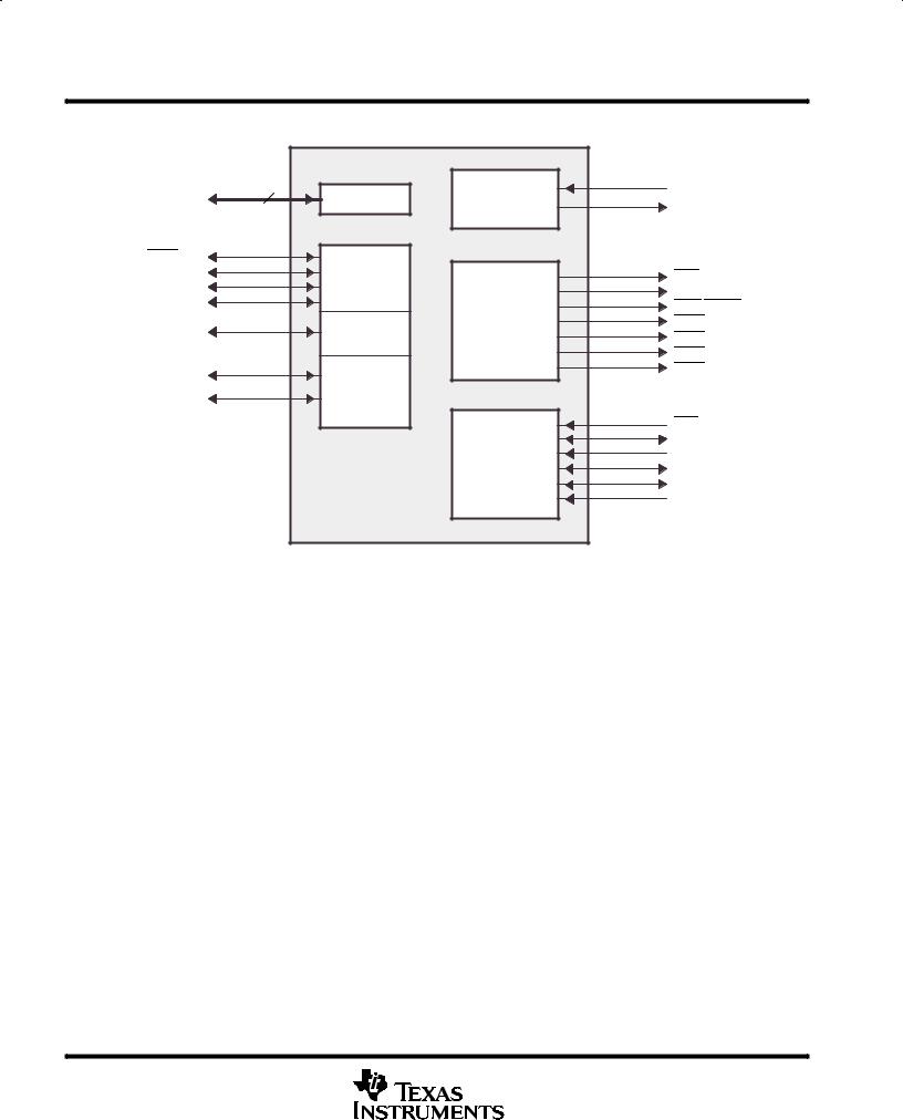
signal groups description
CLKIN |
|
|
|
CLKOUT2 |
|
|
|
CLKOUT1 |
|
|
|
CLKMODE0 |
|
|
RESET |
CLKMODE1 |
Clock/PLL |
|
NMI |
CLKMODE2† |
|
|
EXT_INT7 |
PLLV |
|
|
EXT_INT6 |
PLLG |
|
Reset and |
EXT_INT5 |
PLLF |
|
EXT_INT4 |
|
|
Interrupts |
||
|
|
|
IACK |
|
|
|
INUM3 |
TMS |
|
|
INUM2 |
|
|
INUM1 |
|
TDO |
IEEE Standard |
|
|
|
INUM0 |
||
TDI |
|
||
1149.1 |
|
|
|
TCK |
|
|
|
(JTAG) |
|
|
|
TRST |
|
|
|
Emulation |
|
|
|
EMU1 |
|
DMAC3 |
|
|
|
||
EMU0 |
|
DMA Status |
DMAC2 |
|
|
DMAC1 |
|
|
|
|
|
|
|
|
DMAC0 |
RSV4 |
|
|
|
RSV3 |
|
|
|
RSV2 |
Reserved |
Power-Down |
|
RSV1 |
|
PD |
|
|
Status |
||
RSV0 |
|
|
|
|
|
|
|
|
|
Control/Status |
|
† CLKMODE2 is NOT available on the GNZ package for the C6203B device.
Figure 2. CPU (DSP Core) Signals
20 |
POST OFFICE BOX 1443 • HOUSTON, TEXAS 77251–1443 |
TMS320C6203B
FIXED POINT DIGITAL SIGNAL PROCESSOR
SPRS086K – JANUARY 1999 – REVISED APRIL 2003
signal groups description (continued)
|
|
|
|
|
|
|
|
|
|
|
|
|
|
|
|
|
|
|
|
|
|
|
|
|
|
|
|
|
|
|
|
|
|
|
|
|
|
|
|
32 |
|
|
|
Asynchronous |
|
|
|
ARE |
|||||
ED[31:0] |
|
|
|
|
|
|
AOE |
||||||||||
|
Data |
|
|
|
|
||||||||||||
|
|
|
Memory |
|
|
|
AWE |
||||||||||
|
|
|
|
|
|
||||||||||||
|
|
|
|
|
|
|
|
Control |
|
|
|
||||||
|
|
|
|
|
|
|
|
|
|
|
ARDY |
||||||
|
|
|
|
|
|
|
|
|
|
|
|
|
|
|
|
|
|
CE3 |
|
|
|
|
|
|
|
|
|
|
|
|
|
|
|
||
|
|
|
|
|
|
|
|
|
|
|
|
|
|
|
|||
CE2 |
|
|
|
Memory Map |
|
|
|
|
|
|
|
|
|
|
|
||
CE1 |
|
|
|
|
Synchronous |
|
|
|
SDA10 |
|
|
||||||
|
|
|
Space Select |
|
|
|
|
||||||||||
CE0 |
|
|
|
|
|
|
|
SDRAS/SSOE |
|||||||||
|
|
|
|
|
Memory |
|
|
|
|||||||||
|
|
|
|
|
|
|
|
|
|
|
|
|
|
|
|
|
|
|
|
|
|
|
|
|
|
|
|
|
SDCAS/SSADS |
||||||
|
|
|
|
20 |
|
|
|
Control |
|
|
|
||||||
|
|
|
|
|
|
|
|
|
|
|
|
|
|
|
|
||
EA[21:2] |
|
|
Word Address |
|
|
|
|
SDWE/SSWE |
|||||||||
|
|
|
|
|
|
|
|
|
|
|
|
|
|
||||
|
|
|
|
|
|
|
|
|
|
|
|
|
|
|
|
|
|
|
BE3 |
|
|
|
|
|
|
HOLD/ |
|
|
|
HOLD |
|
|
|
|
|
|
|
|
|
|
|
|
|||||||||||
BE2 |
|
|
|
Byte Enables |
|
HOLDA |
|
|
|
HOLDA |
|
|
|
||||
BE1 |
|
|
|
|
|
|
|
|
|
|
|
|
|
|
|||
BE0 |
|
|
|
|
|
EMIF |
|
|
|
|
|
|
|
|
|||
|
|
|
|
|
|
|
|
|
|
|
|
|
|||||
|
|
|
|
|
|
|
(External Memory Interface) |
|
|
|
|
|
|
|
|
||
|
|
|
|
|
|
|
|
|
|
|
|
|
|
|
|
|
|
TOUT1 |
Timer 1 |
Timer 0 |
TOUT0 |
|
TINP1 |
TINP0 |
|||
|
|
|||
|
|
Timers |
|
|
|
McBSP1 |
McBSP0 |
|
|
CLKX1 |
Transmit |
|
CLKX0 |
|
FSX1 |
Transmit |
FSX0 |
||
DX1 |
|
|
DX0 |
|
CLKR1 |
|
|
CLKR0 |
|
FSR1 |
Receive |
Receive |
FSR0 |
|
DR1 |
|
|
DR0 |
|
CLKS1 |
Clock |
Clock |
CLKS0 |
|
|
|
McBSP2 |
|
|
|
|
Transmit |
CLKX2 |
|
|
|
FSX2 |
||
|
|
|
DX2 |
|
|
|
|
CLKR2 |
|
|
|
Receive |
FSR2 |
|
|
|
|
DR2 |
|
|
|
Clock |
CLKS2 |
|
|
|
McBSPs |
|
|
|
(Multichannel Buffered Serial Ports) |
|
||
Figure 3. Peripheral Signals
POST OFFICE BOX 1443 • HOUSTON, TEXAS 77251–1443 |
21 |
TMS320C6203B
FIXED POINT DIGITAL SIGNAL PROCESSOR
SPRS086K – JANUARY 1999 – REVISED APRIL 2003
signal groups description (continued)
XD[31:0] |
32 |
Clocks |
XCLKIN |
|
Data |
XFCLK |
|||
|
|
|
||
XBE3/XA5 |
Byte-Enable |
|
|
|
XBE2/XA4 |
|
XOE |
||
Control/ |
|
|||
XBE1/XA3 |
|
|||
|
XRE |
|||
Address |
|
|||
XBE0/XA2 |
|
|||
I/O Port |
XWE/XWAIT |
|||
|
||||
|
|
|||
XRDY |
Control |
Control |
XCE3 |
|
|
XCE2 |
|||
|
|
|
||
|
|
|
XCE1 |
|
XHOLD |
|
|
XCE0 |
|
|
|
|
||
XHOLDA |
Arbitration |
|
|
|
|
|
|
||
|
|
|
XCS |
|
|
|
Host |
XAS |
|
|
|
XCNTL |
||
|
|
Interface |
||
|
|
XW/R |
||
|
Expansion Bus |
Control |
||
|
XBLAST |
|||
|
|
|
||
|
|
|
XBOFF |
Figure 3. Peripheral Signals (Continued)
22 |
POST OFFICE BOX 1443 • HOUSTON, TEXAS 77251–1443 |