


|
TMS320TCI6618 |
|
|
|||||||||||||||||||||||
|
Communications Infrastructure KeyStone SoC |
|
|
|||||||||||||||||||||||
|
SPRS688—February 2011 |
www.ti.com |
||||||||||||||||||||||||
|
|
|
|
|
|
|
|
|
|
|
|
|
|
|
|
|
|
|
|
|
|
|
|
|||
|
Table 7-4 |
|
|
IO Before Core Power Sequencing |
|
|
||||||||||||||||||||
|
|
|
|
|
|
|
|
|
|
|
|
|
|
|
|
|
|
|
|
|
|
|
|
|
|
|
|
Time |
System State |
|
|
||||||||||||||||||||||
|
t1 |
Begin Power Stabilization Phase |
|
|
||||||||||||||||||||||
|
|
• DVDD18 (1.8 V) supply is ramped up followed coincidentally by HHV (1.8 V). |
|
|
||||||||||||||||||||||
|
|
• Because |
|
|
|
is low, all the core logic having async reset (created from POR) are put into reset state once the core supply ramps. |
|
must |
||||||||||||||||||
|
|
POR |
POR |
|||||||||||||||||||||||
|
|
|
|
remain low through Power Stabilization Phase. |
|
|
||||||||||||||||||||
|
|
• Filtered versions of 1.8 V can ramp simultaneously with DVDD18. |
|
|
||||||||||||||||||||||
|
|
• |
|
|
|
|
|
|
is driven low once the DVDD18 supply is available. |
|
|
|||||||||||||||
|
|
RESETSTAT |
|
|
||||||||||||||||||||||
|
|
• All input and bidirectional pins must not be driven or pulled high until DVDD18 is present. Driving an input or bidirectional pin before |
||||||||||||||||||||||||
|
|
|
|
DVDD18 could cause damage to the device. |
|
|
||||||||||||||||||||
|
|
|
|
|
|
|
|
|
||||||||||||||||||
|
t2a |
• |
|
|
|
may be driven high anytime after DVDD18 is at a valid level. |
|
|
||||||||||||||||||
|
RESET |
|
|
|||||||||||||||||||||||
ADVANCE |
t2b |
• CVDD (core AVS) ramps up. |
|
|
||||||||||||||||||||||
|
|
|
|
|
|
|
|
|
|
|
|
|
|
|
|
|
|
|
|
|
|
|
|
|
||
t3a |
• CVDD1 (core constant) ramps at the same time or following CVDD. Although ramping CVDD1 and CVDD simultaneously is permitted the |
|||||||||||||||||||||||||
|
||||||||||||||||||||||||||
|
|
|
|
voltage for CVDD1 must never exceed CVDD until after CVDD has reached a valid voltage. |
|
|
||||||||||||||||||||
|
|
• The purpose of ramping up the core supplies close to each other is to reduce crowbar current. CVDD1 should trail CVDD as this will ensure |
||||||||||||||||||||||||
|
|
|
|
that the WLs in the memories are turned off and there is no current through the memory bit cells. If, however, CVDD1 (core constant) |
||||||||||||||||||||||
|
|
|
|
ramps up before CVDD (core AVS), then the worst case current could be on the order of twice the specified draw of CVDD1. |
|
|
||||||||||||||||||||
|
|
|
||||||||||||||||||||||||
|
t3b |
• Once CVDD is valid, the clock drivers should be enabled. Although the clock inputs are not necessary at this time, they should either be |
||||||||||||||||||||||||
|
|
|
|
driven with a valid clock or held in a static state with one leg high and one leg low. |
|
|
||||||||||||||||||||
|
|
|
|
|
||||||||||||||||||||||
|
t3c |
• The DDRCLK and REFCLK may begin to toggle anytime between when CVDD is at a valid level and the setup time before |
|
goes high |
||||||||||||||||||||||
INFORMATION |
POR |
|||||||||||||||||||||||||
|
|
|
specified by t6. |
|
|
|||||||||||||||||||||
|
|
|
|
|
|
|||||||||||||||||||||
|
|
|
|
|
||||||||||||||||||||||
|
t4 |
• DVDD15 (1.5 V) supply is ramped up following CVDD1. |
|
|
||||||||||||||||||||||
|
|
|
|
|
|
|
|
|||||||||||||||||||
|
t5 |
• |
|
|
|
must continue to remain low for at least 100 μs after power has stabilized. |
|
|
||||||||||||||||||
|
POR |
|
|
|||||||||||||||||||||||
|
|
End Power Stabilization Phase |
|
|
||||||||||||||||||||||
|
|
|
|
|
||||||||||||||||||||||
|
t6 |
Begin Device Initialization |
|
|
||||||||||||||||||||||
|
|
• Device initialization requires 500 REFCLK periods after the Power Stabilization Phase. The maximum clock period is 33.33 nsec so a delay |
||||||||||||||||||||||||
|
|
|
|
of an additional 16 μs is required before a rising edge of POR. The clock must be active during the entire 16 μs. |
|
|
||||||||||||||||||||
|
|
• |
|
must remain low. |
|
|
||||||||||||||||||||
|
|
POR |
|
|
||||||||||||||||||||||
|
t7 |
• |
|
|
|
|
|
|
is held low for at least 24 transitions of the REFCLK after |
|
|
has stabilized at a high level. |
|
|
||||||||||||
|
RESETFULL |
POR |
|
|
||||||||||||||||||||||
|
|
• The rising edge of the |
|
will remove the reset to the efuse farm allowing the scan to begin. |
|
|
||||||||||||||||||||
|
|
RESETFULL |
|
|
||||||||||||||||||||||
|
t8 |
• Once device initialization and the efuse farm scan are complete, the |
|
|
signal is driven high. This delay will be 10000 to 50000 |
|||||||||||||||||||||
|
RESETSTAT |
|||||||||||||||||||||||||
|
|
|
|
clock cycles. |
|
|
||||||||||||||||||||
|
|
End Device Initialization Phase |
|
|
||||||||||||||||||||||
|
|
|
|
|
|
|
|
|
||||||||||||||||||
|
t9 |
• GPIO configuration bits must be valid for at least 12 transitions of the REFCLK before the rising edge of |
|
|
|
|
|
|
||||||||||||||||||
|
RESETFULL |
|
|
|||||||||||||||||||||||
|
t10 |
• GPIO configuration bits must be held valid for at least 12 transitions of the REFCLK after the rising edge of |
|
|
|
|
|
|||||||||||||||||||
|
RESETFULL |
|
|
|||||||||||||||||||||||
|
End of Table 7-4 |
|
|
|||||||||||||||||||||||
|
|
|
|
|
|
|
|
|
|
|
|
|
|
|
|
|
|
|
|
|
|
|
|
|
|
|
7.3.1.3 Prolonged Resets
Holding the device in POR, RESETFULL, or RESET for long periods of time will affect the long-term reliability of the part. The device should not be held in a reset for times exceeding one hour and should not be held in reset for more the 5% of the time during which power is applied. Exceeding these limits will cause a gradual reduction in the reliability of the part. This can be avoided by allowing the DSP to boot and then configuring it to enter a hibernation state soon after power is applied. This will satisfy the reset requirement while limiting the power consumption of the device.
7.3.2 Power-Down Sequence
The power down sequence is the exact reverse of the power-up sequence described above. The goal is to prevent a large amount of static current and to prevent overstress of the device. A power-good circuit that monitors all the supplies for the device should be used in all designs. If a catastrophic power supply failure occurs on any voltage rail, POR should transition to low to prevent over-current conditions that could possibly impact device reliability.
100 |
Copyright 2011 Texas Instruments Incorporated |
TMS320TCI6618
Communications Infrastructure KeyStone SoC
www.ti.com |
SPRS688—February 2011 |
|
A system power monitoring solution is needed to shut down power to the board if a power supply fails. Long-term exposure to an environment in which one of the power supply voltages is no longer present will affect the reliability of the device. Holding the device in reset is not an acceptable solution because prolonged periods of time with an active reset can also affect long term reliability.
Some of the clock inputs are required to be present for the device to initialize correctly, but behavior of many of the clocks is contingent on the state of the boot configuration pins. Table 7-5 describes the clock sequencing and the conditions that affect the clock operation. Note that all clock drivers should be in a high-impedance state until CVDD is at a valid level and that all clock inputs either be active or in a static state with one leg pulled low and the other connected to CVDD.
Table 7-5 |
Clock Sequencing |
|
|
|
|
|
|
|
|
|
|
|
|
|
|
|
|
|
|
|
|
|
|
|
|
|
|
|
|
|
|
|
|
Clock |
Condition |
Sequencing |
||||||||||||||
DDRCLK |
None |
Must be present 16 μsec before |
|
transitions high. |
||||||||||||
POR |
||||||||||||||||
|
CORECLKSEL = 0 |
SYSCLK used to clock the core PLL. It must be present 16 μsec before |
|
transitions high. |
||||||||||||
SYSCLK |
POR |
|||||||||||||||
CORECLKSEL = 1 |
SYSCLK used only for AIF. Clock most be present before the reset to the AIF is removed. |
|||||||||||||||
|
||||||||||||||||
|
|
|
||||||||||||||
ALTCORECLK |
CORECLKSEL = 0 |
ALTCORECLK is not used and should be tied to a static state. |
||||||||||||||
|
|
|
|
|
|
|
|
|
|
|
|
|
|
|
||
CORECLKSEL = 1 |
ALTCORECLK is used to clock the core PLL. It must be present 16 μsec before |
|
transitions high. |
|||||||||||||
|
POR |
|||||||||||||||
|
PASSCLKSEL = 0 |
PASSCLK is not used and should be tied to a static state. |
||||||||||||||
PASSCLK |
|
|
|
|
|
|
|
|
|
|
|
|
|
|
|
|
PASSCLKSEL = 1 |
PASSCLK is used as a source for the PA_SS PLL. It must be present before the PA_SS PLL is removed from |
|||||||||||||||
|
||||||||||||||||
|
|
reset and programmed. |
||||||||||||||
|
|
|
|
|
||||||||||||
|
An SGMII port will be used. |
SRIOSGMIICLK must be present 16 μsec before |
|
transitions high. |
||||||||||||
|
POR |
|||||||||||||||
|
SGMII will not be used. SRIO |
SRIOSGMIICLK must be present 16 μsec before |
|
|
transitions high. |
|||||||||||
|
POR |
|||||||||||||||
|
will be used as a boot device. |
|
|
|
|
|
|
|
|
|
|
|
|
|
|
|
SRIOSGMIICLK |
|
|
||||||||||||||
SGMII will not be used. SRIO |
SRIOSGMIICLK is used as a source to the SRIO SERDES PLL. It must be present before the SRIO is |
|||||||||||||||
|
will be used after boot. |
removed from reset and programmed. |
||||||||||||||
|
|
|
||||||||||||||
|
SGMII will not be used. SRIO |
SRIOSGMIICLK is not used and should be tied to a static state. |
||||||||||||||
|
will not be used. |
|
|
|
|
|
|
|
|
|
|
|
|
|
|
|
|
|
|
|
|
|
|||||||||||
|
PCIE will be used as a boot |
PCIECLK must be present 16 μsec before |
|
|
transitions high. |
|||||||||||
|
POR |
|||||||||||||||
|
device. |
|
|
|
|
|
|
|
|
|
|
|
|
|
|
|
PCIECLK |
|
|
||||||||||||||
PCIE will be used after boot. |
PCIECLK is used as a source to the PCIE SERDES PLL. It must be present before the PCIE is removed from |
|||||||||||||||
|
|
reset and programmed. |
||||||||||||||
|
|
|
||||||||||||||
|
PCIE will not be used. |
PCIECLK is not used and should be tied to a static state. |
||||||||||||||
|
|
|
|
|
||||||||||||
|
HyperLink will be used as a |
MCMCLK must be present 16 μsec before |
|
|
transitions high. |
|||||||||||
|
POR |
|||||||||||||||
|
boot device. |
|
|
|
|
|
|
|
|
|
|
|
|
|
|
|
|
|
|
||||||||||||||
MCMCLK |
HyperLink will be used after |
MCMCLK is used as a source to the HyperLink SERDES PLL. It must be present before the HyperLink is |
||||||||||||||
|
boot. |
removed from reset and programmed. |
||||||||||||||
|
|
|
||||||||||||||
|
HyperLink will not be used. |
MCMCLK is not used and should be tied to a static state. |
||||||||||||||
|
|
|
|
|
|
|
|
|
|
|
|
|
|
|
|
|
End of Table 7-5 |
|
|
|
|
|
|
|
|
|
|
|
|
|
|
||
|
|
|
|
|
|
|
|
|
|
|
|
|
|
|
|
|
7.3.3 Power Supply Decoupling and Bulk Capacitors
In order to properly decouple the supply planes on the PCB from system noise, decoupling and bulk capacitors are required. Bulk capacitors are used to minimize the effects of low frequency current transients and decoupling or bypass capacitors are used to minimize higher frequency noise. For recommendations on selection of Power Supply Decoupling and Bulk capacitors see the Hardware Design Guide for KeyStone Devices in ‘‘Related Documentation from Texas Instruments’’ on page 59.
ADVANCE INFORMATION
Copyright 2011 Texas Instruments Incorporated |
101 |
INFORMATION ADVANCE
TMS320TCI6618
Communications Infrastructure KeyStone SoC
SPRS688—February 2011 |
www.ti.com |
|
7.3.4 SmartReflex
Increasing the device complexity increases its power consumption and with the smaller transistor structures responsible for higher achievable clock rates and increased performance, comes an inevitable penalty, increasing the leakage currents. Leakage currents are present in any active circuit, independently of clock rates and usage scenarios. This static power consumption is mainly determined by transistor type and process technology. Higher clock rates also increase dynamic power, the power used when transistors switch. The dynamic power depends mainly on a specific usage scenario, clock rates, and I/O activity.
Texas Instruments' SmartReflex technology is used to decrease both static and dynamic power consumption while maintaining the device performance. SmartReflex in the TMS320TCI6618 device is a feature that allows the core voltage to be optimized based on the process corner of the device. This requires a voltage regulator for each TMS320TCI6618 device.
To guarantee maximizing performance and minimizing power consumption of the device, SmartReflex is required to be implemented whenever the TMS320TCI6618 device is used. The voltage selection is done using 4 VCNTL pins which are used to select the output voltage of the core voltage regulator.
For information on implementation of SmartReflex see the Power Management for KeyStone Devices application report and the Hardware Design Guide for KeyStone Devices in ‘‘Related Documentation from Texas Instruments’’ on page 59.
Table 7-6 |
SmartReflex 4-Pin VID Interface Switching Characteristics |
|
|
|
||
(see Figure 7-7) |
|
|
|
|
|
|
|
|
|
|
|
|
|
No. |
|
|
Parameter |
Min |
Max |
Unit |
1 |
td(Bn-SELECTL) |
Delay Time - VCNTL[2:0] (B[2:0]]) valid after VCNTL[3] (Select) low |
|
300.00 |
ns |
|
|
|
|
|
|
|
|
2 |
toh(SELECTL-Bn) |
Output Hold Time - VCNTL[2:0] (B[2:0]]) valid after VCNTL[3] (Select) low |
0.07 |
172020C (1) |
ms |
|
3 |
td(Bn-SELECTH) |
Delay Time - VCNTL[2:0] (B[2:0]]) valid after VCNTL[3] (Select) high |
|
300.00 |
ns |
|
|
|
|
|
|
|
|
4 |
toh(SELECTH-Bn) |
Output Hold Time - VCNTL[2:0] (B[2:0]]) valid after VCNTL[3] (Select) high |
0.07 |
172020C |
ms |
|
|
|
|
|
|
|
|
End of Table 7-6 |
|
|
|
|
|
|
|
|
|
|
|
||
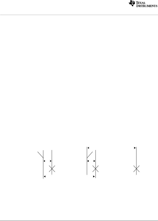
1 C = 1/REFCLK frequency (See Figure 7-19)in ms |
|
|
|
|||
Figure 7-7 |
SmartReflex 4-Pin VID Interface Timing |
|
|
|
|
|
|
|
|
|
|
|
|
|
|
|||||||||||||
|
|
|
|
|
|
|
|
|
|
|
|
|
|
|
|
|
|
|
|
|
|
|
|
|
|
|||
|
|
|
|
|
|
|
|
|
|
|
|
|
|
|
|
|
|
|
|
|
|
|
|
4 |
|
|
|
|
|
|
|
|
|
|
|
|
|
|
|
|
|
|
|
|
|
|
|
|
|
|
|
||||||
|
|
|
|
|
|
|
|
|
|
|
|
|
|
|
|
|
|
|
|
|
|
|
|
|
|
|
||
|
|
|
|
|
|
|
|
|
|
|
|
|
|
|
|
|
|
|
|
|
|
|
|
|
|
|
|
|
VCNTL[3] (Select) |
|
|
|
|
|
|
|
|
|
|
|
|
|
|
|
|
|
|
|
|
|
|
|
|
|
|||
|
|
|
|
|
|
|
|
|
|
|
|
|
|
|
|
|
|
|
|
|
|
|
|
|
|
|
|
|
|
|
|
|
|
|
|
|
|
|
|
|
|
|
|
|
|
|
|
|
|
|
|
|
|
|
|
|
|
|
|
|
|
|
|
|
1 |
|
|
|
|
|
|
|
|
|
3 |
|
|
|
|
|
|
|
|
|
|
|
|
|
|
|
|
|
|
|
|
|
|
|
|
|
|
|
|
|
|
|
|
|
|
|
|||||
|
|
|
|
|
|
|
|
|
|
|
|
|
|
|
|
|
|
|
|
|
|
|
|
|
|
|
|
|
VCNTL[2:0] (B[2:0]) |
|
|
|
|
|
|
|
|
LSB VID[2:0] |
|
|
|
|
|
|
|
|
MSB VID[5:3] |
||||||||||
|
|
|
|
|
|
|
|
|
|
|
|
|
|
|
|
|
|
|
|
|
|
|
|
|
|
|
|
|
|
|
|
|
|
|
|
|
|
|
|
|
|
|
|
|
|
|
|
|
|
|
|||||||
|
|
|
|
|
|
|
|
|
|
|
|
2 |
|
|
|
|
|
|
|
|
|
|
|
|
|
|
|
|
|
|
|
|
|
|
|
|
|
|
|
|
|
|
|
|
|
|
|
|
|||||||||
102 |
Copyright 2011 Texas Instruments Incorporated |