


TMS320TCI6618
Communications Infrastructure KeyStone SoC
SPRS688—February 2011 |
www.ti.com |
|
2 Device Overview
2.1 Device Characteristics
Table 2-1 provides an overview of the TMS320TCI6618 DSP. The table shows significant features of the TCI6618 device, including the capacity of on-chip RAM, the peripherals, the CPU frequency, and the package type with pin count.
2.2 CPU (DSP Core) Description
|
Table 2-1 |
Characteristics of the TCI6618 Processor (Part 1 of 2) |
|
|
ADVANCE |
|
|
HARDWARE FEATURES |
TMS320TCI6618 |
|
|
DDR3 Memory Controller (64-bit bus width) [1.5 V I/O] |
1 |
|
|
|
|
||
|
|
|
(clock source = DDRREFCLKN|P) |
|
|
|
|
|
|
|
|
|
EDMA3 (16 independent channels) [CPU/2 clock rate] |
1 |
|
|
|
|
|
|
|
|
EDMA3 (64 independent channels) [CPU/3 clock rate] |
2 |
|
|
|
|
|
|
|
|
High-speed 1×/2x/4× Serial RapidIO Port (4 lanes) |
1 |
|
|
|
|
|
|
|
|
Second generation Antenna Interface (AIF2) |
1 |
|
|
|
|
|
|
|
|
2 |
1 |
INFORMATION |
|
|
I C |
|
Peripherals |
|
SPI |
1 |
|
|
|
|||
|
|
|
|
|
|
|
|
PCIe (2 lanes) |
1 |
|
|
|
|
|
|
|
|
UART |
1 |
|
|
|
|
|
|
|
|
10/100/1000 Ethernet MAC (EMAC) |
2 |
|
|
|
|
|
|
|
|
Management Data Input/Output (MDIO) |
1 |
|
|
|
|
|
|
|
|
64-Bit Timers (Configurable) |
Eight 64-bit or Sixteen 32-bit |
|
|
|
(internal clock source = CPU/6 clock frequency) |
|
|
|
|
|
|
|
|
|
|
|
|
|
|
General-Purpose Input/Output Port (GPIO) |
16 |
|
|
|
|
|
|
|
|
VCP2 (clock source = CPU/3 clock frequency) |
4 |
|
|
|
|
|
|
|
|
TCP3d (clock source = CPU/2 clock frequency) |
3 |
|
Encoder/Decoder |
|
|
|
|
TCP3e (clock source = CPU/3 clock frequency) |
1 |
||
|
Coprocessors |
|
||
|
|
|
|
|
|
|
FFTC (clock source = CPU/3 clock frequency) |
3 |
|
|
|
|
||
|
|
|
|
|
|
|
|
BCP (clock source = CPU/3 clock frequency) |
1 |
|
|
|
|
|
|
|
|
Receive Accelerator (RAC) |
2 |
|
|
|
|
|
|
|
|
Transmit Accelerator (TAC) |
1 |
|
|
|
|
|
|
Accelerators |
|
Rake/Search Accelerator |
4 |
|
|
|
|
|
|
|
|
Packet Accelerator |
1 |
|
|
|
|
|
|
|
|
Security Accelerator (1) |
1 |
|
|
|
Size (Bytes) |
6528K |
|
|
|
|
|
|
|
|
|
128KB L1 Program Memory Controller |
|
On-Chip Memory |
|
[SRAM/Cache] 128KB L1 Data Memory Controller |
|
|
Organization |
[SRAM/Cache] 4096KB L2 Unified Memory/Cache |
||
|
|
|
||
|
|
|
|
2048KB MSM SRAM |
|
|
|
|
128KB L3 ROM |
|
|
|
|
|
|
C66x CorePac |
|
CorePac Revision ID Register (address location: 0181 2000h) |
See Section 5.6 ‘‘CorePac Revision’’ on page 88. |
|
Revision ID |
|
||
|
|
|
|
|
|
|
|
|
|
|
JTAG BSDL_ID |
|
JTAGID register (address location: 0x02620018) |
See Section 3.3.3 ‘‘JTAG ID (JTAGID) Register |
|
|
Description’’ on page 65 |
||
|
|
|
|
|
|
|
|
|
|
|
Frequency |
|
MHz |
1200 (1.2 GHz) [-1200] |
|
|
|
|
1000 (1.0 GHz) [-1000] |
|
|
|
|
|
|
|
|
|
|
|
14 |
|
|
Copyright 2011 Texas Instruments Incorporated |

|
|
|
|
TMS320TCI6618 |
|
|
|
Communications Infrastructure KeyStone SoC |
|
www.ti.com |
|
|
|
SPRS688—February 2011 |
|
|
|
|
|
Table 2-1 |
Characteristics of the TCI6618 Processor (Part 2 of 2) |
|||
|
|
|
|
|
|
|
HARDWARE FEATURES |
|
TMS320TCI6618 |
Cycle Time |
|
ns |
|
0.83 ns [-1200] |
|
|
|
|
1 ns [-1000] |
|
|
|
|
|
Voltage |
|
Core (V) |
|
SmartReflex variable supply |
|
|
|
|
|
|
I/O (V) |
|
1.0 V, 1.5 V, and 1.8 V |
|
|
|
|
||
|
|
|
|
|
BGA Package |
|
24 mm × 24 mm |
|
841-Pin Flip-Chip Plastic BGA (CYP) |
|
|
|
|
|
Process Technology |
μm |
|
0.040 μm |
|
|
|
|
|
|
Product Status (2) |
|
Product Preview (PP), Advance Information (AI), |
|
AI |
|
|
or Production Data (PD) |
|
|
End of Table 2-1 |
|
|
|
|
|
|
|
|
|
1 The Security Accelerator function is subject to export control and will be enabled only for approved device shipments.
2 ADVANCE INFORMATION concerns new products in the sampling or preproduction phase of development. Characteristic data and other specifications are subject to change without notice.
The C66x Central Processing Unit (CPU) extends the performance of the C64x+ and C674x CPUs through enhancements and new features. Many of the new features target increased performance for vector processing. The C64x+ and C674x CPUs support 2-way SIMD operations for 16-bit data and 4-way SIMD operations for 8-bit data. On the C66x CPU, the vector processing capability is improved by extending the width of the SIMD instructions. C66x CPUs can execute instructions that operate on 128-bit vectors. For example the QMPY32 instruction is able to perform the element-to-element multiplication between two vectors of four 32-bit data each. The C66x CPU also supports SIMD for floating-point operations. Improved vector processing capability (each instruction can process multiple data in parallel) combined with the natural instruction level parallelism of C6000 architecture (e.g execution of up to 8 instructions per cycle) results in a very high level of parallelism that can be exploited by DSP programmers through the use of TI's optimized C/C++ compiler.
The C66x CPU consists of eight functional units, two register files, and two data paths as shown in Figure 2-1. The two general-purpose register files (A and B) each contain 32 32-bit registers for a total of 64 registers. The general-purpose registers can be used for data or can be data address pointers. The data types supported include packed 8-bit data, packed 16-bit data, 32-bit data, 40-bit data, and 64-bit data. Multiplies also support 128-bit data. 40-bit-long or 64-bit-long values are stored in register pairs, with the 32 LSBs of data placed in an even register and the remaining 8 or 32 MSBs in the next upper register (which is always an odd-numbered register). 128-bit data values are stored in register quadruplets, with the 32 LSBs of data placed in a register that is a multiple of 4 and the remaining 96 MSBs in the next 3 upper registers.
The eight functional units (.M1, .L1, .D1, .S1, .M2, .L2, .D2, and .S2) are each capable of executing one instruction every clock cycle. The .M functional units perform all multiply operations. The .S and .L units perform a general set of arithmetic, logical, and branch functions. The .D units primarily load data from memory to the register file and store results from the register file into memory.
Each C66x .M unit can perform one of the following fixed-point operations each clock cycle: four 32 × 32 bit multiplies, sixteen 16 × 16 bit multiplies, four 16 × 32 bit multiplies, four 8 × 8 bit multiplies, four 8 × 8 bit multiplies with add operations, and four 16 × 16 multiplies with add/subtract capabilities. There is also support for Galois field multiplication for 8-bit and 32-bit data. Many communications algorithms such as FFTs and modems require complex multiplication. Each C66x .M unit can perform one 16 × 16 bit complex multiply with or without rounding capabilities, two 16 × 16 bit complex multiplies with rounding capability, and a 32 × 32 bit complex multiply with rounding capability. The C66x can also perform two 16 × 16 bit and one 32 × 32 bit complex multiply instructions that multiply a complex number with a complex conjugate of another number with rounding capability. Communication signal processing also requires an extensive use of matrix operations. Each C66x .M unit is capable of multiplying a [1 × 2] complex vector by a [2 × 2] complex matrix per cycle with or without rounding capability. A version also exists allowing multiplication of the conjugate of a [1 × 2] vector with a [2 × 2] complex matrix.
Copyright 2011 Texas Instruments Incorporated |
15 |
ADVANCE INFORMATION

INFORMATION ADVANCE
TMS320TCI6618
Communications Infrastructure KeyStone SoC
SPRS688—February 2011 |
www.ti.com |
|
Each C66x .M unit also includes IEEE floating-point multiplication operations from the C674x CPU. This includes one single-precision multiply each cycle and one double precision multiply every 4 cycles. There is also a mixed-precision multiply that allows multiplication of a single-precision value by a double-precision value and an operation allowing multiplication of two single-precision numbers resulting in a double-precision number. The C66x CPU improves the performance over the C674x double-precision multiplies by adding a instruction allowing one double-precision multiply per cycle and also reduces the number of delay slots from 10 down to 4. Each C66x
.M unit can also perform one the following floating-point operations each clock cycle: one, two, or four single-precision multiplies or a complex single-precision multiply.
The .L and .S units can now support up to 64-bit operands. This allows for new versions of many of the arithmetic, logical, and data packing instructions to allow for more parallel operations per cycle. Additional instructions were added yielding performance enhancements of the floating point addition and subtraction instructions, including the ability to perform one double precision addition or subtraction per cycle. Conversion to/from integer and single-precision values can now be done on both .L and .S units on the C66x. Also, by taking advantage of the larger operands, instructions were also added to double the number of these conversions that can be done. The .L unit also has additional instructions for logical AND and OR instructions, as well as, 90 degree or 270 degree rotation of complex numbers (up to two per cycle). Instructions have also been added that allow for the computing the conjugate of a complex number.
The MFENCE instruction is a new instruction introduced on the C66x DSP. This instruction will create a CPU stall until the completion of all the CPU-triggered memory transactions, including:
•Cache line fills
•Writes from L1D to L2 or from the CorePac to MSMC and/or other system endpoints
•Victim write backs
•Block or global coherence operations
•Cache mode changes
•Outstanding XMC prefetch requests
This is useful as a simple mechanism for programs to wait for these requests to reach their endpoint. It also provides ordering guarantees for writes arriving at a single endpoint via multiple paths, multiprocessor algorithms that depend on ordering, and manual coherence operations.
For more details on the C66x CPU and its enhancements over the C64x+ and C674x architectures, see the following documents ( ‘‘Related Documentation from Texas Instruments’’ on page 59):
•C66x CPU and Instruction Set Reference Guide
•C66x DSP Cache User Guide
•C66x CorePac User Guide
16 |
Copyright 2011 Texas Instruments Incorporated |
TMS320TCI6618
Communications Infrastructure KeyStone SoC
www.ti.com |
SPRS688—February 2011 |
|
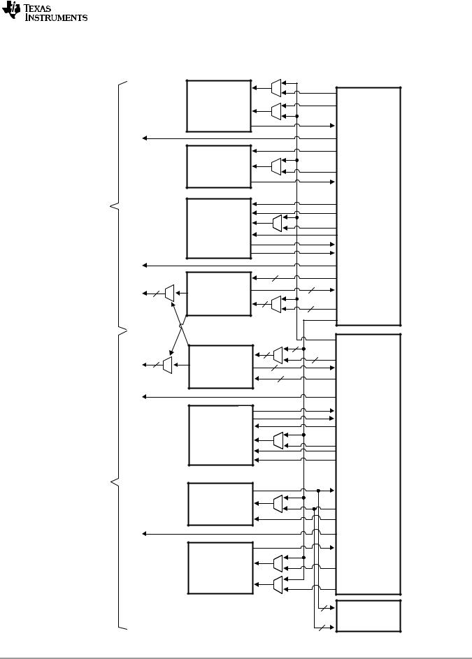
Figure 2-1 shows the DSP core functional units and data paths.
Figure 2-1 TMS320TCI6618 CPU (DSP Core) Data Paths
Note: |
|
src1 |
|
|
|
Default bus width |
|
|
|
|
|
|
|
|
|
|
|
is 64 bits |
|
|
|
|
|
(i.e. a register pair) |
.L1 |
src2 |
|
|
Register |
|
|
|
|
File A |
|
|
|
|
|
|
|
|
|
dst |
|
|
(A0, A1, A2, |
ST1 |
|
|
|
|
...A31) |
|
|
|
|
|
|
|
|
src1 |
|
|
|
|
.S1 |
src2 |
|
|
|
|
|
dst |
|
|
|
Data Path A |
|
src1 |
|
|
|
|
src1_hi |
|
|
|
|
|
|
|
|
|
|
|
.M1 |
src2 |
|
|
|
|
src2_hi |
|
|
|
|
|
|
|
|
|
|
|
|
dst2 |
|
|
|
|
|
dst1 |
|
|
|
LD1 |
|
|
|
|
|
|
|
src1 |
32 |
|
|
|
|
|
|
|
|
DA1 |
.D1 |
dst |
|
32 |
|
|
|
|
|||
32 |
|
|
|
|
|
|
|
src2 |
|
|
|
|
|
|
32 |
32 |
|
|
|
|
|
|
|
|
|
|
|
|
2 |
|
|
|
|
|
1 |
|
|
src2 |
32 |
|
Register |
|
|
32 |
|
File B |
|
DA2 |
.D2 |
|
32 |
||
dst |
|
(B0, B1, B2, |
|||
32 |
32 |
|
|||
|
|
|
|
|
|
|
|
src1 |
32 |
|
...B31) |
|
|
|
|
|
|
LD2 |
|
|
|
|
|
|
|
dst1 |
|
|
|
|
|
dst2 |
|
|
|
|
|
src2_hi |
|
|
|
|
.M2 |
src2 |
|
|
|
|
|
|
|
|
|
|
|
src1_hi |
|
|
|
|
|
src1 |
|
|
|
Data Path B |
|
|
|
|
|
|
|
dst |
|
|
|
|
.S2 |
src2 |
|
|
|
|
|
src1 |
|
|
|
ST2 |
|
|
|
|
|
|
|
dst |
|
|
|
|
.L2 |
src2 |
|
|
|
|
|
|
|
|
|
|
|
src1 |
|
|
|
|
|
|
|
32 |
Control |
|
|
|
|
|
Register |
66xx |
|
|
|
32 |
|
ADVANCE INFORMATION
Copyright 2011 Texas Instruments Incorporated |
17 |