


|
TMS320TCI6618 |
|
|
|
|
|
||
|
Communications Infrastructure KeyStone SoC |
|
|
|||||
|
SPRS688—February 2011 |
|
|
|
www.ti.com |
|
||
|
|
|
|
|
|
|
|
|
|
Table 7-17 |
INTC2 Registers (Part 2 of 2) |
|
|
|
|
||
|
|
|
|
|
|
|
|
|
|
Address Offset |
|
Register Mnemonic |
|
|
Register Name |
|
|
|
0x41c |
|
CH_MAP_REG7 |
|
|
Interrupt Channel Map Register for 28 to 28+3 |
|
|
|
|
|
|
|
|
|
|
|
|
0x420 |
|
CH_MAP_REG8 |
|
|
Interrupt Channel Map Register for 32 to 32+3 |
|
|
|
|
|
|
|
|
|
|
|
|
0x424 |
|
CH_MAP_REG9 |
|
|
Interrupt Channel Map Register for 36 to 36+3 |
|
|
|
|
|
|
|
|
|
|
|
|
0x428 |
|
CH_MAP_REG10 |
|
|
Interrupt Channel Map Register for 40 to 40+3 |
|
|
|
|
|
|
|
|
|
|
|
|
0x42c |
|
CH_MAP_REG11 |
|
|
Interrupt Channel Map Register for 44 to 44+3 |
|
|
|
|
|
|
|
|
|
|
|
|
0x430 |
|
CH_MAP_REG12 |
|
|
Interrupt Channel Map Register for 48 to 48+3 |
|
|
|
|
|
|
|
|
|
|
|
|
0x434 |
|
CH_MAP_REG13 |
|
|
Interrupt Channel Map Register for 52 to 52+3 |
|
|
|
|
|
|
|
|
|
|
|
ADVANCE |
0x438 |
|
CH_MAP_REG14 |
|
|
Interrupt Channel Map Register for 56 to 56+3 |
|
|
|
|
|
|
|
|
|
|
|
0x43c |
|
CH_MAP_REG15 |
|
|
Interrupt Channel Map Register for 60 to 60+3 |
|
||
|
|
|
|
|
||||
|
|
|
|
|
|
|
|
|
|
0x800 |
|
HINT_MAP_REG0 |
|
|
Host Interrupt Map Register for 0 to 0+3 |
|
|
|
|
|
|
|
|
|
|
|
|
0x804 |
|
HINT_MAP_REG1 |
|
|
Host Interrupt Map Register for 4 to 4+3 |
|
|
|
|
|
|
|
|
|
|
|
|
0x808 |
|
HINT_MAP_REG2 |
|
|
Host Interrupt Map Register for 8 to 8+3 |
|
|
|
|
|
|
|
|
|
|
|
|
0x80c |
|
HINT_MAP_REG3 |
|
|
Host Interrupt Map Register for 12 to 12+3 |
|
|
|
|
|
|
|
|
|
|
|
|
0x810 |
|
HINT_MAP_REG4 |
|
|
Host Interrupt Map Register for 16 to 16+3 |
|
|
INFORMATION |
|
|
|
|
|
|
|
|
0x814 |
|
HINT_MAP_REG5 |
|
|
Host Interrupt Map Register for 20 to 20+3 |
|
||
|
|
|
|
|
|
|
|
|
0x818 |
|
HINT_MAP_REG6 |
|
|
Host Interrupt Map Register for 24 to 24+3 |
|
||
|
|
|
|
|
||||
|
|
|
|
|
|
|
|
|
|
0x81c |
|
HINT_MAP_REG7 |
|
|
Host Interrupt Map Register for 28 to 28+3 |
|
|
|
|
|
|
|
|
|
|
|
|
0x820 |
|
HINT_MAP_REG8 |
|
|
Host Interrupt Map Register for 32 to 32+3 |
|
|
|
|
|
|
|
|
|
|
|
|
0x824 |
|
HINT_MAP_REG9 |
|
|
Host Interrupt Map Register for 36 to 36+3 |
|
|
|
|
|
|
|
|
|
|
|
|
0x828 |
|
HINT_MAP_REG10 |
|
|
Host Interrupt Map Register for 40 to 40+3 |
|
|
|
|
|
|
|
|
|
|
|
|
0x1500 |
|
ENABLE_HINT_REG0 |
|
|
Host Int Enable Register 0 |
|
|
|
|
|
|
|
|
|
|
|
|
0x1504 |
|
ENABLE_HINT_REG1 |
|
|
Host Int Enable Register 1 |
|
|
|
|
|
|
|
|
|
|
|
|
End of Table 7-17 |
|
|
|
|
|
||
|
|
|
|
|
|
|
|
|
|
7.5.3 Inter-Processor Register Map |
|
|
|
|
|||
|
Table 7-18 |
IPC Generation Registers (IPCGRx) (Part 1 of 2) |
|
|
||||
|
|
|
|
|
|
|
|
|
|
Address Start |
|
Address End |
Size |
Register Name |
Description |
|
|
|
0x02620200 |
|
0x02620203 |
4B |
NMIGR0 |
NMI Event Generation Register for Core 0 |
|
|
|
|
|
|
|
|
|
|
|
|
0x02620204 |
|
0x02620207 |
4B |
NMIGR1 |
NMI Event Generation Register for Core 1 |
|
|
|
|
|
|
|
|
|
|
|
|
0x02620208 |
|
0x0262020B |
4B |
NMIGR2 |
NMI Event Generation Register for Core 2 |
|
|
|
|
|
|
|
|
|
|
|
|
0x0262020C |
|
0x0262020F |
4B |
NMIGR3 |
NMI Event Generation Register for Core 3 |
|
|
|
|
|
|
|
|
|
|
|
|
0x02620210 |
|
0x02620213 |
4B |
Reserved |
Reserved |
|
|
|
|
|
|
|
|
|
|
|
|
0x02620214 |
|
0x02620217 |
4B |
Reserved |
Reserved |
|
|
|
|
|
|
|
|
|
|
|
|
0x02620218 |
|
0x0262021B |
4B |
Reserved |
Reserved |
|
|
|
|
|
|
|
|
|
|
|
|
0x0262021C |
|
0x0262021F |
4B |
Reserved |
Reserved |
|
|
|
|
|
|
|
|
|
|
|
|
0x02620220 |
|
0x0262023F |
32B |
Reserved |
Reserved |
|
|
|
|
|
|
|
|
|
|
|
|
0x02620240 |
|
0x02620243 |
4B |
IPCGR0 |
IPC Generation Register for Core 0 |
|
|
|
|
|
|
|
|
|
|
|
|
0x02620244 |
|
0x02620247 |
4B |
IPCGR1 |
IPC Generation Register for Core 1 |
|
|
|
|
|
|
|
|
|
|
|
|
0x02620248 |
|
0x0262024B |
4B |
IPCGR2 |
IPC Generation Register for Core 2 |
|
|
|
|
|
|
|
|
|
|
|
|
0x0262024C |
|
0x0262024F |
4B |
IPCGR3 |
IPC Generation Register for Core 3 |
|
|
|
|
|
|
|
|
|
|
|
|
0x02620250 |
|
0x02620253 |
4B |
Reserved |
Reserved |
|
|
|
|
|
|
|
|
|
|
|
|
0x02620254 |
|
0x02620257 |
4B |
Reserved |
Reserved |
|
|
|
|
|
|
|
|
|
|
|
|
|
|
|
|
|
|
|
|
|
130 |
|
|
|
|
|
Copyright 2011 Texas Instruments Incorporated |
|
|
|
|
|
|
|
TMS320TCI6618 |
|
|
|
|
|
Communications Infrastructure KeyStone SoC |
|
www.ti.com |
|
|
|
|
|
SPRS688—February 2011 |
|
|
|
|
|
|
|
Table 7-18 |
IPC Generation Registers (IPCGRx) (Part 2 of 2) |
|
|
|||
|
|
|
|
|
|
|
Address Start |
|
Address End |
Size |
Register Name |
|
Description |
0x02620258 |
|
0x0262025B |
4B |
Reserved |
|
Reserved |
|
|
|
|
|
|
|
0x0262025C |
|
0x0262025F |
4B |
Reserved |
|
Reserved |
|
|
|
|
|
|
|
0x02620260 |
|
0x0262027B |
28B |
Reserved |
|
Reserved |
|
|
|
|
|
|
|
0x0262027C |
|
0x0262027F |
4B |
IPCGRH |
|
IPC Generation Register for Host |
|
|
|
|
|
|
|
0x02620280 |
|
0x02620283 |
4B |
IPCAR0 |
|
IPC Acknowledgement Register for Core 0 |
|
|
|
|
|
|
|
0x02620284 |
|
0x02620287 |
4B |
IPCAR1 |
|
IPC Acknowledgement Register for Core 1 |
|
|
|
|
|
|
|
0x02620288 |
|
0x0262028B |
4B |
IPCAR2 |
|
IPC Acknowledgement Register for Core 2 |
|
|
|
|
|
|
|
0x0262028C |
|
0x0262028F |
4B |
IPCAR3 |
|
IPC Acknowledgement Register for Core 3 |
|
|
|
|
|
|
|
0x02620290 |
|
0x02620293 |
4B |
Reserved |
|
Reserved |
|
|
|
|
|
|
|
0x02620294 |
|
0x02620297 |
4B |
Reserved |
|
Reserved |
|
|
|
|
|
|
|
0x02620298 |
|
0x0262029B |
4B |
Reserved |
|
Reserved |
|
|
|
|
|
|
|
0x0262029C |
|
0x0262029F |
4B |
Reserved |
|
Reserved |
|
|
|
|
|
|
|
0x026202A0 |
|
0x026202BB |
28B |
Reserved |
|
Reserved |
|
|
|
|
|
|
|
0x026202BC |
|
0x026202BF |
4B |
IPCARH |
|
IPC Acknowledgement Register for Host |
|
|
|
|
|
|
|
End of Table 7-18 |
|
|
|
|
||
|
|
|
|
|
|
|
7.5.4 NMI and LRESET
The Non-Maskable Interrupts (NMI) can be generated by chip-level registers and the LRESET can be generated by software writing into LPSC registers. LRESET and NMI can also be asserted by device pins or Watch Dog Timers. One NMI pin and one LRESET pin are shared by all four CorePacs on the device. The CORESEL[2:0] pins can be configured to select between the four CorePacs available as shown in Table 7-19.
Table 7-19 LRESET and NMI Decoding
|
|
|
|
|
|
|
|
|
|
|
|
|
|
|
|
|
|
|
CORESEL[2:0] Pin Input |
|
LRESET Pin Input |
|
NMI Pin Input |
|
LRESETNMIEN Pin Input |
Reset Mux Block Output |
|||||||||||
XXX |
X |
X |
1 |
|
No local reset or |
|
assertion |
|||||||||||
|
NMI |
|||||||||||||||||
000 |
0 |
|
|
X |
0 |
|
Assert local reset to CorePac 0 |
|||||||||||
|
|
|
|
|
|
|
|
|||||||||||
001 |
0 |
|
|
X |
0 |
|
Assert local reset to CorePac 1 |
|||||||||||
|
|
|
|
|
|
|
|
|||||||||||
010 |
0 |
|
|
X |
0 |
|
Assert local reset to CorePac 2 |
|||||||||||
|
|
|
|
|
|
|
|
|||||||||||
011 |
0 |
|
|
X |
0 |
|
Assert local reset to CorePac 3. |
|||||||||||
|
|
|
|
|
|
|
||||||||||||
1xx |
0 |
|
X |
0 |
|
Assert local reset to all CorePac s |
||||||||||||
|
|
|
|
|
|
|
|
|
|
|||||||||
000 |
1 |
|
1 |
|
0 |
|
De-assert local reset & |
|
to CorePac 0 |
|||||||||
|
|
|
NMI |
|||||||||||||||
001 |
1 |
|
1 |
|
0 |
|
De-assert local reset & |
|
|
to CorePac 1 |
||||||||
|
|
|
NMI |
|||||||||||||||
010 |
1 |
|
1 |
|
0 |
|
De-assert local reset & |
|
|
to CorePac 2 |
||||||||
|
|
|
NMI |
|||||||||||||||
011 |
1 |
|
1 |
|
0 |
|
De-assert local reset & |
|
|
to CorePac 3 |
||||||||
|
|
|
NMI |
|||||||||||||||
1xx |
1 |
|
1 |
|
0 |
|
De-assert local reset & |
|
|
to all CorePac s |
||||||||
|
|
|
NMI |
|||||||||||||||
000 |
1 |
|
0 |
|
0 |
|
Assert |
|
to CorePac 0 |
|||||||||
|
|
|
NMI |
|||||||||||||||
001 |
1 |
|
0 |
|
0 |
|
Assert |
|
|
to CorePac 1 |
||||||||
|
|
|
NMI |
|||||||||||||||
010 |
1 |
|
0 |
|
0 |
|
Assert |
|
|
to CorePac 2 |
||||||||
|
|
|
NMI |
|||||||||||||||
011 |
1 |
|
0 |
|
0 |
|
Assert |
|
|
to CorePac 3 |
||||||||
|
|
|
NMI |
|||||||||||||||
1xx |
1 |
|
0 |
|
0 |
|
Assert |
|
|
to all CorePac s |
||||||||
|
|
|
NMI |
|||||||||||||||
End of Table 7-19 |
|
|
|
|
|
|
|
|
|
|
|
|
|
|
|
|
|
|
|
|
|
|
|
|
|
|
|
|
|
|
|
|
|
|
|
|
|
ADVANCE INFORMATION
Copyright 2011 Texas Instruments Incorporated |
131 |
INFORMATION ADVANCE
TMS320TCI6618 |
|
|
|
|
|
|
|
|
|
|
|
|
|
|
|
|
|
|
|
|
|
|
|
|
|
||||||||||||||||||||||||
Communications Infrastructure KeyStone SoC |
|
|
|
||||||||||||||||||||||||||||||||||||||||||||||
SPRS688—February 2011 |
|
|
|
|
|
|
|
|
|
|
|
|
|
|
|
|
|
|
|
|
|
|
|
|
www.ti.com |
||||||||||||||||||||||||
|
|
|
|
|
|
|
|
|
|
|
|
|
|
|
|
|
|
|
|
|
|
|
|
|
|
|
|
|
|
|
|
|
|
|
|
|
|
|
|
|
|
|
|
|
|
|
|
|
|
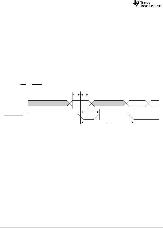
7.5.5 External Interrupts Electrical Data/Timing |
|
|
|
||||||||||||||||||||||||||||||||||||||||||||||
Table 7-20 |
|
|
|
|
and |
|
|
|
|
|
Timing Requirements (1) |
|
|
|
|||||||||||||||||||||||||||||||||||
NMI |
LRESET |
|
|
|
|||||||||||||||||||||||||||||||||||||||||||||
(see Figure 7-9) |
|
|
|
|
|
|
|
|
|
|
|
|
|
|
|
|
|
|
|
|
|
|
|
|
|
|
|
|
|
|
|
|
|
|
|
|
|
|
|
|
|
|
|||||||
|
|
|
|
|
|
|
|
|
|
|
|
|
|
|
|
|
|
|
|
|
|
|
|
|
|
|
|
|
|
|
|
|
|
|
|
|
|
|
|
|
|
|
|
|
|
|
|
|
|
No. |
|
|
|
|
|
|
|
|
|
|
|
|
|
|
|
|
|
|
|
|
|
|
|
|
|
|
|
|
|
|
|
|
|
|
|
|
|
|
|
|
|
|
|
|
|
|
Min |
Max |
Unit |
1 |
|
|
|
|
|
|
|
|
- |
|
|
|
|
|
|
|
|
|
|
|
|
|
|
Setup Time - |
|
|
|
|
|
valid before |
|
|
|
|
|
|
low |
TBD |
|
μs |
|||||||||
tsu(LRESET |
LRESETNMIENL) |
LRESET |
LRESETNMIEN |
|
|||||||||||||||||||||||||||||||||||||||||||||
1 |
|
|
|
|
|
|
|
|
|
|
|
|
|
|
|
|
|
|
|
|
|
|
|
|
|
|
|
|
|
|
|
|
|
|
|
|
|
|
|
|
|
|
|
|
|
|
TBD |
|
μs |
tsu(NMI |
-LRESETNMIENL) |
Setup Time - NMI valid before LRESETNMIEN low |
|
||||||||||||||||||||||||||||||||||||||||||||||
1 |
tsu(CORESELn- |
|
|
|
|
|
|
|
|
|
|
|
|
|
Setup Time - CORESEL[2:0] valid before |
|
|
|
|
|
|
low |
TBD |
|
μs |
||||||||||||||||||||||||
LRESETNMIENL) |
LRESETNMIEN |
|
|||||||||||||||||||||||||||||||||||||||||||||||
2 |
|
|
|
|
|
|
|
|
|
|
|
|
|
- |
|
|
|
|
|
|
Hold Time - |
|
|
|
|
|
valid after |
|
|
|
|
|
|
low |
TBD |
|
μs |
||||||||||||
th(LRESETNMIENL |
LRESET) |
LRESET |
LRESETNMIEN |
|
|||||||||||||||||||||||||||||||||||||||||||||
2 |
|
|
|
|
|
|
|
|
|
|
|
|
|
- |
|
|
|
|
Hold Time - |
|
|
|
valid after |
|
|
|
|
|
|
|
|
low |
TBD |
|
μs |
||||||||||||||
th(LRESETNMIENL |
NMI) |
NMI |
LRESETNMIEN |
|
|||||||||||||||||||||||||||||||||||||||||||||
2 |
|
|
|
|
|
|
|
|
|
|
|
|
|
|
-CORESELn) |
Hold Time - CORESEL[2:0] valid after |
|
|
|
|
|
|
low |
TBD |
|
μs |
|||||||||||||||||||||||
th(LRESETNMIENL |
LRESETNMIEN |
|
|||||||||||||||||||||||||||||||||||||||||||||||
3 |
|
|
|
|
|
|
|
|
|
|
|
|
|
|
|
|
Pulse Width - |
|
|
|
|
|
|
|
low width |
TBD |
|
μs |
|||||||||||||||||||||
tw(LRESETNMIEN) |
LRESETNMIEN |
|
|||||||||||||||||||||||||||||||||||||||||||||||
4 |
|
|
|
|
|
|
|
|
|
|
|
|
- |
|
|
|
|
|
|
|
|
|
Cycle Time - time between |
|
|
|
|
|
|
|
|
low |
TBD |
|
μs |
||||||||||||||
tc(LRESETNMIENL |
LRESETNMIENL) |
LRESETNMIEN |
|
||||||||||||||||||||||||||||||||||||||||||||||
End of Table 7-20 |
|
|
|
|
|
|
|
|
|
|
|
|
|
|
|
|
|
|
|
|
|
|
|
|
|
||||||||||||||||||||||||
|
|
|
|
|
|
|
|
|
|
|
|
|
|
|
|
|
|
|
|
|
|
|
|
|
|
|
|
|
|
|
|
|
|
|
|
|
|
|
|
|
|
|
|
|
|
|
|
|
|
1 P = 1/CPU clock frequency in ns. For example, when running parts at 1000 MHz, use P = 1 ns.
Figure 7-9 NMI and LRESET Timing
1 2
CORESEL[2:0]/
LRESET/
NMI
3
LRESETNMIEN
4
132 |
Copyright 2011 Texas Instruments Incorporated |