- •Release History
- •Contents
- •List of Figures
- •List of Tables
- •1 TMS320TCI6618 Features
- •1.1 KeyStone Architecture
- •1.2 Device Description
- •1.3 Functional Block Diagram
- •2 Device Overview
- •2.1 Device Characteristics
- •2.2 CPU (DSP Core) Description
- •2.3 Memory Map Summary
- •2.4 Boot Sequence
- •2.5 Boot Modes Supported and PLL Settings
- •2.5.1 Boot Device Field
- •2.5.2 Device Configuration Field
- •2.5.2.1 No Boot Device Configuration
- •2.5.2.2 Serial Rapid I/O Boot Device Configuration
- •2.5.2.3 Ethernet (SGMII) Boot Device Configuration
- •2.5.2.4 PCI Boot Device Configuration
- •2.5.2.5 I2C Boot Device Configuration
- •2.5.2.6 SPI Boot Device Configuration
- •2.5.2.7 HyperLink Boot Device Configuration
- •2.5.3 PLL Settings
- •2.6 Second-Level Bootloaders
- •2.7 Terminals
- •2.8 Terminal Functions
- •2.9 Development
- •2.9.1 Development Support
- •2.9.2 Device Support
- •Related Documentation from Texas Instruments
- •3 Device Configuration
- •3.1 Device Configuration at Device Reset
- •3.2 Peripheral Selection After Device Reset
- •3.3 Device State Control Registers
- •3.3.1 Device Status (DEVSTAT) Register
- •3.3.2 Device Configuration Register
- •3.3.3 JTAG ID (JTAGID) Register Description
- •3.3.4 Kicker Mechanism (KICK0 and KICK1) Register
- •3.3.5 LRESETNMI PIN Status (LRSTNMIPINSTAT) Register
- •3.3.6 LRESETNMI PIN Status Clear (LRSTNMIPINSTAT_CLR) Register
- •3.3.7 Reset Status (RESET_STAT) Register
- •3.3.8 Reset Status Clear (RESET_STAT_CLR) Register
- •3.3.9 Boot Complete (BOOTCOMPLETE) Register
- •3.3.10 Power State Control (PWRSTATECTL) Register
- •3.3.11 NMI Even Generation to CorePac (NMIGRx) Register
- •3.3.12 IPC Generation (IPCGRx) Registers
- •3.3.13 IPC Acknowledgement (IPCARx) Registers
- •3.3.14 IPC Generation Host (IPCGRH) Register
- •3.3.15 IPC Acknowledgement Host (IPCARH) Register
- •3.3.16 Timer Input Selection Register (TINPSEL)
- •3.3.17 Timer Output Selection Register (TOUTPSEL)
- •3.3.18 Reset Mux (RSTMUXx) Register
- •3.4 Pullup/Pulldown Resistors
- •4 System Interconnect
- •4.1 Internal Buses, Bridges, and Switch Fabrics
- •4.2 Data Switch Fabric Connections
- •4.3 Configuration Switch Fabric
- •4.4 Bus Priorities
- •5 C66x CorePac
- •5.1 Memory Architecture
- •5.1.1 L1P Memory
- •5.1.2 L1D Memory
- •5.1.3 L2 Memory
- •5.1.4 MSM SRAM
- •5.1.5 L3 Memory
- •5.2 Memory Protection
- •5.3 Bandwidth Management
- •5.4 Power-Down Control
- •5.5 CorePac Resets
- •5.6 CorePac Revision
- •5.7 C66x CorePac Register Descriptions
- •6 Device Operating Conditions
- •6.1 Absolute Maximum Ratings
- •6.2 Recommended Operating Conditions
- •6.3 Electrical Characteristics
- •7 TMS320TCI6618 Peripheral Information and Electrical Specifications
- •7.1 Parameter Information
- •7.1.1 1.8-V Signal Transition Levels
- •7.1.2 Timing Parameters and Board Routing Analysis
- •7.2 Recommended Clock and Control Signal Transition Behavior
- •7.3 Power Supplies
- •7.3.1 Power-Up Sequencing
- •7.3.1.1 Core-Before-IO Power Sequencing
- •7.3.1.2 IO-Before-Core Power Sequencing
- •7.3.1.3 Prolonged Resets
- •7.3.2 Power-Down Sequence
- •7.3.3 Power Supply Decoupling and Bulk Capacitors
- •7.3.4 SmartReflex
- •7.4 Enhanced Direct Memory Access (EDMA3) Controller
- •7.4.1 EDMA3 Device-Specific Information
- •7.4.2 EDMA3 Channel Synchronization Events
- •7.5 Interrupts
- •7.5.1 Interrupt Sources and Interrupt Controller
- •7.5.2 INTC Registers
- •7.5.2.1 INTC0 Register Map
- •7.5.2.2 INTC1 Register Map
- •7.5.2.3 INTC2 Register Map
- •7.5.3 Inter-Processor Register Map
- •7.5.4 NMI and LRESET
- •7.5.5 External Interrupts Electrical Data/Timing
- •7.6 Memory Protection Unit (MPU)
- •7.6.1 MPU Registers
- •7.6.1.1 MPU Register Map
- •7.6.1.2 Device-Specific MPU Registers
- •7.6.2 MPU Programmable Range Registers
- •7.6.2.1 Programmable Range n Start Address Register (PROGn_MPSAR)
- •7.6.2.2 Programmable Range n - End Address Register (PROGn_MPEAR)
- •7.6.2.3 Programmable Range n Memory Protection Page Attribute Register (PROGn_MPPA)
- •7.7 Reset Controller
- •7.7.1 Power-on Reset
- •7.7.2 Hard Reset
- •7.7.3 Soft Reset
- •7.7.4 Local Reset
- •7.7.5 Reset Priority
- •7.7.6 Reset Controller Register
- •7.7.7 Reset Electrical Data/Timing
- •7.8 Main PLL and the PLL Controller
- •7.8.1 Main PLL Controller Device-Specific Information
- •7.8.1.1 Internal Clocks and Maximum Operating Frequencies
- •7.8.1.2 Main PLL Controller Operating Modes
- •7.8.1.3 Main PLL Stabilization, Lock, and Reset Times
- •7.8.2 PLL Controller Memory Map
- •7.8.2.1 PLL Secondary Control Register (SECCTL)
- •7.8.2.2 PLL Controller Divider Register (PLLDIV2, PLLDIV5, PLLDIV8)
- •7.8.2.3 PLL Controller Clock Align Control Register (ALNCTL)
- •7.8.2.4 PLLDIV Divider Ratio Change Status Register (DCHANGE)
- •7.8.2.5 SYSCLK Status Register (SYSTAT)
- •7.8.2.6 Reset Type Status Register (RSTYPE)
- •7.8.2.7 Reset Control Register (RSTCTRL)
- •7.8.2.8 Reset Configuration Register (RSTCFG)
- •7.8.2.9 Reset Isolation Register (RSISO)
- •7.8.3 Main PLL Control Registers
- •7.8.4 Main PLL Controller/SRIO/HyperLink/PCIe Clock Input Electrical Data/Timing
- •7.9.1 DDR3 PLL Control Register
- •7.9.2 DDR3 PLL Device-Specific Information
- •7.9.3 DDR3 PLL Input Clock Electrical Data/Timing
- •7.10 PASS PLL
- •7.10.1 PASS PLL Control Register
- •7.10.2 PASS PLL Device-Specific Information
- •7.10.3 PASS PLL Input Clock Electrical Data/Timing
- •7.11 DDR3 Memory Controller
- •7.11.1 DDR3 Memory Controller Device-Specific Information
- •7.11.2 DDR3 Memory Controller Electrical Data/Timing
- •7.12 I2C Peripheral
- •7.12.1 I2C Device-Specific Information
- •7.12.2 I2C Peripheral Register Description(s)
- •7.12.3 I2C Electrical Data/Timing
- •7.12.3.1 Inter-Integrated Circuits (I2C) Timing
- •7.13 SPI Peripheral
- •7.13.1 SPI Electrical Data/Timing
- •7.13.1.1 SPI Timing
- •7.14 HyperLink Peripheral
- •7.15 UART Peripheral
- •7.16 PCIe Peripheral
- •7.17 Packet Accelerator
- •7.18 Security Accelerator
- •7.19 Ethernet MAC (EMAC)
- •7.20 Management Data Input/Output (MDIO)
- •7.21 Timers
- •7.21.1 Timers Device-Specific Information
- •7.21.2 Timers Electrical Data/Timing
- •7.22 Rake Search Accelerator (RSA)
- •7.23 Enhanced Viterbi-Decoder Coprocessor (VCP2)
- •7.24 Third-Generation Turbo Decoder Coprocessor (TCP3d)
- •7.25 Turbo Encoder Coprocessor (TCP3e)
- •7.26 Bit Rate Coprocessor (BCP)
- •7.27 Serial RapidIO (SRIO) Port
- •7.28 General-Purpose Input/Output (GPIO)
- •7.28.1 GPIO Device-Specific Information
- •7.28.2 GPIO Electrical Data/Timing
- •7.29 Semaphore2
- •7.30 Antenna Interface Subsystem 2
- •7.33 FFTC
- •7.34 Emulation Features and Capability
- •7.34.1 Advanced Event Triggering (AET)
- •7.34.2 Trace
- •7.34.2.1 Trace Electrical Data/Timing
- •7.34.3 IEEE 1149.1 JTAG
- •7.34.3.1 IEEE 1149.1 JTAG Compatibility Statement
- •7.34.3.2 JTAG Electrical Data/Timing
- •8 Mechanical Data
- •8.1 Packaging Information
- •8.2 Package CYP
TMS320TCI6618
Communications Infrastructure KeyStone SoC
www.ti.com |
SPRS688—February 2011 |
|
7.9.2 DDR3 PLL Device-Specific Information
As shown in Figure 7-31, the output of DDR3 PLL (PLLOUT) is divided by 2 and directly fed to the DDR3 memory controller. The DDR3 PLL is affected by power-on reset. During power-on resets, the internal clocks of the DDR3 PLL are affected as described in Section 7.7 ‘‘Reset Controller’’ on page 149. DDR3 PLL is unlocked only during the power-up sequence and is locked by the time the RESETSTAT pin goes high. It does not lose lock during any of the other resets.
7.9.3 DDR3 PLL Input Clock Electrical Data/Timing
Table 7-62 DDR3 PLL DDRREFCLK(N|P) Timing Requirements
(see Figure 7-33 and Figure 7-30)
No. |
|
|
Min |
Max |
Unit |
INFORMATION |
|
|
|
|
|||||
|
|
DDRCLK[P:N] |
|
|
|
|
|
|
|
|
|
|
|
|
|
1 |
tc(DDRCLKN) |
Cycle Time _ DDRCLKN cycle time |
3.2 |
25 |
ns |
|
|
|
|
|
|
|
|
|
|
1 |
tc(DDRCLKP) |
Cycle Time _ DDRCLKP cycle time |
3.2 |
25 |
ns |
|
|
|
|
|
|
|
|
|
|
3 |
tw(DDRCLKN) |
Pulse Width _ DDRCLKN high |
0.45*tc(DDRCLKN) |
0.55*tc(DDRCLKN) |
ns |
|
|
|
|
|
|
|
|
|
|
2 |
tw(DDRCLKN) |
Pulse Width _ DDRCLKN low |
0.45*tc(DDRCLKN) |
0.55*tc(DDRCLKN) |
ns |
|
|
|
|
|
|
|
|
|
|
2 |
tw(DDRCLKP) |
Pulse Width _ DDRCLKP high |
0.45*tc(DDRCLKP) |
0.55*tc(DDRCLKP) |
ns |
|
|
|
|
|
|
|
|
|
|
3 |
tw(DDRCLKP) |
Pulse Width _ DDRCLKP low |
0.45*tc(DDRCLKP) |
0.55*tc(DDRCLKP) |
ns |
|
|
|
|
|
|
|
|
|
|
4 |
tr(DDRCLKN_250mv) |
Transition Time _ DDRCLKN Rise time (250mV) |
50 |
350 |
ps |
|
|
|
|
|
|
|
|
ADVANCE |
|
4 |
tf(DDRCLKN_250mv) |
Transition Time _ DDRCLKN Fall time (250mV) |
50 |
350 |
ps |
||
|
|
|
|
|
|
||
4 |
tr(DDRCLKP_250mv) |
Transition Time _ DDRCLKP Rise time (250mV) |
50 |
350 |
ps |
||
|
|||||||
|
|
|
|
|
|
|
|
4 |
tf(DDRCLKP_250mv) |
Transition Time _ DDRCLKP Fall time (250mV) |
50 |
350 |
ps |
|
|
|
|
|
|
|
|
|
|
5 |
tj(DDRCLKN) |
Jitter, Peak_to_Peak _ Periodic DDRCLKN |
|
0.025*tc(DDRCLKN) |
ps |
|
|
|
|
|
|
|
|
|
|
5 |
tj(DDRCLKP) |
Jitter, Peak_to_Peak _ Periodic DDRCLKP |
|
0.025*tc(DDRCLKN) |
ps |
|
|
|
|
|
|
|
|
|
|
End of Table 7-62 |
|
|
|
|
|
||
|
|
|
|
|
|
|
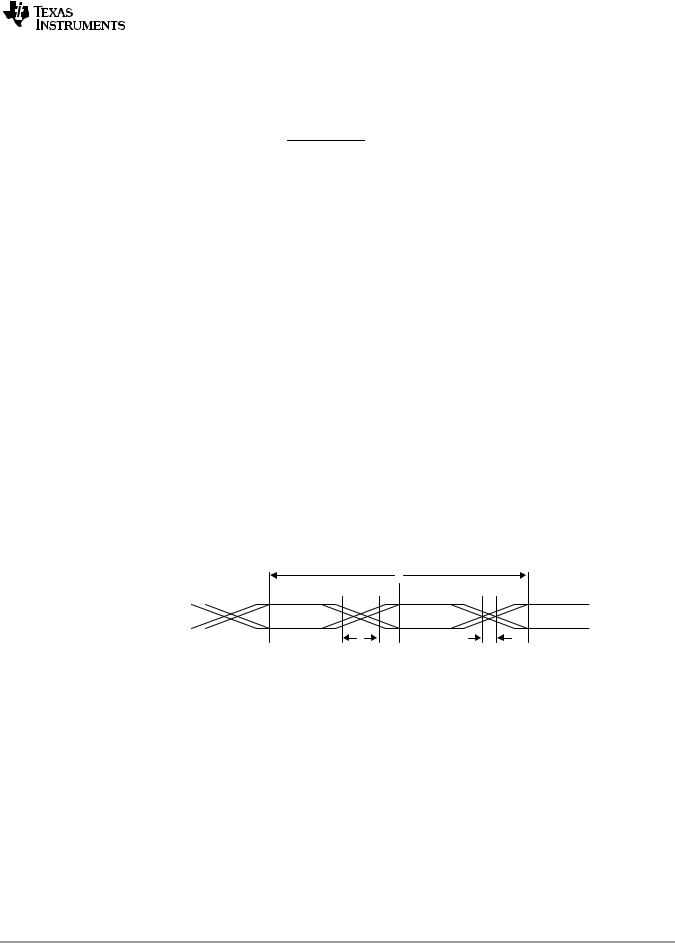
Figure 7-33 DDR3 PLL DDRCLK Timing
1
2
3
DDRCLKN
DDRCLKP
4 |
5 |
7.10 PASS PLL
The PASS PLL generates interface clocks for the Packet Accelerator Subsystem. Using the PACLKSEL pin the user can select the input source of PASS PLL as either the output of Main PLL mux or the PASSCLK clock reference sources. When coming out of power-on reset, PASS PLL comes out in a bypass mode and needs to be programmed to a valid frequency before being enabled and used.
PASS PLL power is supplied externally via the Main PLL power-supply pin (AVDDA3). An external EMI filter circuit must be added to all PLL supplies. Please see the Hardware Design Guide for KeyStone Devices in ‘‘Related Documentation from Texas Instruments’’ on page 59 for detailed recommendations. For the best performance, TI recommends that all the PLL external components be on a single side of the board without jumpers, switches, or components other than those shown. For reduced PLL jitter, maximize the spacing between switching signal traces and the PLL external components (C1, C2, and the EMI Filter).
Copyright 2011 Texas Instruments Incorporated |
169 |
INFORMATION ADVANCE
TMS320TCI6618 |
|
|
|
Communications Infrastructure KeyStone SoC |
|
|
|
SPRS688—February 2011 |
|
www.ti.com |
|
|
|
||
Figure 7-34 PASS PLL Block Diagram |
|
|
|
SYSCLK(P|N) |
REFCLK |
Main PLL and |
|
|
|||
ALTCORECLK(P|N) |
|
PLL Controller |
|
|
|
||
CORECLKSEL |
|
|
|
PASS PLL |
|
/2 |
|
PLLOUT |
Packet |
||
|
|||
PASSCLK(P|N) |
|
Accelerator |
|
xPLLM |
|
|
|
PACLKSEL |
|
|
7.10.1 PASS PLL Control Register
The PASS PLL, which is used to drive the packet accelerator sub-system, does not use a PLL controller. PASS PLL can be controlled using the PAPLLCTL register located in Bootcfg module. This MMR exists inside the Bootcfg space. To write to this register, software should go through an un-locking sequence using KICK0/KICK1 registers. For suggested configurable values see 2.5.3 ‘‘PLL Settings’’ on page 33. See 3.3.4 ‘‘Kicker Mechanism (KICK0 and KICK1) Register’’ on page 65 for the address location of the registers and locking and unlocking sequences for accessing the registers. This register is reset on POR only.
. |
PASS PLL Control Register (PASSPLLCTL) (1) |
|
|
|
|
||||
Figure 7-35 |
|
|
|
|
|||||
31 |
|
24 |
23 |
22 |
19 |
18 |
6 |
5 |
0 |
|
|
|
|
|
|
|
|
||
BWADJ[7:0] |
|
BYPASS |
Reserved |
PLLM |
|
|
PLLD |
||
|
|
|
|
|
|
|
|||
RW,+0000 1001 |
|
RW,+0 |
RW,+0001 |
RW,+0000000010011 |
|
RW,+000000 |
Legend: RW = Read/Write; -n = value after reset
1 This register is Reset on POR only. The regreset, reset, and bgreset from PLL are all tied to a common pll0_ctrl_rst_n. The pwrdn, regpwrdn, and bgpwrdn are all tied to common pll0_ctrl_to_pll_pwrdn.
Table 7-63 |
PASS PLL Control Register Field Descriptions |
||
|
|
|
|
Bit |
Field |
|
Description |
31-24 |
BWADJ[7:0] |
BWADJ should be programmed to a value equal to half of PLLM[12:0]. Example: PLLM = 15, then BWADJ = 7 |
|
|
|
|
|
23 |
BYPASS |
|
Enable Bypass Mode |
|
|
|
0 = Bypass Disabled |
|
|
|
1 = Bypass Enabled |
|
|
|
|
22-19 |
Reserved |
Reserved |
|
|
|
|
|
18-6 |
PLLM |
|
A 13-bit bus that selects the values for the multiplication factor (see Note below) |
|
|
|
|
5-0 |
PLLD |
|
A 6-bit bus that selects the values for the reference divider |
|
|
|
|
End of Table 7-63 |
|
||
|
|
|
|
7.10.2 PASS PLL Device-Specific Information
As shown in Figure 7-34, the output of PASS PLL (PLLOUT) is divided by 2 and directly fed to the Packet Accelerator Sub-System. The PASS PLL is affected by power-on reset. During power-on resets, the internal clocks of the PASS PLL are affected as described in Section 7.7 ‘‘Reset Controller’’ on page 149. PASS PLL is unlocked only during the power-up sequence and is locked by the time the RESETSTAT pin goes high. It does not lose lock during any of the other resets.
170 |
Copyright 2011 Texas Instruments Incorporated |
|
|
|
|
|
|
TMS320TCI6618 |
||
|
|
|
|
Communications Infrastructure KeyStone SoC |
||||
www.ti.com |
|
|
|
|
SPRS688—February 2011 |
|||
|
|
|
|
|
|
|
||
7.10.3 PASS PLL Input Clock Electrical Data/Timing |
|
|
|
|
||||
Table 7-64 |
PASS PLL Timing Requirements |
|
|
|
|
|||
(See Figure 7-36 and Figure 7-30) |
|
|
|
|
||||
|
|
|
|
|
|
|
|
|
No. |
|
|
|
Parameter |
Min |
Max |
Unit |
|
|
|
|
|
PASSCLK[P:N] |
|
|
|
|
|
|
|
|
|
|
|
|
|
1 |
|
tc(PASSCLKN) |
Cycle Time _ PASSCLKN cycle time |
3.2 |
25 |
ns |
|
|
|
|
|
|
|
|
|
|
|
1 |
|
tc(PASSCLKP) |
Cycle Time _ PASSCLKP cycle time |
3.2 |
25 |
ns |
|
|
|
|
|
|
|
|
|
|
|
3 |
|
tw(PASSCLKN) |
Pulse Width _ PASSCLKN high |
0.45*tc(PASSCLKN) |
0.55*tc(PASSCLKN) |
ns |
|
|
|
|
|
|
|
|
|
|
|
2 |
|
tw(PASSCLKN) |
Pulse Width _ PASSCLKN low |
0.45*tc(PASSCLKN) |
0.55*tc(PASSCLKN) |
ns |
|
|
|
|
|
|
|
|
|
|
|
2 |
|
tw(PASSCLKP) |
Pulse Width _ PASSCLKP high |
0.45*tc(PASSCLKP) |
0.55*tc(PASSCLKP) |
ns |
|
|
|
|
|
|
|
|
|
|
|
3 |
|
tw(PASSCLKP) |
Pulse Width _ PASSCLKP low |
0.45*tc(PASSCLKP) |
0.55*tc(PASSCLKP) |
ns |
|
|
|
|
|
|
|
|
|
|
|
4 |
|
tr(PASSCLKN_250mv) |
Transition Time _ PASSCLKN Rise time (250 mV) |
50 |
350 |
ps |
|
|
|
|
|
|
|
|
|
|
|
4 |
|
tf(PASSCLKN_250mv) |
Transition Time _ PASSCLKN Fall time (250 mV) |
50 |
350 |
ps |
|
|
|
|
|
|
|
|
|
|
|
4 |
|
tr(PASSCLKP_250mv) |
Transition Time _ PASSCLKP Rise time (250 mV) |
50 |
350 |
ps |
|
|
|
|
|
|
|
|
|
|
|
4 |
|
tf(PASSCLKP_250mv) |
Transition Time _ PASSCLKP Fall time (250 mV) |
50 |
350 |
ps |
|
|
|
|
|
|
|
|
|
|
|
5 |
|
tj(PASSCLKN) |
Jitter, Peak_to_Peak _ Periodic PASSCLKN |
|
100 |
ps, pk-pk |
|
|
|
|
|
|
|
|
|
|
|
5 |
|
tj(PASSCLKP) |
Jitter, Peak_to_Peak _ Periodic PASSCLKP |
|
100 |
ps, pk-pk |
|
|
|
|
|
|
|
|
|
|
|
Figure 7-36 PASS PLL Timing
1
2
3
PASSCLKN
PASSCLKP
4 |
5 |
ADVANCE INFORMATION
Copyright 2011 Texas Instruments Incorporated |
171 |