

- •Release History
- •Contents
- •List of Figures
- •List of Tables
- •1 TMS320TCI6618 Features
- •1.1 KeyStone Architecture
- •1.2 Device Description
- •1.3 Functional Block Diagram
- •2 Device Overview
- •2.1 Device Characteristics
- •2.2 CPU (DSP Core) Description
- •2.3 Memory Map Summary
- •2.4 Boot Sequence
- •2.5 Boot Modes Supported and PLL Settings
- •2.5.1 Boot Device Field
- •2.5.2 Device Configuration Field
- •2.5.2.1 No Boot Device Configuration
- •2.5.2.2 Serial Rapid I/O Boot Device Configuration
- •2.5.2.3 Ethernet (SGMII) Boot Device Configuration
- •2.5.2.4 PCI Boot Device Configuration
- •2.5.2.5 I2C Boot Device Configuration
- •2.5.2.6 SPI Boot Device Configuration
- •2.5.2.7 HyperLink Boot Device Configuration
- •2.5.3 PLL Settings
- •2.6 Second-Level Bootloaders
- •2.7 Terminals
- •2.8 Terminal Functions
- •2.9 Development
- •2.9.1 Development Support
- •2.9.2 Device Support
- •Related Documentation from Texas Instruments
- •3 Device Configuration
- •3.1 Device Configuration at Device Reset
- •3.2 Peripheral Selection After Device Reset
- •3.3 Device State Control Registers
- •3.3.1 Device Status (DEVSTAT) Register
- •3.3.2 Device Configuration Register
- •3.3.3 JTAG ID (JTAGID) Register Description
- •3.3.4 Kicker Mechanism (KICK0 and KICK1) Register
- •3.3.5 LRESETNMI PIN Status (LRSTNMIPINSTAT) Register
- •3.3.6 LRESETNMI PIN Status Clear (LRSTNMIPINSTAT_CLR) Register
- •3.3.7 Reset Status (RESET_STAT) Register
- •3.3.8 Reset Status Clear (RESET_STAT_CLR) Register
- •3.3.9 Boot Complete (BOOTCOMPLETE) Register
- •3.3.10 Power State Control (PWRSTATECTL) Register
- •3.3.11 NMI Even Generation to CorePac (NMIGRx) Register
- •3.3.12 IPC Generation (IPCGRx) Registers
- •3.3.13 IPC Acknowledgement (IPCARx) Registers
- •3.3.14 IPC Generation Host (IPCGRH) Register
- •3.3.15 IPC Acknowledgement Host (IPCARH) Register
- •3.3.16 Timer Input Selection Register (TINPSEL)
- •3.3.17 Timer Output Selection Register (TOUTPSEL)
- •3.3.18 Reset Mux (RSTMUXx) Register
- •3.4 Pullup/Pulldown Resistors
- •4 System Interconnect
- •4.1 Internal Buses, Bridges, and Switch Fabrics
- •4.2 Data Switch Fabric Connections
- •4.3 Configuration Switch Fabric
- •4.4 Bus Priorities
- •5 C66x CorePac
- •5.1 Memory Architecture
- •5.1.1 L1P Memory
- •5.1.2 L1D Memory
- •5.1.3 L2 Memory
- •5.1.4 MSM SRAM
- •5.1.5 L3 Memory
- •5.2 Memory Protection
- •5.3 Bandwidth Management
- •5.4 Power-Down Control
- •5.5 CorePac Resets
- •5.6 CorePac Revision
- •5.7 C66x CorePac Register Descriptions
- •6 Device Operating Conditions
- •6.1 Absolute Maximum Ratings
- •6.2 Recommended Operating Conditions
- •6.3 Electrical Characteristics
- •7 TMS320TCI6618 Peripheral Information and Electrical Specifications
- •7.1 Parameter Information
- •7.1.1 1.8-V Signal Transition Levels
- •7.1.2 Timing Parameters and Board Routing Analysis
- •7.2 Recommended Clock and Control Signal Transition Behavior
- •7.3 Power Supplies
- •7.3.1 Power-Up Sequencing
- •7.3.1.1 Core-Before-IO Power Sequencing
- •7.3.1.2 IO-Before-Core Power Sequencing
- •7.3.1.3 Prolonged Resets
- •7.3.2 Power-Down Sequence
- •7.3.3 Power Supply Decoupling and Bulk Capacitors
- •7.3.4 SmartReflex
- •7.4 Enhanced Direct Memory Access (EDMA3) Controller
- •7.4.1 EDMA3 Device-Specific Information
- •7.4.2 EDMA3 Channel Synchronization Events
- •7.5 Interrupts
- •7.5.1 Interrupt Sources and Interrupt Controller
- •7.5.2 INTC Registers
- •7.5.2.1 INTC0 Register Map
- •7.5.2.2 INTC1 Register Map
- •7.5.2.3 INTC2 Register Map
- •7.5.3 Inter-Processor Register Map
- •7.5.4 NMI and LRESET
- •7.5.5 External Interrupts Electrical Data/Timing
- •7.6 Memory Protection Unit (MPU)
- •7.6.1 MPU Registers
- •7.6.1.1 MPU Register Map
- •7.6.1.2 Device-Specific MPU Registers
- •7.6.2 MPU Programmable Range Registers
- •7.6.2.1 Programmable Range n Start Address Register (PROGn_MPSAR)
- •7.6.2.2 Programmable Range n - End Address Register (PROGn_MPEAR)
- •7.6.2.3 Programmable Range n Memory Protection Page Attribute Register (PROGn_MPPA)
- •7.7 Reset Controller
- •7.7.1 Power-on Reset
- •7.7.2 Hard Reset
- •7.7.3 Soft Reset
- •7.7.4 Local Reset
- •7.7.5 Reset Priority
- •7.7.6 Reset Controller Register
- •7.7.7 Reset Electrical Data/Timing
- •7.8 Main PLL and the PLL Controller
- •7.8.1 Main PLL Controller Device-Specific Information
- •7.8.1.1 Internal Clocks and Maximum Operating Frequencies
- •7.8.1.2 Main PLL Controller Operating Modes
- •7.8.1.3 Main PLL Stabilization, Lock, and Reset Times
- •7.8.2 PLL Controller Memory Map
- •7.8.2.1 PLL Secondary Control Register (SECCTL)
- •7.8.2.2 PLL Controller Divider Register (PLLDIV2, PLLDIV5, PLLDIV8)
- •7.8.2.3 PLL Controller Clock Align Control Register (ALNCTL)
- •7.8.2.4 PLLDIV Divider Ratio Change Status Register (DCHANGE)
- •7.8.2.5 SYSCLK Status Register (SYSTAT)
- •7.8.2.6 Reset Type Status Register (RSTYPE)
- •7.8.2.7 Reset Control Register (RSTCTRL)
- •7.8.2.8 Reset Configuration Register (RSTCFG)
- •7.8.2.9 Reset Isolation Register (RSISO)
- •7.8.3 Main PLL Control Registers
- •7.8.4 Main PLL Controller/SRIO/HyperLink/PCIe Clock Input Electrical Data/Timing
- •7.9.1 DDR3 PLL Control Register
- •7.9.2 DDR3 PLL Device-Specific Information
- •7.9.3 DDR3 PLL Input Clock Electrical Data/Timing
- •7.10 PASS PLL
- •7.10.1 PASS PLL Control Register
- •7.10.2 PASS PLL Device-Specific Information
- •7.10.3 PASS PLL Input Clock Electrical Data/Timing
- •7.11 DDR3 Memory Controller
- •7.11.1 DDR3 Memory Controller Device-Specific Information
- •7.11.2 DDR3 Memory Controller Electrical Data/Timing
- •7.12 I2C Peripheral
- •7.12.1 I2C Device-Specific Information
- •7.12.2 I2C Peripheral Register Description(s)
- •7.12.3 I2C Electrical Data/Timing
- •7.12.3.1 Inter-Integrated Circuits (I2C) Timing
- •7.13 SPI Peripheral
- •7.13.1 SPI Electrical Data/Timing
- •7.13.1.1 SPI Timing
- •7.14 HyperLink Peripheral
- •7.15 UART Peripheral
- •7.16 PCIe Peripheral
- •7.17 Packet Accelerator
- •7.18 Security Accelerator
- •7.19 Ethernet MAC (EMAC)
- •7.20 Management Data Input/Output (MDIO)
- •7.21 Timers
- •7.21.1 Timers Device-Specific Information
- •7.21.2 Timers Electrical Data/Timing
- •7.22 Rake Search Accelerator (RSA)
- •7.23 Enhanced Viterbi-Decoder Coprocessor (VCP2)
- •7.24 Third-Generation Turbo Decoder Coprocessor (TCP3d)
- •7.25 Turbo Encoder Coprocessor (TCP3e)
- •7.26 Bit Rate Coprocessor (BCP)
- •7.27 Serial RapidIO (SRIO) Port
- •7.28 General-Purpose Input/Output (GPIO)
- •7.28.1 GPIO Device-Specific Information
- •7.28.2 GPIO Electrical Data/Timing
- •7.29 Semaphore2
- •7.30 Antenna Interface Subsystem 2
- •7.33 FFTC
- •7.34 Emulation Features and Capability
- •7.34.1 Advanced Event Triggering (AET)
- •7.34.2 Trace
- •7.34.2.1 Trace Electrical Data/Timing
- •7.34.3 IEEE 1149.1 JTAG
- •7.34.3.1 IEEE 1149.1 JTAG Compatibility Statement
- •7.34.3.2 JTAG Electrical Data/Timing
- •8 Mechanical Data
- •8.1 Packaging Information
- •8.2 Package CYP
|
|
|
|
|
|
|
|
|
|
|
|
|
|
|
|
|
|
|
|
|
|
|
|
|
|
|
|
TMS320TCI6618 |
|||
|
|
|
|
|
|
|
|
|
|
|
|
|
|
|
|
|
|
|
|
|
|
Communications Infrastructure KeyStone SoC |
|||||||||
www.ti.com |
|
|
|
|
|
|
|
|
|
|
|
|
|
|
|
|
|
|
|
|
|
SPRS688—February 2011 |
|||||||||
|
|
|
|
|
|
|
|
|
|
|
|
|
|
|
|
|
|
|
|
|
|
|
|
|
|
||||||
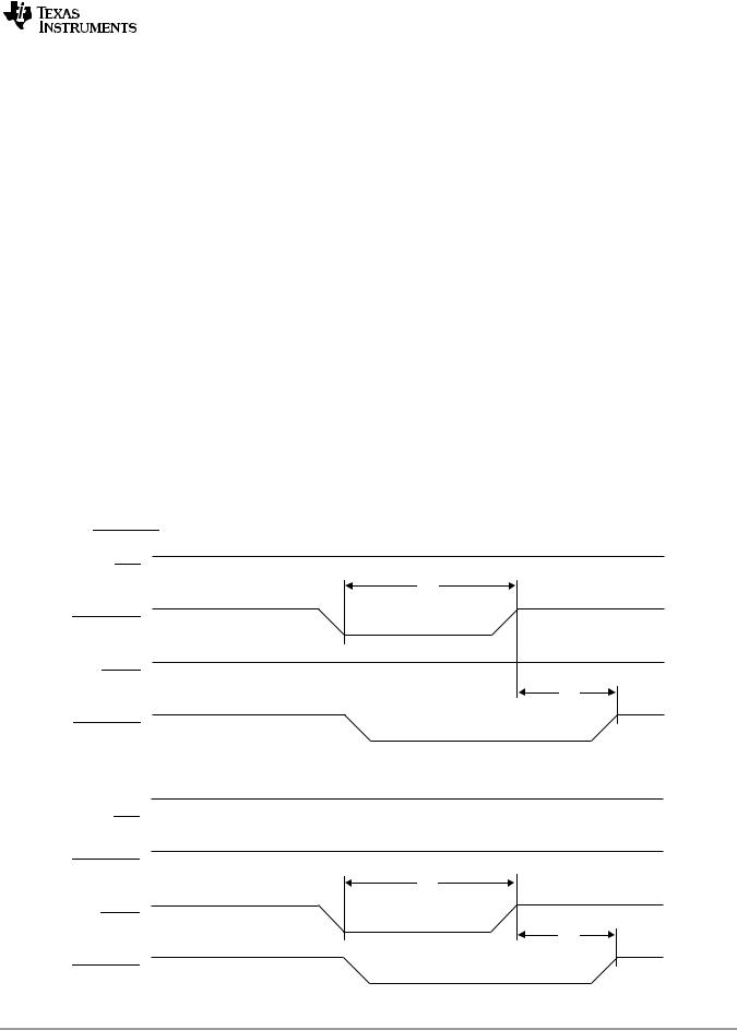
7.7.7 Reset Electrical Data/Timing |
|
|
|
|
|
||||||||||||||||||||||||||
Table 7-44 |
Reset Timing Requirements (1) (2) |
|
|
|
|
|
|||||||||||||||||||||||||
(see Figure 7-14 and Figure 7-15) |
|
|
|
|
|
|
|
|
|
|
|
|
|
|
|
|
|
|
|
|
|||||||||||
|
|
|
|
|
|
|
|
|
|
|
|
|
|
|
|
|
|
|
|
|
|
|
|
|
|
|
|
|
|
|
|
No. |
|
|
|
|
|
|
|
|
|
|
|
|
|
|
|
|
|
|
|
|
|
|
|
|
|
|
Min |
Max |
Unit |
|
|
|
|
|
|
|
|
|
|
|
|
|
|
|
|
|
|
|
|
|
|
|
|
Pin Reset |
|
|
|
|
|
||||
|
|
|
|
|
|
|
|
|
|
|
|
|
|
|
|
|
RESETFULL |
|
|
|
|
|
|||||||||
1 |
|
|
|
|
|
|
|
|
|
|
|
Pulse Width - Pulse width |
|
|
|
|
low |
500C |
|
|
ns |
|
|||||||||
tw(RESETFULL) |
RESETFULL |
|
|
||||||||||||||||||||||||||||
|
|
|
|
|
|
|
|
|
|
|
|
|
|
|
|
|
Soft/Hard-Reset |
|
|
|
|
|
|||||||||
|
|
|
|
|
|
|
|
|
|
|
|
|
|
|
|
|
|
|
|
|
|
|
|
|
|
|
|||||
3 |
|
tw(RESET) |
|
|
|
|
|
|
|
Pulse Width - Pulse width RESET low |
500C |
|
|
ns |
|
||||||||||||||||
End of Table 7-44 |
|
|
|
|
|
|
|
|
|
|
|
|
|
|
|
|
|
|
|
|
|||||||||||
|
|
|
|
|
|
|
|
|
|
||||||||||||||||||||||
1 If CORECLKSEL = 0, C = 1 ÷ CORECLK(N|P) frequency in ns. |
|
|
|
|
|
||||||||||||||||||||||||||
2 If CORECLKSEL = 1, C = 1 ÷ ALTCORECLK frequency in ns. |
|
|
|
|
|
||||||||||||||||||||||||||
Table 7-45 |
Reset Switching Characteristics Over Recommended Operating Conditions (1) (2) |
|
|
|
|
|
|||||||||||||||||||||||||
(see Figure 7-14 and Figure 7-15) |
|
|
|
|
|
|
|
|
|
|
|
|
|
|
|
|
|
|
|
|
|||||||||||
|
|
|
|
|
|
|
|
|
|
|
|
|
|
|
|
|
|
|
|
|
|
|
|
|
|
|
|
||||
No. |
|
|
|
|
|
|
|
|
|
|
|
|
Parameter |
|
Min |
Max |
|
Unit |
|
||||||||||||
|
|
|
|
|
|
|
|
|
|
|
|
|
|
|
|
|
|
|
|
|
Pin Reset |
|
|
|
|
|
|||||
|
|
|
|
|
|
|
|
|
|
|
|
|
|
|
|
|
RESETFULL |
|
|
|
|
|
|||||||||
2 |
|
|
|
|
|
|
|
- |
|
|
|
|
Delay Time - |
|
|
|
high after |
|
|
high |
|
|
50000C |
|
ns |
|
|||||
td(RESETFULLH |
RESETSTATH) |
RESETSTAT |
RESETFULL |
|
|||||||||||||||||||||||||||
|
|
|
|
|
|
|
|
|
|
|
|
|
|
|
|
|
Soft/Hard Reset |
|
|
|
|
|
|||||||||
4 |
|
td(RESETH |
- |
RESETSTATH) |
|
|
|
Delay Time - |
RESETSTAT |
high after |
RESET |
high |
|
|
50000C |
|
ns |
|
|||||||||||||
End of Table 7-45 |
|
|
|
|
|
|
|
|
|
|
|
|
|
|
|
|
|
|
|
|
|||||||||||
|
|
|
|
|
|
|
|
|
|
|
|
|
|
|
|
|
|
|
|
|
|
|
|
|
|
|
|
|
|
|
|
1 If CORECLKSEL = 0, C = 1 ÷ CORECLK(N|P) frequency in ns. 2 If CORECLKSEL = 1, C = 1 ÷ ALTCORECLK frequency in ns.
Figure 7-14 RESETFULL Reset Timing
POR
1
RESETFULL
RESET
3
RESETSTAT
Figure 7-15 Soft/Hard Reset Timing
POR
RESETFULL
2
RESET
4
RESETSTAT
ADVANCE INFORMATION
Copyright 2011 Texas Instruments Incorporated |
153 |
INFORMATION ADVANCE
TMS320TCI6618 |
|
|
|
|
|
|
|
|
||||||
Communications Infrastructure KeyStone SoC |
|
|
|
|||||||||||
SPRS688—February 2011 |
|
|
|
|
|
|
|
www.ti.com |
||||||
|
|
|
|
|
|
|
|
|
|
|
|
|
|
|
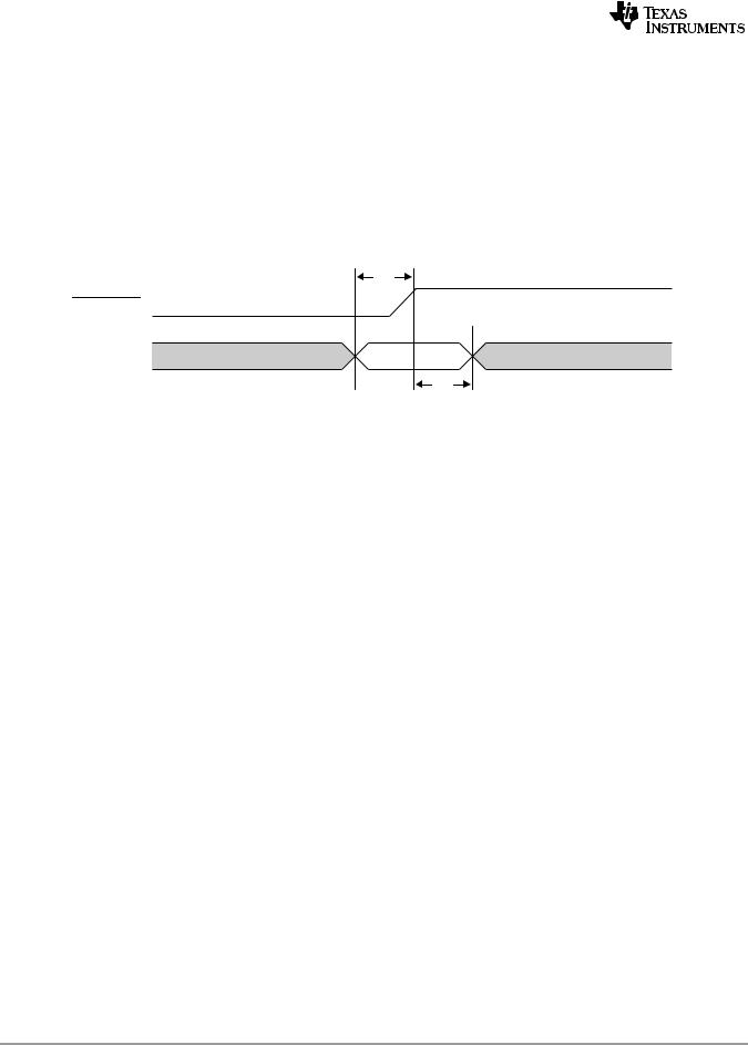
Table 7-46 |
Boot Configuration Timing Requirements (1) (2) |
|
|
|
||||||||||
See Figure 7-16) |
|
|
|
|
|
|
|
|
|
|
|
|
||
|
|
|
|
|
|
|
|
|
|
|
|
|
|
|
No. |
|
|
|
|
|
|
|
|
|
|
|
Min |
Max |
Unit |
1 |
tsu(GPIOn- |
|
|
|
Setup Time - GPIO valid before |
|
|
asserted |
12C |
|
ns |
|||
RESETFULL) |
RESETFULL |
|
||||||||||||
2 |
|
|
|
|
-GPIOn) |
Hold Time - GPIO valid after |
|
|
asserted |
12C |
|
ns |
||
th(RESETFULL |
RESETFULL |
|
||||||||||||
End of Table 7-46 |
|
|
|
|
|
|
|
|
||||||
|
|
|
|
|
|
|
|
|
|
|
|
|
|
|
1 If CORECLKSEL = 0, C = 1 ÷ CORECLK(N|P) frequency in ns. 2 If CORECLKSEL = 1, C = 1 ÷ ALTCORECLK frequency in ns.
Figure 7-16 Boot Configuration Timing
1
RESETFULL
GPIO[15:0]
2
154 |
Copyright 2011 Texas Instruments Incorporated |