

3.3pv Cell Technologies
In making comparisons between alternative power technologies, the most important measure is the energy cost per kWh delivered. In pv power, this cost primarily depends on two parameters, the photovoltaic energy conversion efficiency, and the capital cost per watt capacity. Together, these two parameters indicate the economic competitiveness of the pv electricity.
The conversion efficiency of the photovoltaic cell is defined as follows:
η = |
electrical power output |
|
solar power impinging the cell
The continuing development efforts to produce more efficient low cost cells have resulted in various types of pv technologies available in the market today, in terms of the conversion efficiency and the module cost. The major types are discussed in the following sections:1
3.3.1Single-Crystalline Silicon
The single crystal silicon is the widely available cell material, and has been the workhorse of the industry. In the most common method of producing this material, the silicon raw material is first melted and purified in a crucible. A seed crystal is then placed in the liquid silicon and drawn at a slow constant rate. This results in a solid, single-crystal cylindrical ingot (Figure 3-12). The manufacturing process is slow and energy intensive, resulting in high raw material cost presently at $25 to $30 per pound. The ingot is sliced using a diamond saw into 200 to 400 µm (0.005 to 0.010 inch) thick wafers. The wafers are further cut into rectangular cells to maximize the number of cells that can be mounted together on a rectangular panel. Unfortunately, almost half of the expensive silicon ingot is wasted in slicing ingot and forming square cells. The material waste can be minimized by making the full size round cells from round ingots (Figure 3-13). Using such cells would be economical where the panel space is not at a premium. Another way to minimize the waste is to grow crystals on ribbons. Some U.S. companies have set up plants to draw pv ribbons, which are then cut by laser to reduce waste.
3.3.2Polycrystalline and Semicrystalline
This is relatively a fast and low cost process to manufacture thick crystalline cells. Instead of drawing single crystals using seeds, the molten silicon is cast into ingots. In the process, it forms multiple crystals. The conversion efficiency is lower, but the cost is much lower, giving a net reduction in cost per watt of power.
© 1999 by CRC Press LLC
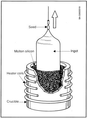
FIGURE 3-12
Single-crystal ingot-making by Czochralski process. (Source: Cook, G., Photovoltaic Fundamental, DOE/NREL Report DE91015001, February 1995.)
3.3.3Thin Films
These are new types of photovoltaics entering the market. Copper Indium Diselenide, Cadmium Telluride, and Gallium Arsenide are all thin film materials, typically a few µm or less in thickness, directly deposited on glass, stainless steel, ceramic or other compatible substrate materials. This technology uses much less material per square area of the cell, hence, is less expensive per watt of power generated.
3.3.4Amorphous Silicon
In this technology, amorphous silicon vapor is deposited on a couple of µmthick amorphous (glassy) films on stainless steel rolls, typically 2,000-feet long and 13-inches wide. Compared to the crystalline silicon, this technology uses only 1 percent of the material. Its efficiency is about one-half of the crystalline silicon at present, but the cost per watt generated is projected to
© 1999 by CRC Press LLC
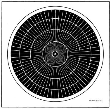
FIGURE 3-13
Round-shape pv cell reduces material waste typically found in rectangular cell. (Depiction based on cell used by Applied Solar Energy Corporation, City of Industry, California.)
be significantly lower. On this premise, two large plants to manufacture amorphous silicon panels started in the U.S.A. in 1996.
3.3.5Spheral
This is yet another technology that is being explored in the laboratories. The raw material is low-grade silicon crystalline beads, presently costing about $1 per pound. The beads are applied on typically 4-inch squares of thin perforated aluminum foil. In the process, the impurities are pushed to the surface, from where they are etched away. Since each sphere works independently, the individual sphere failure has negligible impact on the average performance of the bulk surface. According to a Southern California Edison Company’s estimate, 100 square feet of spheral panels can generate 2,000 kWh per year in an average southern California climate.
© 1999 by CRC Press LLC
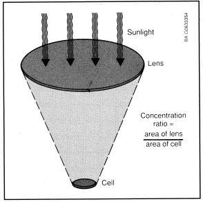
FIGURE 3-14
Lens concentrating the sunlight on small area reduces the need of active cell material. (Source: Photovoltaic Fundamental, DOE/NREL Report DE91015001, February 1995.)
3.3.6Concentrated Cells
In an attempt to improve the conversion efficiency, the sunlight is concentrated into tens or hundreds of times the normal sun intensity by focusing on a small area using low cost lenses (Figure 3-14). The primary advantage is that such cells require a small fraction of area compared to the standard cells, thus significantly reducing the pv material requirement. However, the total module area remains the same to collect the required sun power. Besides increasing the power and reducing the size or number of cells, such cells have additional advantage that the cell efficiency increases under concentrated light up to a point. Another advantage is that they can use small area cells. It is easier to produce high efficiency cells of small areas than to produce large area cells with comparable efficiency. On the other hand, the major disadvantage of the concentrator cells is that they require focusing optics adding into the cost.
The annual production of various pv cells in 1995 is shown in Table 3-1. Almost all production has been in the crystalline silicon and the amorphous silicon cells, with other types being in the development stage. The present status of the crystalline silicon and the amorphous silicon technologies is shown in Table 3-2. The former is dominant in the market at present and the latter is expected to be dominant in the near future.
© 1999 by CRC Press LLC