

Parker K.P.Effects of defects on high-speed boards
.pdfThe Effects of Defects on High-Speed Boards
Kenneth P. Parker
Agilent Technologies
Loveland, CO
kenneth_parker at agilent dot com
Abstract
Printed circuit boards are steadily becoming faster. They have higher clock speeds, and edge rates on data signals have dropped down into the 100’s of picoseconds. This presents some new challenges to the board test world because certain defects we did not do a good job covering in the past can no longer be ignored.
1 Introduction
With the advances made in ICs due to Moore’s Law, we can achieve spectacular data rates on-chip. Data rates at the board level are almost always slower such that they become an architectural limiter to overall system speed. Moore’s law allows us to pack more of a system into an IC, and it also allows us to package capabilities (IP) that can be used to change the architecture of a system such that we can achieve new heights of performance. For example, Serialize/Deserialize technology (SerDes) was once used in high-end systems to form high-speed serial links between subsystems. Now we can pack multiple SerDes channels (both transmit and receive) into a single IC and use them to transmit serialized data with embedded clocking between ICs on a single board. This new architecture is replacing parallel buses that needed separate clock distribution systems with complex skew control. SerDes technology is now becoming prevalent in low-end consumer products. PCI-Express [PCIE04] in the personal computer world is a prime example of this trend. The first wave of this standard will start with serial data rates of 2.5 Gigabits/second, and move up to 5, maybe someday even 10 Gbps.
2 High-Speed Signal Propagation (HSSP)
Designing high-speed digital systems [JoGr93] offers design challenges to digital designers. Principally, digital designers find the friendly and clean “digital” world has become full of nasty “analog” surprises. The area most affected is in the attempt to propagate signals across a board or between boards without resorting to exotic transmission techniques such as optical links. As we move from sub-Gigabit boards (still challenging) into the Gigabit range, new care must be taken to design boards that can propagate such signals. Current thinking says that with care, we could eventually achieve 10 Gbps rates on boards using standard processes and materials in
wide use today. Beyond this range, unusual (read, expensive) materials and processes will be needed.
However, a key phrase in the last paragraph was “with care”. Board designers will need to study HSSP design (see [JoGr03]) in order to know what new design techniques will be needed. Suddenly, boards must have well-controlled characteristic impedances which imply strict layout rules. Even such mundane concepts as the design of a via have new engineering considerations. Multiple power and ground pins on ICs (already common today) will continue to be important, and not simply for the mitigation of ground-bounce. Certain “mundane” devices such as bypass capacitors must now be chosen with care, and their placement becomes a critical design problem. Simple connectors are no longer “simple”. They become something more like a waveguide as frequency and data rate rise. Through-hole attachments common for connectors will be forced to change to ball-grid attachments.
2.1Signals and Signal Return Currents
Most “digital people” think more in logic diagram form rather than schematically. This means they think of signals as voltages, when in reality, all signals are carried by currents (albeit small ones). All currents must travel in loops from source, to a load and then back, as in Figure 1. Essentially, the signal wave front can be thought of as charging a series of tiny capacitors between the signal trace and ground, moving from left to right, charging each in succession. Further, the loop encloses an area. Basic physics tells us that current flowing in a loop creates a magnetic field. This field is stronger for larger loop areas and weaker for smaller areas. The combination of capacitance and inductance creates a transmission line.
Signal Propagation
Termination
Signal Return Current
Figure 1: A signal is carried by current that flows in a loop. Current must return to the driver by the signal return path.
Copyright © Agilent Technologies 2004. To appear at the 2004 IEEE Board Test Workshop.
Transmission lines are fundamental to HSSP. Designers strive to create a uniform structure for a transmission line. For a given structure, there will be a certain capacitance and inductance per unit length. If either of these variables change at some point due to some non-uniformity, the transmission line impedance changes too. This discontinuity in the impedance will cause waveform degradation by reflecting some energy in the reverse direction it came from. Multiple reflections may occur, causing a waveform to interact with reducedamplitude copies of its previous shape. A neat pulse can end up looking like a series of positive and negative wiggles, unrecognizable from the original. To further complicate matters, the choice of a signal return path is frequency-dependent.
2.2Low and High Frequency Signal Return Paths
DC and low frequencies return to the driver by a pathway in the ground plane that minimizes resistance. Current spreads out over the plane to minimize the amount of resistance in the path as shown in Figure 2.
Ground Plane
Figure 2: DC signal return current spreads out across the ground plane to minimize resistance.
However, for higher frequencies, the path taken by current is determined by inductance. The path that has the minimum amount of inductance will carry the majority of the current as shown in Figure 3.
Ground Plane
Figure 3: High frequency return current will follow the path of least inductance, directly under the signal.
The path of least inductance will be that which minimizes the total area of the loop the current travels in. This path is directly below the signal trace on the ground plane. So, even though there is lots of copper area for the signal to travel through, it will confine itself to a small region as close to the signal trace as it can get. Sometimes this is called “mirror current”.
If there is some discontinuity in the ground plane that forces the current to take a longer path, this has the effect of increasing the area of the loop, which increases
its inductance. This will have the effect of changing the impedance of the path at that point, causing waveform degradation. It also increases the amount of high frequency radiation the loop generates. This can increase interference (RFI) generated by the overall design.
3 The Impact of HSSP on Test Coverage
What does all this mean to test engineers? After all, they test boards today with low-speed technologies such as In-Circuit test (ICT), and/or use inspection technologies such as Automatic Optical Inspection (AOI) or Automatic X-Ray Inspection (AXI) that don’t use electrical methods at all. Why is HSSP of concern for test?
The answer to this comes from a study of what defects your current test strategy can find, and those it has trouble finding. Focus for a moment on In-Circuit test. The PCOLA/SOQ defect model proposed by Hird et al [Hird02] gives us a defect model very useful for illustrating the problem presented by HSSP. When a skilled test engineer develops an excellent ICT test for a board, a coverage measurement for that test will still have notable blind spots. There are three of concern for HSSP boards:
1.Opens on ground pins in connectors and sockets
2.Missing or open bypass capacitors
3.Opens on power/ground pins on ICs
All of these defects are essentially untestable by normal ICT methods. One can augment ICT coverage with AOI or AXI. AOI should do well finding missing bypass caps, but will be challenged by the prevalence of BGA attachments that HSSP will demand. AXI will be able to “see” such joints, but is often not practical to use AXI on lower-end products due to throughput limitations and system cost. Thus, an ICT-only strategy may be the best coverage we can get. Past experience has said to us that these blind spots did not matter because there was plenty of “redundancy” and a missing bypass or open ground pin could be tolerated. Now the question is, how will HSSP blind spots affect board test?
Because of space limitations, the rest of this paper will concentrate on connector/socket open ground pins. However, the analysis presented will have relevance to the other areas as well.
4 Opens on Connector/Socket Ground Pins
Before HSSP, a connector might have a few power and ground pins used to conduct amperage across a boundary. Many signal pins also existed to carry data. Now, looking at a modern HSSP connector such as PCI Express, one is struck by the fact that nearly ½ of all the pins (29 of 64) are devoted to supplying power or grounding (see Figure 4). Further examination shows that indeed there are some power and ground pins that conduct
Copyright © Agilent Technologies 2004. To appear at the 2004 IEEE Board Test Workshop.

amperage, but most grounds (18 of the 29) are serving as signal return paths.
PCI Express x4 Connector Top View
Power |
Ground |
Signal |
Differential Pair |
Figure 4: PCI Express pin assignments.
A signal return path is of little concern at low frequencies; it merely must exist somewhere. For example, it might be the same ground path that carries amperage. But in HSSP connectors, signal return paths are a critical component of the connector design. This is because the signal return paths are designed to maintain constant impedance through the connector and minimize return path discontinuities. Figure 5 shows a side view of a mother-daughter board connector and the signal path therein. There are some path discontinuities at the driver, receiver and some in the connector. A designer must budget some amount of signal degradation for each such that the overall degradation is within design limits.
Receiver/ Term 


Connector
Drive
r
Signal Plane
FR4
Ground Plane
Figure 5: A mother board, connector and daughter board structure.
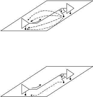
Look again at the connector, this time idealized from the top with two data channels in parallel, as in Figure 6.
The two data channels have their own return paths. Each generates a known amount of magnetic field and there may be some coupling via mutual inductance between them. This is accounted for in the design.
However, if one ground return path is open, then the signal return current for that channel must take a detour to get back to the driver. As before, the current will take the path of lowest inductance, so it will flow directly under the signal trace where it can. When it gets to the connector, it will be forced to take a longer path, as shown in Figure 7. Now the return current for the second driver follows an enlarged path, increasing its inductance and creating an impedance discontinuity. Further, the path shares the connector ground pin of the first driver. Finally, the mutual inductance of the two paths is increased. This allows the two channels to interact more with each other, in the form of crosstalk.
Figure 6: Two data channels through a connector. Each has an independent signal return path.
Open |
joint |
Figure 7: Two data channels with a defect in one return path.
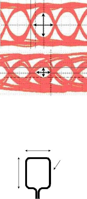
There are two main effects of this defect. The second channel has degraded edge rise/fall times that have the effect of “closing the eye” in an eye diagram in terms of signal swing (see Figure 8). The crosstalk produces jitter in the transition time. This closes the eye in the horizontal (time) dimension. (Both channels are affected.)
As a result of the added signal degradation that now appears in the connector, the signal degradation budget for this design may be exceeded. However, this may not cause an immediately identifiable test failure. For example, say the connector mates with a cable that can be one of several lengths. The board may still be able to drive a 2 or 4 meter cable reliably, but a 10 meter cable may no longer work due to the open ground connection. To find this defect, some sort of functional test will be needed. One could implement a Bit Error Rate Test (BERT) for this channel, but these typically are time - consuming, potentially taking hours. Thus, we have a simple defect (the open pin) with a difficult-to-test failure mode (increased bit error rate).
The added inductance due to the increased loop area can also contribute to electromagnetic radiation that can create interference in other parts of the system. The effects of this interference could be random and infrequent. It could also cause the system to fail
Copyright © Agilent Technologies 2004. To appear at the 2004 IEEE Board Test Workshop.
regulatory requirements for interference transmitted outside the system.
Adequate Eye Opening
Inadequate Eye Opening
Figure 8: Potential eye diagrams for good and faulty connectors.
4.1Theoretical Analysis
We can calculate an approximate change in inductance in a connector signal return path by using a simple model of the loop currents. Start with the equation [JoGr93] in Figure 9 for calculating the inductance of a rectangular loop of wire.
X
Wire
Diameter D
Y
(dimensions in inches)
Loop inductance = 10.16e-9 * [X* ln(2*Y/D) + Y*ln(2*X/D)]
Figure 9: Method of calculating the inductance of a single wire loop.
Next, calculate the defect-free inductance inside the connector. This is done by imagining the channel path shown in Figure 5 where the distance from the driver to the connector, and the distance from the connector to the
receiver are both nearly zero and contribute negligible inductance. Then the loop is defined by the dimensions of the connector itself.
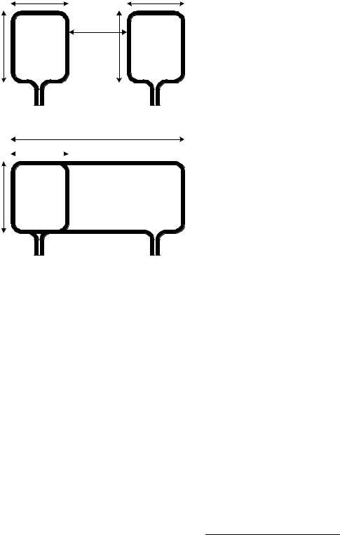
First, set D = 0.015 inch as the diameter of the pin inside the connector. (While this pin is not circular, ignore this distinction in this approximation.) Let Y be the height of the connector. For PCI Express, this is 0.443 inches. The space between pins in a row is X=0.039 inches, where we assume a signal and its ground are adjacent. The formula gives an inductance of this loop of 9.04 nanohenrys.
In the defective case, the value of Y is unchanged. However, the return current now must travel to the next ground pin over. Here, assume the configuration shown in Figure 7. Then the current will travel through the fourth pin so that X is 3 times larger, or 0.117 inches. Now the inductance figures to be 17.2 nanohenrys, for an increase of 8.16 nanohenrys. This seems small, but adding this lumped inductance into the channel adds 51 ohms series impedance at 1 GHz. As frequencies increase, the impe - dance seen will increase. This will degrade edge rates.
Now consider what this increased inductance does to the characteristic impedance of the connector. Assume a 50-ohm system with a transmission line inductance of 7.36 nH/in and capacitance of 2.96 pf/in. Assume the capacitance per inch inside the connector does not change due to the defect so that there is 1.31 pF in 0.443 inches. The inductance over the 0.443 inches is 3.26 nH. The defect then causes the inductance to increase to 11.42 nH. Then the impedance through the length of the connector is:
Z0 = (L/C) 1/2 = (11.42n/1.31p)1/2 = 93 ohms
which is a significant discontinuity. While the distance over which this discontinuity exists is small, faster edges will be affected. Edges that are slower than about 10 times the length of this discontinuity (10*0.443 = 4.4 inches) will not see too much effect. Stated in frequency, signal components less than the speed of light in inches per second divided by this length (1.18028527×10¹⁰/4.4) = 2.7 GHz will be mostly unaffected, while higher frequencies will begin to reflect.
The change in mutual inductance between the faultfree and defective circuits can also be modeled. The defect-free case for the two channels in Figure 6 is shown in Figure 10. The defective case (Figure 7) is shown in Figure 11.
The defect free model shows two independent loops that are separated by a significant space. There will be some coupling between them that will be proportional to the product of the two loop areas and inversely proportional to the cube of the separation. The exact amount of coupling is also dependent on the orientation of the loops to each other, which is a strong function of the connector’s mechanical design.
Copyright © Agilent Technologies 2004. To appear at the 2004 IEEE Board Test Workshop.
|
0.039 |
|
0.039 |
|
|
0.039 |
|
0.443 |
Area A1 = |
0.443 |
Area A2 = |
|
0.017 sq in |
|
0.017 sq in |
Figure 10: Mutual inductance between channels of a defect-free connector.
0.039 |
0.117 |
|
|
0.443 |
Area A1 = |
Area A2 = 0.051 sq in |
0.017 sq in |
Figure 11: Mutual inductance model for an open ground pin.
When the defect is introduced, the defective loop is much larger and overlaps with the defect-free loop. Further, one leg of the loop is shared between them. Exactly how this behaves is complex, so a physical experiment was conducted to see the change in crosstalk that occurs.
4.2Experimental Results
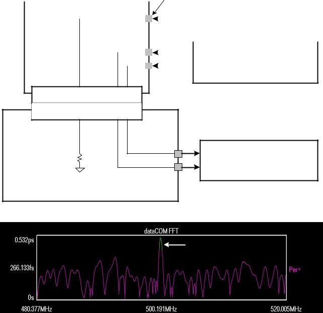
A physical experiment was conducted to see if an open ground pin in a connector could influence data passing through it. The experimental setup is shown in Figure 12.
A PCI Express compliance board set from Intel was used to simulate a data transfer. A PCI Express idle pattern (40 bits) was generated by a pattern generator and supplied in differential form to the add-in card. This data then ran through a PCI Express mated pair of connectors (pins B23 and B24) into the system card where it could be monitored by a Signal Integrity Analyzer. The ground pins around this pair were grounded as required by the PCI Express specification.
A single-ended aggressor signal was generated by a sine-wave signal source and was transmitted onto the addin board and also sent through the connector set on pin B20. It was terminated to ground on the system card. There are two ground pins (B21 and B22) between the aggressor signal and the differential data pair. The aggressor signal was a 1 volt peak-to-peak sine wave set
at 500 MHz. This waveform was chosen because it would show up as a single frequency in a Fast Fourier Transform (FFT) of the received signal.
An open pin defect was simulated by placing electrical tape over ground pin B21.1 Measurements were made with and without the open pin defect present. This “open” is actually fairly capacitive and was probably not a worst-case defect, but we were constrained by concern over damaging the board set which was borrowed.
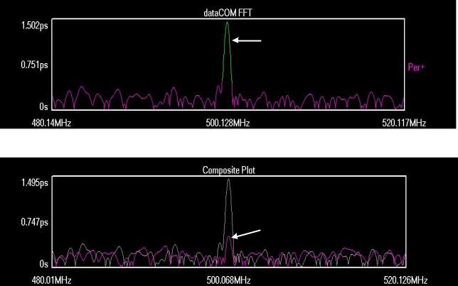
With no defect present, the jitter spectrum in the 500 MHz area appears in Figure 13. There is a small peak at 500 MHz which is the aggressor frequency. Figure 14 shows the same spectrum when the ground pin B21 is opened (with tape). There is a much larger peak at the 500 MHz frequency, showing almost three times the jitter. A composite view of both spectra, centered at 500 MHz appears in Figure 15. This shows that even though there are two ground pins between the aggressor and data paths, one open ground pin will cause an increase in crosstalk between them.
5 Conclusion
With the spread of high-speed designs into common products, we will enter a new era where untested defects of the past are increasingly important. We will need to implement tests for these, or suffer from increased need to do complex functional and system tests. Even then, defective products will be delivered to customers, as some of these defect effects are subtle.
6 Acknowledgements
The author would like to acknowledge valuable conversations about High-Speed Signal Propagation with Dr. Howard Johnson of Signal Consulting Inc. Brad Hegge of Wavecrest Corp performed the signal integrity experiments.
7 |
References |
|
[Hird02] |
“Test Coverage: What Does It Mean when a Board |
|
|
|
Test Passes”, K. Hird, K. P. Parker and B. Follis, |
|
|
Proceedings, International Test Conference, pp |
|
|
1066-1074, Baltimore MD, Oct 2002 |
[JoGr93] |
“High-Speed Digital Design – a Handbook of Black |
|
|
|
Magic”, H. W. Johnson and M. Graham, Prentice |
|
|
Hall PTR, Englewood Cliffs, NJ, 1993 |
[JoGr03] |
“High-Speed Signal Propagation – Advanced Black |
|
|
|
Magic”, H. W. Johnson and M. Graham, Prentice |
|
|
Hall PTR, Englewood Cliffs, NJ, 2003 |
[PCIE04] |
Search the web for “PCI Special Interest Group” or |
|
|
|
PCI-SIG. To get full details, you must be a member |
|
|
of PCI-SIG. |
1 Pin B22 was also opened instead of B21 with no significant change in the observed results. In both cases signal return for data and aggressor current must share a signal return path as seen in Figure 11.
Copyright © Agilent Technologies 2004. To appear at the 2004 IEEE Board Test Workshop.
|
|
|
|
|
|
|
SMA |
|
|
|
|
|
|
|
Connector |
|
|
|
|
|
|
|
|
|
||
Intel PCI Express Compliance |
|
|
|
Agilent 8656B Signal Generator |
||||
Add-In Card |
|
|
|
|
|
|||
|
|
|
|
|||||
|
|
|
|
|
|
|
|
500 MHz sine, 1 volt peak to peak |
|
|
|
|
|
|
|
|
|
|
|
|
|
|
|
|
|
|
|
|
|
|
|
|
|
|
|
|
|
|
|
|
|
|
|
Agilent 70843B Pattern Generator |
|
|
|
|
|
|
|
|
|
|
|
|
|
|
|
|
|
|
B21, B22 |
|
differential |
||||||
|
PCI Express idle pattern |
|||||||
Grounded |
|
|
|
|
|
|||
|
|
|
|
|
3eaa2aaaaa (40 bit) 2.5 Gb/s |
|||
|
|
|
|
|
|
|
|
|
B20 B23 B24
PCI Express Connector Male
PCI Express Connector Female |
||
B20 |
B23 |
B24 |
B21, B22 |
|
|
Grounded |
|
WaveCrest SIA 3000 |
|
term |
|
|
Signal Integrity Analyser |
|
|
|
DataCom FFT mode |
Intel PCI Express Compliance System Board |
||
Figure 12: Experimental setup.
500 MHz
Figure 13: FFT of jitter versus frequency, no defect present, centered at 500 MHz.
Copyright © Agilent Technologies 2004. To appear at the 2004 IEEE Board Test Workshop.
500 MHz
Figure 14: FFT when pin B21 is open, centered at 500 MHz.
 500 MHz aggressor, open ground pin
500 MHz aggressor, no defect
Figure 15: Composite FFT, centered at 500 MHz.
Copyright © Agilent Technologies 2004. To appear at the 2004 IEEE Board Test Workshop.