

- •About This Manual
- •Additional Resources
- •Manual Contents
- •Conventions
- •Typographical
- •Online Document
- •Using Foundation Express with VHDL
- •Hardware Description Languages
- •Typical Uses for HDLs
- •Advantages of HDLs
- •About VHDL
- •Foundation Express Design Process
- •Using Foundation Express to Compile a VHDL Design
- •Design Methodology
- •Design Descriptions
- •Entities
- •Entity Generic Specifications
- •Entity Port Specifications
- •Architecture
- •Declarations
- •Components
- •Concurrent Statements
- •Constant Declarations
- •Processes
- •Signal Declarations
- •Subprograms
- •Type Declarations
- •Examples of Architectures for NAND2 Entity
- •Configurations
- •Packages
- •Using a Package
- •Package Structure
- •Package Declarations
- •Package Body
- •Resolution Functions
- •Data Types
- •Type Overview
- •Enumeration Types
- •Enumeration Overloading
- •Enumeration Encoding
- •Enumeration Encoding Values
- •Integer Types
- •Array Types
- •Constrained Array
- •Unconstrained Array
- •Array Attributes
- •Record Types
- •Record Aggregates
- •Predefined VHDL Data Types
- •Data Type BOOLEAN
- •Data Type BIT
- •Data Type CHARACTER
- •Data Type INTEGER
- •Data Type NATURAL
- •Data Type POSITIVE
- •Data Type STRING
- •Data Type BIT_VECTOR
- •Unsupported Data Types
- •Physical Types
- •Floating-Point Types
- •Access Types
- •File Types
- •Express Data Types
- •Subtypes
- •Expressions
- •Overview
- •Operators
- •Logical Operators
- •Relational Operators
- •Adding Operators
- •Unary (Signed) Operators
- •Multiplying Operators
- •Miscellaneous Arithmetic Operators
- •Operands
- •Operand Bit-Width
- •Computable Operands
- •Aggregates
- •Attributes
- •Expressions
- •Function Calls
- •Identifiers
- •Indexed Names
- •Literals
- •Numeric Literals
- •Character Literals
- •Enumeration Literals
- •String Literals
- •Qualified Expressions
- •Records and Fields
- •Slice Names
- •Limitations on Null Slices
- •Limitations on Noncomputable Slices
- •Type Conversions
- •Sequential Statements
- •Assignment Statements and Targets
- •Simple Name Targets
- •Indexed Name Targets
- •Slice Targets
- •Field Targets
- •Aggregate Targets
- •Variable Assignment Statements
- •Signal Assignment Statements
- •Variable Assignment
- •Signal Assignment
- •if Statements
- •Evaluating Conditions
- •Using the if Statement to Infer Registers and Latches
- •case Statements
- •Using Different Expression Types
- •Invalid case Statements
- •loop Statements
- •Basic loop Statement
- •while...loop Statements
- •for...loop Statements
- •Steps in the Execution of a for...loop Statement
- •for...loop Statements and Arrays
- •next Statements
- •exit Statements
- •Subprograms
- •Subprogram Always a Combinatorial Circuit
- •Subprogram Declaration and Body
- •Subprogram Calls
- •Procedure Calls
- •Function Calls
- •return Statements
- •Procedures and Functions as Design Components
- •Example with Component Implication Directives
- •Example without Component Implication Directives
- •wait Statements
- •Inferring Synchronous Logic
- •Combinatorial Versus Sequential Processes
- •null Statements
- •Concurrent Statements
- •Overview
- •process Statements
- •Combinatorial Process Example
- •Sequential Process Example
- •Driving Signals
- •block Statements
- •Nested Blocks
- •Guarded Blocks
- •Concurrent Versions of Sequential Statements
- •Concurrent Procedure Calls
- •Concurrent Signal Assignments
- •Simple Concurrent Signal Assignments
- •Conditional Signal Assignments
- •Selected Signal Assignments
- •Component Instantiation Statements
- •Direct Instantiation
- •generate Statements
- •for...generate Statements
- •Steps in the Execution of a for...generate Statement
- •Common Usage of a for...generate Statement
- •if...generate Statements
- •Register and Three-State Inference
- •Register Inference
- •The Inference Report
- •Latch Inference Warnings
- •Controlling Register Inference
- •Inferring Latches
- •Inferring Set/Reset (SR) Latches
- •Inferring D Latches
- •Inferring Master-Slave Latches
- •Inferring Flip-Flops
- •Inferring D Flip-Flops
- •Inferring JK Flip-Flops
- •Inferring Toggle Flip-Flops
- •Getting the Best Results
- •Understanding Limitations of Register Inference
- •Three-State Inference
- •Reporting Three-State Inference
- •Controlling Three-State Inference
- •Inferring Three-State Drivers
- •Inferring a Simple Three-State Driver
- •Three-State Driver with Registered Enable
- •Three-State Driver Without Registered Enable
- •Writing Circuit Descriptions
- •How Statements Are Mapped to Logic
- •Design Structure
- •Adding Structure
- •Using Variables and Signals
- •Using Parentheses
- •Using Design Knowledge
- •Optimizing Arithmetic Expressions
- •Arranging Expression Trees for Minimum Delay
- •Sharing Common Subexpressions
- •Changing an Operator Bit-Width
- •Using State Information
- •Propagating Constants
- •Sharing Complex Operators
- •Asynchronous Designs
- •Don’t Care Inference
- •Using Don’t Care Default Values
- •Differences Between Simulation and Synthesis
- •Synthesis Issues
- •Feedback Paths and Latches
- •Fully Specified Variables
- •Asynchronous Behavior
- •Understanding Superset Issues and Error Checking
- •Foundation Express Directives
- •Notation for Foundation Express Directives
- •Foundation Express Directives
- •Translation Stop and Start Pragma Directives
- •synthesis_off and synthesis_on Directives
- •Resolution Function Directives
- •Component Implication Directives
- •Foundation Express Packages
- •std_logic_1164 Package
- •std_logic_arith Package
- •Using the Package
- •Modifying the Package
- •Data Types
- •UNSIGNED
- •SIGNED
- •Conversion Functions
- •Arithmetic Functions
- •Example 10-1: Binary Arithmetic Functions
- •Example 10-2: Unary Arithmetic Functions
- •Comparison Functions
- •Example 10-3: Ordering Functions
- •Example 10-4: Equality Functions
- •Shift Functions
- •ENUM_ENCODING Attribute
- •pragma built_in
- •Type Conversion
- •numeric_std Package
- •Understanding the Limitations of numeric_std package
- •Using the Package
- •Data Types
- •Conversion Functions
- •Resize Function
- •Arithmetic Functions
- •Comparison Functions
- •Defining Logical Operators Functions
- •Shift Functions
- •Rotate Functions
- •Shift and Rotate Operators
- •std_logic_misc Package
- •ATTRIBUTES Package
- •VHDL Constructs
- •VHDL Construct Support
- •Design Units
- •Data Types
- •Declarations
- •Specifications
- •Names
- •Identifiers and Extended Identifiers
- •Specifics of Identifiers
- •Specifics of Extended Identifiers
- •Operators
- •Shift and Rotate Operators
- •xnor Operator
- •Operands and Expressions
- •Sequential Statements
- •Concurrent Statements
- •Predefined Language Environment
- •VHDL Reserved Words
- •Examples
- •Moore Machine
- •Mealy Machine
- •Read-Only Memory
- •Waveform Generator
- •Smart Waveform Generator
- •Definable-Width Adder-Subtracter
- •Count Zeros—Combinatorial Version
- •Count Zeros—Sequential Version
- •Soft Drink Machine—State Machine Version
- •Soft Drink Machine—Count Nickels Version
- •Carry-Lookahead Adder
- •Carry Value Computations
- •Implementation
- •Serial-to-Parallel Converter—Counting Bits
- •Input Format
- •Implementation Details
- •Serial-to-Parallel Converter—Shifting Bits
- •Programmable Logic Arrays
VHDL Reference Guide
NEXT_NICKEL_COUNT <= TEMP_NICKEL_COUNT; end if;
end process;
--Remember the return-change flag and
--the nickel count for the next cycle process
begin
wait until CLK’event and CLK = ’1’; CURRENT_RETURN_CHANGE <= NEXT_RETURN_CHANGE; CURRENT_NICKEL_COUNT <= NEXT_NICKEL_COUNT;
end process;
end BEHAVIOR;
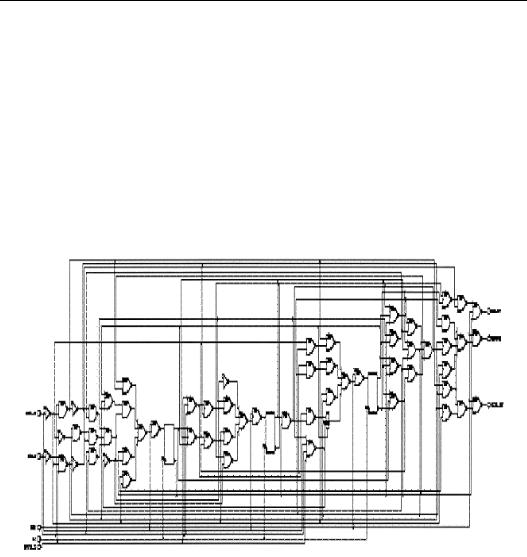
Figure A-15 Soft Drink Machine—Count Nickels Version
Schematic
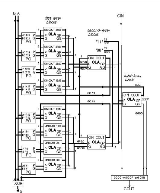
Carry-Lookahead Adder
This example of a carry-lookahead adder uses concurrent procedure calls to build a 32-bit carry-lookahead adder. The adder is built by
A-42 |
Xilinx Development System |

Examples
partitioning of the 32-bit input into eight slices of 4 bits each. Each of the eight slices computes propagate and generate values by using the PG procedure.
Propagate (output P from PG) is ’1’ for a bit position if that position propagates a carry from the next-lower position to the next-higher position. Generate (output G) is ’1’ for a bit position if that position generates a carry to the next-higher position, regardless of the carryin from the next lower position. The carry-lookahead logic reads the carry-in, propagate, and generate information computed from the inputs. The logic computes the carry value for each bit position and makes the addition operation an XOR of the inputs and the carry values.
Carry Value Computations
The carry values are computed by a three-level tree of 4-bit carrylookahead blocks.
•The first level of the tree computes the 32 carry values and the eight group-propagate and generate values. Each of the first-level group-propagate and generate values tells if that 4-bit slice propagates and generates carry values from the next-lower group to the next-higher group. The first-level lookahead blocks read the group carry computed at the second level.
•The second-level lookahead blocks read the group-propagate and generate information from the four first-level blocks and then compute their own group-propagate and generate information. The second-level lookahead blocks also read group carry information computed at the third level to compute the carries for each of the third-level blocks.
•The third-level block reads the propagate and generate information of the second level to compute a propagate and generate value for the entire adder. It also reads the external carry to compute each second-level carry. The carry-out for the adder is ’1’ if the third-level generate is ’1’ or if the third-level propagate is ’1’ and the external carry is ’1’.
The third-level carry-lookahead block is capable of processing four second-level blocks. But because there are only two secondlevel blocks, the high-order 2 bits of the computed carry are ignored; the high-order two bits of the generate input to the
VHDL Reference Guide |
A-43 |

VHDL Reference Guide
third-level are set to zero, ”00”; and the propagate high-order bits are set to ”11”. These settings cause the unused portion to propagate carries but not to generate them. The following figure shows the overall structure for the carry-lookahead adder.
A-44 |
Xilinx Development System |
Examples
Figure A-16 Carry-Lookahead Adder Block Diagram
VHDL Reference Guide |
A-45 |

VHDL Reference Guide
The VHDL implementation of the design in the previous figure is accomplished with four procedures:
•CLA—Names a 4-bit carry-lookahead block.
•PG—Computes first-level propagate and generate information.
•SUM—Computes the sum by adding the XOR values to the inputs with the carry values computed by CLA.
•BITSLICE—Collects the first-level CLA blocks, the PG computations, and the SUM. This procedure performs all the work for a 4- bit value except for the secondand third-level lookaheads.
The following example shows a VHDL description of the adder.
package LOCAL is
constant N: INTEGER := 4;
procedure BITSLICE(
A, B: in BIT_VECTOR(3 downto 0); CIN: in BIT;
signal S: out BIT_VECTOR(3 downto 0); signal GP, GG: out BIT);
procedure PG(
A, B: in BIT_VECTOR(3 downto 0); P, G: out BIT_VECTOR(3 downto 0));
function SUM(A, B, C: BIT_VECTOR(3 downto 0)) return BIT_VECTOR;
procedure CLA(
P, G: in BIT_VECTOR(3 downto 0); CIN: in BIT;
C: out BIT_VECTOR(3 downto 0); signal GP, GG: out BIT);
end LOCAL;
package body LOCAL is
-----------------------------------------------
-- Compute sum and group outputs from a, b, cin
-----------------------------------------------
procedure BITSLICE(
A, B: in BIT_VECTOR(3 downto 0); CIN: in BIT;
signal S: out BIT_VECTOR(3 downto 0); signal GP, GG: out BIT) is
variable P, G, C: BIT_VECTOR(3 downto 0); begin
PG(A, B, P, G);
A-46 |
Xilinx Development System |
Examples
CLA(P, G, CIN, C, GP, GG); S <= SUM(A, B, C);
end;
----------------------------------------------------
-- Compute propagate and generate from input bits
----------------------------------------------------
procedure PG(A, B: in BIT_VECTOR(3 downto 0);
P, G: out BIT_VECTOR(3 downto 0)) is
begin
P <= A or B; G <= A and B;
end;
----------------------------------------------------
-- Compute sum from the input bits and the carries
----------------------------------------------------
function SUM(A, B, C: BIT_VECTOR(3 downto 0)) return BIT_VECTOR is
begin
return(A xor B xor C); end;
--------------------------------
-- 4-bit carry-lookahead block
--------------------------------
procedure CLA(
P, G: in BIT_VECTOR(3 downto 0); CIN: in BIT;
C: out BIT_VECTOR(3 downto 0); signal GP, GG: out BIT) is
variable TEMP_GP, TEMP_GG, LAST_C: BIT; begin
TEMP_GP <= P(0);
TEMP_GG <= G(0); LAST_C <= CIN; C(0) <= CIN;
for I in 1 to N-1 loop TEMP_GP <= TEMP_GP and P(I);
TEMP_GG <= (TEMP_GG and P(I)) or G(I); LAST_C <= (LAST_C and P(I-1)) or G(I-1); C(I) <= LAST_C;
end loop;
VHDL Reference Guide |
A-47 |

VHDL Reference Guide
GP <= TEMP_GP; GG <= TEMP_GG;
end;
end LOCAL;
use WORK.LOCAL.ALL;
---------------------------------
-- A 32-bit carry-lookahead adder
---------------------------------
entity ADDER is
port(A, B: in BIT_VECTOR(31 downto 0); CIN: in BIT;
S: out BIT_VECTOR(31 downto 0); COUT: out BIT);
end ADDER;
architecture BEHAVIOR of ADDER is
signal GG,GP,GC: BIT_VECTOR(7 downto 0);
--First-level generate, propagate, carry signal GGG, GGP, GGC: BIT_VECTOR(3 downto 0);
--Second-level gen, prop, carry
signal GGGG, GGGP: BIT;
-- Third-level gen, prop
begin
--Compute Sum and 1st-level Generate and Propagate
--Use input data and the 1st-level Carries computed
--later.
BITSLICE(A( 3 downto 0),B( 3 downto 0),GC(0),
S( 3 downto 0),GP(0), GG(0));
BITSLICE(A( 7 downto 4),B( 7 downto 4),GC(1),
S( 7 downto 4),GP(1), GG(1));
BITSLICE(A(11 downto 8),B(11 downto 8),GC(2),
S(11 downto 8),GP(2), GG(2));
BITSLICE(A(15 downto 12),B(15 downto 12),GC(3),
S(15 downto 12),GP(3), GG(3));
BITSLICE(A(19 downto 16),B(19 downto 16),GC(4),
S(19 downto 16),GP(4), GG(4));
BITSLICE(A(23 downto 20),B(23 downto 20),GC(5),
S(23 downto 20),GP(5), GG(5));
BITSLICE(A(27 downto 24),B(27 downto 24),GC(6),
S(27 downto 24),GP(6), GG(6));
BITSLICE(A(31 downto 28),B(31 downto 28),GC(7),
S(31 downto 28),GP(7), GG(7));
A-48 |
Xilinx Development System |