

Fiber_Optics_Physics_Technology
.pdf8.8. Optical Amplifiers |
135 |
Let us now continue our gedanken experiment and place an ideal detector at the output of the ideal amplifier. “Ideal” means that it can detect photons such that the equality is fulfilled in the uncertainty relation:
nout |
φout = |
1 |
. |
2 |
|||
The detector will thus register nout ± |
nout photons and a phase of φout ± φout. |
||
There is no reason why it should be wrong to think of the combination of amplifier and detector as one unit, which would serve as a particularly sensitive detector. This internal-gain detector then measures a signal with
1 nin φin = 2G ,
which violates the uncertainty relation whenever the amplifier deserves its name, i.e., whenever G > 1.
The contradiction is resolved when one accepts the following: Any amplifier adds as much noise to a signal with frequency ν as a hypothetical noise source at the amplifier input would when the amplifier were ideal, and the noise source had a spectral power density of
dP |
|
1 |
|
|
|
= |
1 − |
|
hν . |
dν |
G |
|||
This immediately shows: the only possible noise-free amplifier has G = 1 in which case the word amplifier would be a misnomer.
What does this mean? One might na¨ıvely think that an attenuation of some signal and subsequent amplification by the same factor would faithfully reconstitute the original signal. This is not so! There will be an additional noise contribution. This extra noise may be strong if the amplifier is of mediocre engineering, but even the best amplifiers will always add at least some noise. Fortunately, engineering of optical amplifiers has matured so far that the best commercially available types are extremely close to the theoretical limit.
For a practical realization of optical amplifiers, there are two quite di erent approaches or technologies: active fibers and semiconductor elements.
8.8.1Amplifiers Involving Active Fibers
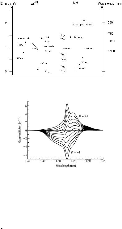
It seems that the interest is shifting toward amplifiers which consist simply of a piece of special fiber. Amplifying fiber is doped with suitable materials and receives power from an auxiliary light source. In the third transmission window, erbium is the most suitable dopant [23]; at several other wavelengths, useful dopants are also known, like neodymium at 1.06 μm. Figure 8.18 schematically shows the relevant energy levels of these substances. When the transition at 980 or 1,480 nm is pumped, an inversion of the 4I13/2 with respect to the 4I15/2 ground state is created; this implies an optical gain. With a few tens of milliwatts pump power, one can achieve 30 dB gain in about 10 m of erbium-doped fiber. The gain bandwidth extends from 1, 530 to 1, 570 nm (Fig. 8.19). The lifetime of the upper state is extremely long (10 ms), and therefore gain saturation and thus channel crosstalk among wavelength channels are practically absent. This is important because otherwise the huge bandwidth would not be useable.
136 |
|
Chapter 8. Components for Fiber Technology |
||||
( ) |
|
|
|
|
|
( ) |
|
||||||
|
|
|
|
|
|
|
|
|
|
|
|
|
|
|
|
|
|
|
|
|
|
|
|
|
|
|
|
|
|
|
|
|
|
|
|
|
|
|
|
|
u |
|
, |
|
|
|
|
|
||
|
|
|
|
|
|
|
|
|
|
|
|
|
|
|
|
|
|
|||||
|
|
|
|
|
|
|
|
|
|
|
|
|
|
|
|
|
|
|
|
|
|
|
|
|
|
|
|
|
|
|
|
|
|
|
|
|
|
|
|
|
|
|
|
|
|
|
|
|
|
|
|
|
|
|
|
|
|
|
|
r |
|
|
|
|
|
, |
||
|
|
|
|
r |
|
|
|
u |
|
|
|
, |
|
|
|
|
|
|||||
, |
|
|
|
|
|
|
|
|
|
|
|
|
|
, |
||||||||
|
|
|
|
|
||||||||||||||||||
|
|
|
|
|
|
|
|
|
|
|
|
|
|
|
|
|
|
|||||
|
|
|
|
|
|
|
|
|
|
|
|
|
|
|
|
|
|
|||||
|
|
|
|
|
|
|
|
|
|
|
|
|
|
|
|
|
|
|
|
|
|
|
|
|
|
|
|
|
|
|
|
|
|
|
|
|
|
|
|
|
|
|
|
|
|
|
|
|
|
|
|
|
|
|
|
|
|
|
|
|
|
|
|
|
|
|
|
|
|
|
|
|
|
|
|
|
|
|
|
|
|
|
|
|
|
|
|
|
|
|
|
|
|
|
|
|
|
|
, |
|
|
|
|
|
|
|
, |
|
|
|
|
|
|
|
|
|
|
|
|
|
|
|
|
|
|
|
|
|
|
|
|
|
|
|
|
|
|
|
|
|
|
|
|
|
|
|
|
|
|
|
|
|
|
|
|
|
|
|
|
|
|
|
|
|
|
|
|
|
|
|
|
|
|
|
|
|
|
|
|
|
|
|
|
|
|
|
|
|
|
|
|
|
|
|
|
|
|
|
|
|
|
|
|
|
|
|
|
|
|
|
|
|
|
|
|
|
|
|
|
|
|
|
|
|
|
|
|
|
|
Figure 8.18: Level scheme for optical fibers doped with Er ions or Nd ions. Shown are the energetic levels in electron volts and the transition wavelengths in nanometers, both referred to the ground state.
Figure 8.19: Gain spectrum of an Er-doped fiber for various levels of inversion. Without any inversion (bottom curve) the fiber absorbs light. As the inversion increases, gain first appears at the long-wavelength side. At the highest inversion shown (top curve), the gain has spread across the entire band. From [40].
While the gain is not flat throughout the gain bandwidth, it can be equalized to a large extent with filters.
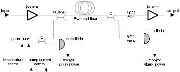
The complete setup of an Er-doped fiber amplifier has the following components (Fig. 8.20):
a pump source, typically a continuous-wave laser diode with high power (on the order of 100 mW) at 980 or 1,480 nm;
8.8. Optical Amplifiers |
137 |
||||||||||||||||||||
|
|
|
|
|
|
|
|
|
|
|
|
|
|
|
|
|
|
|
|
|
|
|
|
|
|
|
|
|
|
|
|
|
|
|
|
|
|
|
|
|
|
|
|
|
|
|
|
|
|
|
|
|
|
|
|
|
|
|
|
|
|
|
|
|
|
|
|
|
|
|
|
|
|
|
|
|
|
|
|
|
|
|
|
|
|
|
|
|
|
|
|
|
|
|
|
|
|
|
|
|
|
|
|
|
|
|
|
|
|
|
|
|
|
|
|
|
|
|
|
|
|
|
|
|
|
|
|
|
|
|
|
|
|
|
|
|
|
|
|
|
|
|
|
|
|
|
|
|
|
|
|
|
|
|
|
|
|
|
|
|
|
|
|
|
|
|
|
|
|
|
|
|
|
|
|
|
|
|
|
|
|
|
|
|
|
|
|
|
|
|
|
|
|
|
|
|
|
|
|
|
|
|
|
|
|
|
|
|
|
|
|
|
|
|
|
|
|
|
|
|
|
|
|
|
|
|
|
|
|
|
|
|
|
|
|
|
|
|
|
|
|
|
|
|
|
|
|
|
|
|
|
|
|
|
|
|
|
|
|
|
|
|
|
|
|
|
|
|
|
|
|
|
|
|
|
|
|
|
|
|
|
|
|
|
|
|
|
|
|
|
|
|
|
|
|
|
|
|
|
|
|
|
|
|
|
|
|
|
|
|
|
|
|
|
|
|
|
|
|
|
|
|
|
|
|
|
|
|
|
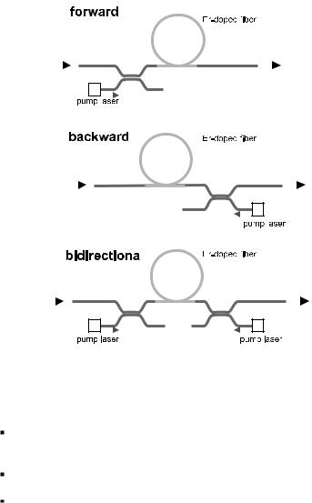
Figure 8.20: Various possibilities to employ an Er-doped fiber amplifier: forward pumping, backward pumping, and bidirectional pumping.
a wavelength-dependent coupler which inserts the pump light into the signal path;
a suitable length of Er-doped fiber; and
optical isolators which block backtraveling light and therefore make sure that both amplification of spontaneous emission in backward direction and stimulated Brillouin scattering (see Sect. 9.7.1) are suppressed.
A typical setup is shown in Fig. 8.21. Such amplifiers are o ered commercially. They can be employed in a variety of ways:
As booster: for postamplification of a low-power light source at the beginning of a transmission line.
As intermediate amplifier: for compensation of loss inserted somewhere along the line.
As preamplifier: to increase the sensitivity of photodetectors for weak signals at the end of a transmission line.
138 |
|
|
|
|
|
|
|
|
|
|
|
|
|
|
|
|
Chapter 8. Components for Fiber Technology |
||||||||||
|
|
|
|
|
|
|
|
|
|
|
|
|
|
|
|
|
|
|
|
|
|
|
|
|
|
|
|
|
|
|
|
|
|
|
|
|
|
|
|
|
|
|
|
|
|
|
|
|
|
|
|
|
|
|
|
|
|
|
|
|
|
|
|
|
|
|
|
|
|
|
|
|
|
|
|
|
|
|
|
|
|
|
|
|
|
|
|
|
|
|
|
|
|
|
|
|
|
|
|
|
|
|
|
|
|
|
|
|
|
|
|
|
|
|
|
|
|
|
|
|
|
|
|
|
|
|
|
|
|
|
|
|
|
|
|
|
|
|
|
|
|
|
|
|
|
|
|
|
|
|
|
|
|
|
|
|
|
|
|
|
|
|
|
|
|
|
|
|
|
|
|
|
|
|
|
|
|
|
|
|
|
|
|
|
|
|
|
|
|
|
|
|
|
|
|
|
|
|
|
|
|
|
|
|
|
|
|
|
|
|
|
|
|
|
|
|
|
|
|
|
|
|
|
|
|
|
|
|
|
|
|
|
|
|
|
|
|
|
|
|
|
|
|
|
|
|
|
|
|
|
|
|
|
|
|
|
|
|
|
|
|
|
|
|
|
|
|
|
|
|
|
|
|
|
|
|
|
|
|
|
|
|
|
|
|
|
|
|
|
|
|
|
|
|
|
|
|
|
|
|
|
|
|
|
|
|
|
|
|
|
|
|
|
|
|
|
|
|
|
|
|
|
|
|
|
|
|
|
|
|
|
|
|
|
|
|
|
|
|
|
|
|
|
|
|
|
|
|
|
|
|
|
|
|
|
|
|
|
|
|
|
|
|
|
|
|
|
|
|
|
|
|
|
|
|
|
|
|
|
|
|
|
|
|
|
|
|
|
|
|
|
|
|
|
|
|
|
|
|
|
|
|
|
|
|
|
|
|
|
|
|
|
|
|
|
|
|
|
|
|
|
|
|
|
|
|
|
|
|
|
|
|
|
|
|
|
|
|
|
|
|
|
|
|
|
|
|
Figure 8.21: Setup of a realistic Er-doped fiber amplifier in forward-pumping geometry. C: coupler (tap, e.g., 95:5 coupler), WDM-C: wavelength-dependent coupler to separate signal and pump wavelengths. Filter ASE: selective filter to suppress amplified spontaneous emission. Filter pump: selective filter to suppress pump light.
As distribution amplifier: for compensation of losses where the signal power is split into several branches, to restore the original power level in all branches.
As an oscillator: by optical feedback, the amplifier is turned into a laser (typically in conjunction with wavelength-tuning elements). We note that a fiber amplifier with an optical resonator to provide feedback operates as a fiber laser; we will return to this aspect in Sect. 8.9.4.
In the second window neodymium or praseodymium is used to dope the fibers. They do not make quite as near-perfect amplifiers as erbium does, but there is a large volume of installed fiber-optic systems operating in the second window, and therefore there is considerable interest in making amplifiers for this wavelength regime.
8.8.2Amplifiers Involving Semiconductor Devices
In suitable semiconductor materials with a p–n junction one can excite carriers from the valence band into the conduction band by running an electric current through the junction (see Sect. 8.9.1 below). The current thus produces an inversion, a nonequilibrium excess population in a higher-energy state. The excited carriers can then return to the valence band by emission of a photon. When this return is triggered (“stimulated”) by a signal photon, the process constitutes an amplification. The mechanism is also central for the operation of semiconductor lasers (see below).
If a laser diode is operated without optical feedback, it never reaches the threshold for laser oscillation and functions as an amplifier: Stimulated emission amplifies light sent in. Advantages of this technology are that devices are readily available, and the energy supply could not be any simpler. Disadvantages are the relatively narrow gain bandwidth and the less-than-perfect linearity of the amplification. If several wavelength channels are used simultaneously, the inversion gets modulated with the beat frequency. Then one finds a possibly quite severe channel crosstalk. The more wavelength channels are used, the

8.9. Light Sources |
139 |
more serious the problems get. This is why semiconductor amplifiers have not found quite the same acceptance in practical applications as doped-fiber devices.
8.9Light Sources
There is a vast variety of light sources known to man. Discounting sun and stars as well as flames, we name just a few:
Tungsten filament light bulbs
Bulk lasers
Luminescent diodes (LEDs)
Laser diodes
Fiber lasers
For fiber technology, there are certain demands which a light source must meet:
Must be possible to couple into fiber with good e ciency
Must have low energy requirements
Must be cost-e ective
Must have long lifetime
Must be virtually maintenance-free
Must provide means of modulation
The first five items are based on economic considerations because one has to expect that in a vast fiber network there may be huge numbers of light sources, many of which are located in far-flung and hard-to-reach places. Modulation is a requirement dictated immediately by the application: to transmit information.
Of course, light bulbs are ruled out. Their coupling e ciency is minimal, their lifetime is inadequate, and their capability for modulation exists only for frequencies up to a few hertz, certainly not gigahertz. Bulk lasers as found in many physics laboratories (think He-Ne lasers, Nd:YAG lasers, etc.) have good spatial coherence and thus good coupling e ciency. On the other hand, cost, energy, and maintenance requirements are definite disadvantages for any application outside a research lab and so is the lack of modulation capability at least in most types.
Therefore, from the above list, only luminescent diodes (LEDs), laser diodes, and fiber lasers are left as viable light sources. We will now discuss these choices in somewhat more detail.
8.9.1Light from Semiconductors
The mechanism of light generation in semiconductors is the recombination of carriers at a p–n junction. An electric current provides the energy required to excite electrons to the conduction band; as they relax back to the valence band, the amount of energy corresponding to the band gap is released in form of a photon. For a semiconductor with band gap Egap, one finds light with a frequency of ν ≈ Egap/h.
140 |
Chapter 8. Components for Fiber Technology |
8.9.2Luminescent Diodes
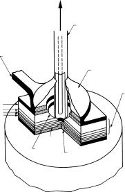
The recombination radiation has, without extra steps, no preference for any particular spatial direction. In LEDs, one does not attempt to achieve much directionality other than getting the light out of the component on one side, typically in a wide cone. LEDs perfectly fulfill the above requirements of low cost, low power operation, and long lifetime without maintenance. They can be modulated up to perhaps 100 MHz, which is su cient for many applications. However, for fundamental reasons the fiber-coupling e ciency is not impressive, and the power actually launched into a fiber is low, well under 1 mW. In this situation, LEDs find applications for short distances, like in LANs (local area networks) within premises where highest data rates are less important than lowest cost. With certain geometries, it has been attempted to optimize the coupling e ciency. Figure 8.22 shows the design of a “Burrus LED” where the fiber is butt-coupled to the light-emitting chip.
|
Fiber |
|
Metal |
|
|
contacting |
|
|
tab |
|
Mechanical |
|
|
alignment/support |
|
|
structure |
|
|
50 micrometer |
GaAs (n) |
|
thick |
|
AlGaAs double |
|
AlGaAs (n) |
|
|
|
heterostructure |
|
GaAs (p) |
|
|
AlGaAs (p) |
|
material |
GaAs (p) |
|
|
Oxide |
|
|
Etched |
Metal |
|
“well” |
|
|
contact |
|
|
|
|
|
STUD |
|
|
Figure 8.22: Construction of a “Burrus LED.” The fiber is butt-coupled to the light-emitting chip and is permanently held in place to avoid the need of later adjustment.
8.9.3Laser Diodes
The same principle of generation of light can be refined into the concept of laser diodes. One shapes the semiconductor chip in such a way that optical feedback is obtained. Then a stimulated process takes over, and coherent emission of light results. Coherent light is tremendously much easier to focus and couple into a fiber than incoherent light.
The first laser diodes in the 1960s consisted of little more than a semiconductor chip with p-doped and n-doped material. They had smoothly cleaved end facets with a natural reflectivity (Fresnel reflection) on the order of 30%, due to the high refractive index of semiconductors like GaAs of about n = 3
8.9. Light Sources |
141 |
|||
|
|
|
|
|
|
|
|
|
|
|
|
|
|
|
Figure 8.23: A schematic view of a laser diode. This simplest of all structures is known as broad area structure because the active (gain) region is very wide. It allows a large number of transverse modes to oscillate.
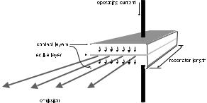
(Fig. 8.23). This reflectivity is fully su cient for resonator mirrors. The side faces of the chip remain unpolished and rough and are therefore no good reflectors. The length of the chip on the order of 300 μm is basically defined by the required gain length. The thickness of the active layer is on the order of 0.5 μm. These dimensions have immediate consequences for the modal structure of the laser resonator.
The resonator is hundreds of wavelengths long. Then the frequencies of adjacent longitudinal modes di er by fractions of 1%. As the gain bandwidth amounts to several percent of the central frequency, one can expect the simultaneous oscillation of several longitudinal modes. In some cases that may even be desirable: The process of mode locking can be used to generate short pulses of light. As for transverse modes, the active layer is thin; in the direction perpendicular to the active layer only a single mode can oscillate. On the other hand, in the lateral direction (perpendicular to the optical axis and parallel to the active layer), there is a 100 μm or so wide gain structure which gives rise to a multiplicity of lateral modes. Moreover, the modal structure in operation will not be constant during operation because both carrier density and temperature (heating during operation) will a ect the refractive index. Consider places where a particular oscillating mode depletes the inversion: Here the refractive index will be reduced, and the gain mechanism will then prefer other modes. One therefore has to expect undesired sudden changes in the modal structure (mode hops) during operation.
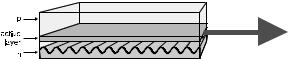
Gain Guiding
In view of these problems it was a first improvement to modify the geometry of current flow through the chip. Narrow contact stripes, or the introduction of insulating zones, make it possible to restrict the current flow to a narrow region in the active layer which may be just a couple of micrometers wide. This is shown schematically in Fig. 8.24. Gain occurs only where there is su cient current density which is now only a small part of the active layer; this is called a gain-guided geometry. The advantages are that (i) the current density is increased in the relevant position which lowers the laser threshold and (ii) the transverse mode profile is strongly restricted. Nevertheless, mode hops are not entirely eliminated; this is easily seen in kinks of the output power vs. pump current characteristics of such lasers. When it comes to coupling light from such
142 |
|
|
Chapter 8. Components for Fiber Technology |
|||||
|
|
|
|
|
|
|
|
|
|
|
|
|
|
|
|
|
|
|
|
|
|
|
|
|
|
|
|
|
|
|
|
|
|
|
|
|
|
|
|
|
|
|
|
|
|
|
|
|
|
|
|
|
|
|
|
|
|
|
|
|
|
|
Figure 8.24: Possible structure of a gain-guided laser diode. Oxide layers restrict the electrical contacts, and thus the current flow, to a narrow zone. Carriers are injected into the active zone only where su cient current density exists. The resulting rise in refractive index guides the light and restricts the emission to basically the same narrow zone.
lasers into fibers, there are nasty consequences: Changes in the modal structure give rise to modified overlap with the fiber’s modal profile and result in jumps of the incoupled power. Unpredictable severe fluctuations of power are certainly not desirable for any application.
Index Guiding
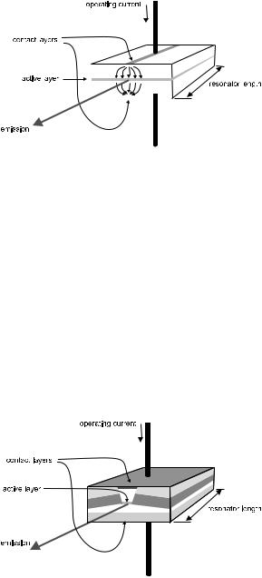
The next improvement was the introduction of the index-guided laser diode geometry. In a considerably more involved production process (which, however, has become routine now), there are lateral steps of the refractive index built into the active layer by use of di erently doped material. This is shown in Fig. 8.25.
Figure 8.25: Possible structure of an index-guided laser diode. The active zone is surrounded on all sides by material with larger band gap; this is also known as “buried heterostructure.” A lateral index step of ≈0.2 provides strong guidance of the light. By way of the intricate structure, it is assured that also the current flows only through the relevant part of the active zone, resulting in a low laser threshold. Many di erent geometries of buried heterostructure lasers have been suggested and realized; the one shown here is called an “etched-mesa” structure.
8.9. Light Sources |
143 |
Even weak index guiding with index steps on the order of 1% make sure that the index modifications through the concentration of carriers are overwhelmed. Therefore these structures can run in lateral single-mode operation.
Distributed Feedback
Finally let us look at the longitudinal modes. As long as the resonator mirrors at the chip facets set the mode spacing, there is little one can do to achieve single-mode operation: One cannot make the chip shorter because a certain length is required to provide adequate gain. In this situation only frequencyselective means can help. When longitudinal single-mode operation is required, one uses laser diodes into which a grating has been incorporated for wavelength selectivity (see Fig. 8.26). The grating favors feedback at the frequencies defined by a Bragg condition for the grating. One can obtain both the selection of a single mode and an improved frequency stability of this particular mode. The grating may be extended over the entire resonator length; then this is known as distributed feedback or DFB laser. The grating may alternatively be formed only on short segments toward the resonator ends in a zone with little gain; this is then called distributed Bragg reflector or DBR laser. Both DFB and DBR lasers have become something of a standard for long-haul transmission because single-mode operation is favorable, and the frequency stability is good.
Figure 8.26: Schematic representation of a distributed feedback laser (DFB laser). A periodic index modulation is introduced over the entire resonator length; it acts as a grating and selects a particular frequency.
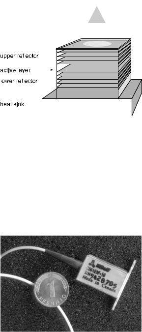
VCSELs
In a more recent development laser diodes are also made with an entirely di erent geometry: They are called vertical cavity surface emitting lasers or VCSELs (rhymes with pixels; see Fig. 8.27). In these lasers, the light does not travel the length but the width of the active layer. This implies that the optical axis (the direction of light propagation) is parallel to the direction of the pump current. Above and below the active layer, there are multiple layer reflectors acting as wavelength-selective mirrors similar to a DBR structure. In this concept, the resonator length is very short – hardly any longer than the wavelength. This enforces longitudinal single-mode operation, which is a definite advantage. The lateral beam profile can be optimized by suitable structuring. In fact, meanwhile VCSELs can produce better beam geometries than side-emitting lasers. A downside is that since their resonator and thus their gain length are so short, it has been di cult to generate high output powers from VCSELs. On the other hand, they can be modulated at high speed (well above 10 GHz instead of a few gigahertz). By this token, it appears likely that they will find applications in fiber optics.
Laser diodes provide the best combination of properties of lasers (spatial coherence assures good incoupling e ciency) with those of LEDs: long lifetime
144 |
|
|
|
|
|
|
Chapter 8. Components for Fiber Technology |
|||||
|
|
|
|
|
|
|
|
|
|
|
|
|
|
|
|
|
|
|
|
|
|
|
|
|
|
|
|
|
|
|
|
|
|
|
|
|
|
|
|
|
|
|
|
|
|
|
|
|
|
|
|
|
|
|
|
|
|
|
|
|
|
|
|
|
|
|
|
|
|
|
|
|
|
|
|
|
|
|
|
|
|
|
|
|
|
|
|
|
|
|
|
|
|
|
|
|
|
|
|
|
|
|
|
|
|
|
|
|
|
|
|
|
|
|
|
|
|
|
|
|
|
|
|
|
|
|
|
|
|
|
|
|
|
|
|
|
|
|
|
|
|
|
|
|
|
|
|
|
|
|
|
|
|
|
|
|
|
|
|
|
|
|
|
|
|
|
|
|
|
|
|
|
|
|
|
|
|
|
|
|
|
|
|
|
|
|
|
|
|
|
|
|
|
|
Figure 8.27: Schematic representation of a VCSEL. In this figure, the vertical dimensions are exaggerated for the sake of clarity. Bragg reflectors above and below the active layer provide feedback; the thickness of the active layer is only one wavelength or so.
and low operational power requirement. They can be modulated into the gigahertz regime, which is often good enough; if not, they are operated continuous wave, and an external modulator serves to carve out pulses as required. Cost ranges from just a few euros for the simplest types up to a few thousand euros, for the fanciest DFB lasers and other specialty constructions; however, in relation to the complete system this may still be considered low cost. All told, laser diodes fulfill all the important requirements of fiber technology and are therefore the de facto standard. Figure 8.28 shows a typical laser diode. The
Figure 8.28: A laser diode made for communication purposes. This device is enclosed in a housing which must be bolted to a heat sink with the flange visible on the right, in order to remove heat. The electrical connections are by pins on the bottom and are not visible in this picture. The optical output goes into a piece of fiber attached to the laser (the pigtail). The pigtail is protected with a plastic coating and a rubber bend relief where it leaves the case.