

Biomolecular Sensing Processing and Analysis - Rashid Bashir and Steve Wereley
.pdfIMPLANTABLE WIRELESS MICROSYSTEMS |
217 |
REFERENCE
ELECTRODE
RECEIVING
COIL (ANTENNA)
HYBRID CHARGE
STORAGE
CHIP CAPACITOR
GLASS
CAPSULE
PACKAGE HYBRID CMOS AND BIPOLAR
INTEGRATED CIRCUIT CHIP
SILICON
SUBSTRATE
STIMULATING
ELECTRODE
FIGURE 10.10. Schematic of a single channel implantable neuromuscular microstimulator.
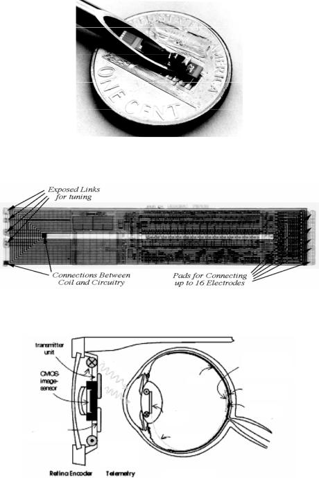
electrodes located at the ends of a silicon substrate. A hybrid capacitor is used to store the charge in between the stimulation pulses and to deliver 10 mA of current to the muscle every 25 msec. A glass capsule hermetically seals a BiCMOS receiver circuitry along with various other passive components (receiver coil and charge storage capacitor) located on top of the silicon substrate. Figure 10.11 shows a photograph of the microstimulator in the bore of a gauge 10 hypodermic needle. As can be seen, the device requires a complicated hybrid assembly process in order to attach a wire-wound coil and a charge storage capacitor to the receiver chip. In a subsequent design targeted for direct peripheral nerve stimulation (requiring smaller stimulation current), the coil was integrated on top of the BiCMOS electronics and on-chip charge storage capacitors were used thus considerably simplifying the packaging process. Figure 10.12 shows a micrograph of the chip with the electroplated copper inductor [57].
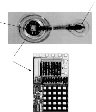
Figure 10.13 shows the schematic of the visual prosthetic microsystem [46]. A spectacle mounted camera is used to capture the visual information followed by digital conversion and transmission of data to a receiver chip implanted in the eye. The receiver uses this information to stimulate the ganglion cells in the retina through a microelectrode array in sub or epi-retinal location. This microsystem is designed for patients suffering from macular degeneration or retinitis pigmentosa. In both diseases the light sensitive retinal cells (cones and rods) are destroyed while the more superficial retinal cells, i.e., ganglion cells, are still viable and can be stimulated. Considering that macular degeneration is an
218 |
BABAK ZIAIE |
FIGURE 10.11. Photograph of the microstimulator in the bore of a gage 10 hypodermic needle.
FIGURE 10.12. Microstimulator chip with integrated receiver coil and on-chip storage capacitor [57].
transmitter |
|
||
|
unit |
signal/power |
|
|
|
|
|
|
CMOS |
|
|
|
|
|
|
|
image- |
|
|
|
sensor |
|
|
neural signal processor
FF/ optoelectronic transmission
Retina Encoder |
|
Telemetry |
encapsulated stimulator-chip
(flexible silicon chip)
retina
microelectrode array
stimulation receiver circuitry
unit
microcable
RetinaStimulator
FIGURE 10.13. Schematic of a visual prosthetic microsystem [46].
IMPLANTABLE WIRELESS MICROSYSTEMS |
219 |
Stimulating
Electrodes
Antenna
Receiver Chip
FIGURE 10.14. Retinal stimulator receiver chip, stimulating electrodes, and polyimide antenna [46].
age related pathology and will be afflicting more and more people as the average age of the population increases, such a microsystem will be of immense value in the coming decades. There are several groups pursuing such a device with different approaches to electrode placement (epi or sub retinal), chip design, and packaging. A German consortium which has also designed the IOP measurement microsystem is using a similar approach in antenna placement (receiver antenna in the lens), chip design, and packaging technology to implement a retinal prosthesis [46]. Figure 10.14 shows photographs of the retinal stimulator receiver chip, stimulating electrodes, and polyimide antenna. The effort in the United States is moving along a similar approach [58, 59].
10.6. CONCLUSIONS AND FUTURE DIRECTIONS
In this article, we reviewed several implantable wireless microsystems currently being developed in the academia and industry. Recent advances in MEMS-based transducers, low-power CMOS integrated circuit, wireless communication transceivers, and advanced batch scale packaging have provided a unique opportunity to develop implantable wireless
220 |
BABAK ZIAIE |
microsystems with advanced functionalities not achievable previously. These microsystems will be indispensable to the 21st century physician by providing assistance in diagnosis and treatment. Future research and development will probably be focused on three areas: 1) nano-transducers, 2) self-assembly, and 3) advanced biomaterials. Although MEMSbased sensors and actuators have been successful in certain areas (particularly physical sensors), their performance could be further improved by utilizing nano-scale fabrication technology. This is particularly true in the area of chemical sensors where future diagnostic depends on detecting very small amounts of chemicals (usually biomarkers) well in advance of any physical sign. Nanosensors capable of high sensitivity chemical detection will be part of the future implantable microsystems. In the actuator/delivery area, drug delivery via nanoparticles is a burgeoning area which will undoubtedly be incorporated into future therapeutic microsystems. Future packaging technology will probably incorporate self-assembly techniques currently being pursued by many micro/nano research groups. This will be particularly important in microsystems incorporating multitude of nanosensors. Finally, advanced nano-based biomaterials will be used in implantable microsystems (wireless or not) in order to enhance biocompatibility and prevent biofouling. These will include biocompatible surface engineering and interactive interface design (e.g., surfaces that release anti-inflammatory drugs in order to reduce post implant fibrous capsule formation).
REFERENCES
[1]R.S. MacKay and B. Jacobson. Nature, 179:1239–1240, 1957.
[2]R.S. MacKay. Eng. Med. Biol. Mag., 2:11–17, 1983.
[3]J.W. Knutti, H.V. Allen, and J.D. Meindl. Eng. Med. Biol. Mag., 2:47–50, 1983.
[4]K.D. Wise (ed.). Proceedings of the IEEE, 86:1998.
[5]P.R. Troyk and M.A.K. Schwan. IEEE Transact. Biomed. Eng., 39:589–599, 1992.
[6]Z. Hamici, R. Itti, and J. Champier. Meas. Sci. Technol., 7:192–201, 1996.
[7]W.J. Heetderks. IEEE Trans. Biomed. Eng., 35:323–327, 1988.
[8]P.R. Gray and R.G. Meyer. Proceedings of the Custom Integrated Circuits Conference, pp. 83–89, 1995.
[9]A.A. Abidi. IEEE Microw. Mag., 4:47–60, 2003.
[10]W. Gopel, J. Hesse, and J.N. Zemel. Sensors: A Comprehensive Survey, Vols. 1–8, VCH Publishers, New York, 1989.
[11]J.M. Hohler and H.P. Sautz (ed.). Microsystem Technology: A Powerful Tool for Biomolecular Studies. Birkhauser, Boston, 1999.
[12]R.F. Taylor and J.S. Schultz. Handbook of Chemical and Biological Sensors. IOP Press, Bristol, 1996.
[13]E.K. Rogers (ed.). Handbook of Biosensors and Electronic Nose. CRC Press, Boca Raton, 1997.
[14]G.A. Hak (ed.). The MEMS Handbook. CRC Press, Boca Raton, 2001.
[15]M. Zhang, T. Desai, and M. Ferrari. Biomaterials, 19:953–960, 1998.
[16]D.W. Branch, B.C. Wheeler, G.J. Brewer, and D.E. Leckband. Biomaterials, 22:1035–1047, 2001.
[17]N.A. Alcantar, E.S. Aydil, and J.N. Israelachvili. J. Biomed. Mater. Res., 51:343–351, 2000.
[18]H. Baltes, O. Paul, and O. Brand. Proc. IEEE, 86:1660–1678, 1998.
[19]L.J. Stotts. IEEE Cir. Dev. Mag., 5:12–18, 1989.
[20]T. Stouraitis and V. Paliouras. IEEE Cir. Dev. Mag., 17:22–29, 2001.
[21]Y. Tsividis, N. Krishnapura,Y. Palakas, and L. Toth. IEEE Cir. Dev. Mag., 19:63–72, 2003.
[22]L. Benini, G. De Micheli, and E. Macii. IEEE Cir. Sys. Mag., 1:6–25, 2001.
[23]S.S. Rajput and S.S. Jamuar. IEEE Cir. Sys. Mag., 2:24–42, 2002.
[24]P. Troyk. Ann. Rev. Biomed. Eng., 1:177–209, 1999.
[25]B. Ziaie, M. Nardin, A.R. Coghlan, and K. Najafi. IEEE Trans. Biomed. Eng., 44:909–920, 1997.
[26]K. Finkenzeller. RFID Handbook, John Wiley, New York, 2003.
[27]J.G. Proakis and M. Salehi. Communication System Engineering. Pearson Education, 2001.
IMPLANTABLE WIRELESS MICROSYSTEMS |
221 |
[28]T.H. Lee. Design of CMOS Radiofrequency Integrated Circuits. Cambridge University Press, Cambridge, 1998.
[29]B. Razavi. IEEE Cir. Dev. Mag., 12:12–25, 1996.
[30]L.E. Larson. IEEE J. Solid-State Cir., 33:387–399, 1998.
[31]D. Linden and T. Reddy. Handbook of Batteries. McGraw-Hill, New York, 2001.
[32]K.R. Foster and H.P. Schwan. In C. Polk and E. Postow (eds.), Handbook of Biological Effects of Electromagnetic Fields. CRC Press, Boca Raton, 1996.
[33]W.H. Ko, S.P. Liang, and C.D.F. Fung. Med. Biol. Eng. Comput., 15:634–640, 1977.
[34]K.B. Ashby, I.A. Koullias,W.C. Finley, J.J. Bastek, and S. Moinian. IEEE J. Solid-State Cir., 31:4–9, 1996.
[35]N.O. Sokal and A.D. Sokal. IEEE J. Solid-State Cir., 10:168–176, 1975.
[36]B. Ziaie, S.C. Rose, M.D. Nardin, and K. Najafi. IEEE Trans. Biomed. Eng., 48:397–400, 2001.
[37]V. Mehta and J.S. Cooper. J. Power Sou., 114:32–53, 2003.
[38]D. Singh, R. Houriet, R. Giovannini, H. Hofmann, V. Craciun and R.K. Singh. J. Power Sou., 97–98:826–831, 2001.
[39]H. Guo and A. Lal. Proceeding of the Transducers Conference, pp. 36–39, 2003.
[40]T. Starner. IBM J. Sys., 35:618–629, 1996.
[41]B.D. Ratner, F.J. Schoen, A.S. Hoffman, and J.E. Lemons. Biomaterials Science: An Introduction to Materials in Medicine. Elsevier Books, New York, 1997.
[42]G.E. Loeb, M.J. Bak, M. Salcman, and E.M. Schmidt. IEEE Trans. Biomed. Eng., 24:121–128, 1977.
[43]M.F. Nichols. Critical Rev. Biomed. Eng., 22:39–67, 1994.
[44]M.A. Schmidt. Proc. IEEE, 86:1575–1585, 1998.
[45]B. Ziaie, J.A. Von Arx, M.R. Dokmeci, and K. Najafi. IEEE J. Microelectromech. Sys., 5:166–179, 1996.
[46]W. Mokwa and U. Schenakenberg. IEEE Trans. Instrument. Measure., 50:1551–1555, 2001.
[47]K. Stangel, S. Kolnsberg, D. Hammerschmidt, B.J. Hosticka, H.K. Trieu, and W. Mokwa. IEEE J. Solids-State Cir., 36:1094–1100, 2001.
[48]G. Iddan, G. Meron, A. Glukhovsky, and P. Swain. Nature, 405:417, 2000.
[49]D.G. Adler and C.J. Gostout. Hospital Physician, 14–22, 2003.
[50]http://www.givenimaging.com.
[51]http://www.rfnorika.com/.
[52]J.T. Santini, M.J. Cima, and R. Langer. Nature, 397:335–338, 1999.
[53]J.T. Santini, A.C. Richards, R. Scheidt, M.J. Cima, and R. Langer. Angewandte Chemie., 39:2396–2407, 2000.
[54]http://www.mchips.com.
[55]http://www.chiprx.com.
[56]M. Lei, A. Baldi, T. Pan, Y. Gu, R.A. Siegel, and B. Ziaie. Proc. IEEE MEMS, 391–394, 2004.
[57]J.A. Von Arx and K. Najafi. IEEE Solid-State Circuits Conference. pp. 15–17, 1999.
[58]W. Liu, E. McGucken, K. Vichienchom, S.M. Clements, S.C. Demarco, M. Humayun, E. de Juan, J. Weiland, and R. Greenberg. IEEE Systems, Man, and Cybernetics, Conference, pp. 364–369, 1999.
[59]M.S. Humayun, J. Weiland, B. Justus, C. Merrit, J. Whalen, D. Piyathaisere, S.J. Chen, E. Margalit, G. Fujii, R.J. Greenberg, E. de Juan, D. Scribner, and W. Liu. Proceedings of the 23rd Annual IEEE EMBS Conference. pp. 3422–3425, 2001.
11
Microfluidic Tectonics
J. Aura Gimm and David J. Beebe
Department of Biomedical Engineering, University of Wisconsin-Madison,
WI 53706
11.1. INTRODUCTION
Microfluidics has the potential to significantly change the way modern biology is performed. Microfluidic devices offer the ability to work with smaller reagent volumes, shorter reaction times, and the possibility of parallel operation. They also hold the promise of integrating an entire laboratory onto a single chip [23]. In addition to the traditional advantages conferred by miniaturization, the greatest potential lies in the physics of the scale. By understanding and leveraging micro scale phenomena, microfluidics can be used to perform techniques and experiments not possible on the macroscale allowing new functionality and experimental paradigms to emerge. Two examples of devices commonly considered microfluidic are gene chips and capillary electrophoresis. While gene chips take advantage of some of the benefits of miniaturization, they are not technically microfluidic devices. Chip-based capillary electrophoresis devices are now commercially available and reviews are available elsewhere [19, 28]. Certain fluid phenomena are dominant at the microscale and affect how devices can be made and used. Current techniques for making the devices will be outlined and examples will be given with an emphasis on a recently developed organic technology platform called microfluidic tectonics. Components of microdevices capable of actuating, sensing, and measuring within microfluidic systems will be discussed. Finally, complete systems that have been developed to perform functions in biology will be described.
*The research was generously funded by grants from DARPA-MTO (#F30602–00–1–0570)(Program manager: Dr. Michael Krihak).

224 J. AURA GIMM AND DAVID J. BEEBE
Target Application:
Chemical
Biological
Target market/user
|
b |
c |
Structural |
Sensing Components: |
|
Components: |
Shape-responsive |
|
Valves |
Colorimetric |
|
Pumps |
Cell-gel |
|
Filters |
Liposome |
|
Compartments |
Electrically-sensitive |
|
Mixers |
|
|
|
System Integration: |
|
|
Single vs. multiple layer |
|
|
System design |
|
|
External interface |
|
a
d
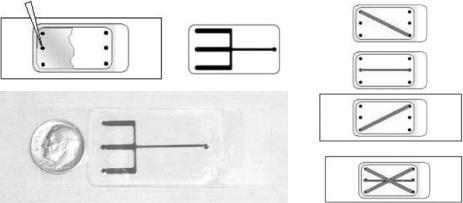
FIGURE 11.1. Microtectonic toolbox (a) and top view of layers fabricated for an integrated analysis system (d) where two separate layers (b, c) are connected through punched holes [59]. Channel width is 1 mm.
11.2. TRADITIONAL MANUFACTURING METHODS
The traditional techniques used for fabricating microfluidic devices include micromachining, embossing, and injection molding. Each technique has advantages and disadvantages and the most suitable method of device fabrication often depends on the specific application of the device [9].
11.2.1. Micromachining
Silicon micromachining is widely used in microelectromechanical systems (MEMS) and was one of the first techniques to be applied microfluidics. Complex systems can be manufactured out of silicon [49]. Recent advances in nanotechnology can also create nanometer structures for microfluidic applications [14]. Although micromachining techniques are widely used, silicon is often not the ideal material for microfluidic applications due to optical opacity, cost, difficulty in component integration, and surface characteristics that are not well suited for biological applications. The needs of many microfluidic applications do not require the precision that micromachining can offer. In addition, micromachining techniques are costly, labor intensive, and require highly specialized skills, equipment, and facilities. Silicon and glass based microfluidic devices are, however, well suited to some chemistry applications that require strong solvents, high temperatures, or chemically stable surfaces. Chip-based capillary electrophoresis is still largely the domain of glass machining because of the surface properties provided by glass.
11.2.2. Micromolding
Injection molding is a very promising technique for low cost fabrication of microfluidic device [18]. Thermoplastic polymer materials are heated past their glass transition
MICROFLUIDIC TECTONICS |
225 |
temperature to make them soft and pliable. The molten plastic is injected into a cavity that contains the master. Since the cavity is maintained at a lower temperature than the plastic, rapid cooling of the plastic occurs, and the molded part is ready in only a few minutes. The only time consuming step is creating the master that shapes the plastics. This master, often referred to as the molding tool, can be fabricated in several ways including metal micromachining, electroplating, and silicon micromachining. The methods of fabricating the molding tool are similar to those used for making the master for hot embossing and thus, the same issues of cost apply. However, the injection molding process is considerably faster than hot embossing and is the preferred method, from a cost perspective, for high volume manufacturing. Limitations of injection molding for microfluidics include resolution and materials choices.
11.3. POLYMERIC µFLUIDIC MANUFACTURING METHODS
11.3.1. Soft Lithography
In order to promote widespread use of microfluidic devices in biology, a faster, less expensive, and less specialized method for device fabrication was needed. Elastomeric micromolding was first developed at Bell Labs in 1974 when researchers developed a technique of molding a soft material from a lithographic master [5]. The concepts of soft lithography have been used to pattern surfaces via stamping and fabricate microchannels using molding and embossing. Several advances were made in Japan in the 1980s that demonstrated micromolded microchannels for use in biological experiments [51]. More recently, Whitesides [20, 52, 77] and others [36, 68] have revolutionized the way soft lithography is used in microfluidics.
Soft lithography typically refers to the molding of a two-part polymer (elastomer and curing agent), called polydimethylsiloxane (PDMS), using photoresist masters. A PDMS device has design features that are only limited by the master from which it is molded. Therefore, techniques used to create multidimensional masters using micromachining or photolithography can also be used to create complex masters to mold PDMS microstructures. A variety of complex devices have been fabricated, including ones with multidimensional layers [1, 46]. Soft lithography is faster, less expensive, and more suitable for most biological applications than glass or silicon micromachining. The application of soft lithography to biology is thoroughly reviewed elsewhere [77].
The term “soft lithography” can also be used to describe hot embossing techniques [27, 50]. Hot embossing usually refers to the transfer of a pattern from a micromachined quartz or metal master to a pliable plastic sheet. Typically, the polymer substrate and mastermold are heated separately under vacuum to an equal and uniform temperature higher than the glass transition temperature (Tg) of the polymer material. The master-mold is then pressed against the polymer substrate by a precisely controlled force. After a certain time the substrate and the mold are cooled to a temperature below the Tg while still applying the embossing force. The subsequent step of the process is deembossing, where the master-mold is separated from the substrate. During recent years a variety of microand nanostructures have been fabricated using hot embossing process [10, 34, 60, 71, 72]. The most commonly used polymeric materials for hot embossing are polycarbonate (PC), polystyrene (PS),
226 |
J. AURA GIMM AND DAVID J. BEEBE |
polymethylmethacrylate (PMMA), polyvinylbutyral (PVB), and polyethylene (PE). Hot embossing offers low cost devices but does not offer a timely method for changing designs. In order to create new features or channel sizes, a new micromachined master is required which is costly and time consuming. Hot embossing is appropriate for device designs that do not have to undergo changes and offers more material options than the elastomeric-based soft lithography techniques described above.
11.3.2. Other Methods
Another method of forming microfluidic devices is laser ablation of polymer surface [29, 37, 38, 66, 70] with subsequent bonding to form channels. The process can easily be adapted to create multi-layer channel networks. Limitations include throughput due to the “writing” nature of the cutting process.
11.3.3. Liquid Phase Photopolymerization—Microfluidic Tectonics (µFT)
Recently, a new method for in situ construction of microfluidic devices using photodefinable polymers, called microfluidic tectonics, was introduced [11]. The concept uses liquid phase photopolymerizable materials, lithography, and laminar flow to create microfluidic devices. The liquid prepolymer is confined to a shallow cavity and exposed to UV light through a mask (Figure 11.2). The prepolymer polymerizes in less than a minute. Channel walls are formed by the exposed polymer, which is a hard, clear, chemically resistant solid. Any unpolymerized monomer is flushed out of the channel [42]. Once the walls have been formed, other types of photopolymerizable materials can be flowed into the channel and polymerized through masks to form components such as valves [78] and filters [58]. The process is fast, typically requiring only a few minutes to create a simple device. Also, there is no need for cleanroom facilities, specialized skills, or expensive equipment. This method
a |
b |
FIGURE 11.2. µFT device fabrication. A polycarbonate film with an adhesive gasket and predrilled holes was placed on a microscope slide forming a cartridge. The cartridge is filled with prepolymer mixture and a photomask is placed on top. The cartridge is exposed to UV light and the polymerized material forms the channel network (a) [42]. Using similar technique but with multiple cartridges components of the device could be build in isolation. The multilayer technique increases overall surface area for device fabrication (b).
MICROFLUIDIC TECTONICS |
227 |
may prove to be useful for researchers wanting to enter the field of microfluidics without investing in expensive equipment or cleanroom facilities. The method also eliminates the bonding step (often the yield limiting step in manufacturing) associated with other methods. Although this method provides a reasonably low cost alternative, the device dimensions are limited by the resolution of the mask and polymerization effects of the polymer. Several materials have been used for microfluidic tectonics, including an isobornyl acrylate (IBA) based polymer [11], as well as other UV-curable polymers [12, 31].
One definition of ‘tectonics’ is the science of assembling and shaping in construction. ‘Microfluidic tectonics’ (µFT) refers to the fabrication and assembly of microfluidic components in a universal platform. In µFT, one starts with a “blank slate” (shallow cavity) and proceeds to shape micro channels and components within the cavity via liquid phase photo polymerization.
In µFT, the channel walls and the microfluidic components are created from threedimensional (3D) polymeric structures. Liquid phase photo-polymerization allows for fabrication of these structures directly inside a shallow cavity (or blank slate), which is formed by bonding a polycarbonate film to a glass substrate via an adhesive gasket. We refer to the polycarbonate/gasket/glass system as the “universal cartridge”. The universal cartridge is filled with a pre-polymer mixture consisting of monomer, cross-linker and a photo-initiator, the type and composition of the pre-polymer mixture dictates the physical and chemical properties of the resulting polymeric structure (e.g. cross-linker concentration influences the rigidity and mechanical strength of the polymer). A transparency mask is placed on top of the cartridge and light of appropriate wavelength (usually UV) is irradiated to initiate polymerization of the monomer in the exposed regions, to form polymerized structures inside the cartridge. The polymerization time ranges between 10 s to about 5 minutes, depending on the nature of the pre-polymer mixture and channel depth. The unpolymerized mixture is removed from the cartridge via suction, leaving an open channel network or a desired component of the device. Photo-polymerization allows the components to be fabricated in any location in the microsystem (in situ fabricated). Moreover, by stacking polycarbonate layers, fabrication of a 3D channel network is possible. Utilizing the third dimension allows more efficient space utilization as well as increased functionality (e.g. 3D chaotic mixer designs, sheath flow). In liquid phase photo-polymerization, a blank slate of any shape and a variety of materials can be utilized; the main requirements include transparency to polymerizing wavelengths of light and compatibility with pre-polymer mixtures. The fabrication of a channel network or component inside a universal cartridge is now limited only by the time required to draw the layout on the computer, thus allowing real-time µFT. The rest of this chapter will discuss the capabilities and tools created using µFT.
11.3.4. Systems Design
A multi-disciplinary approach has been adopted for the design and fabrication of microsystems. The inspiration for the design of components and choice of materials comes from biological systems, rigid polymers to provide framework and responsive materials to provide functional qualities of the microsystem. While the device framework and components are made from organic materials, the control of fabrication can be achieved by using physical phenomena (e.g. pattern with laminar flow and diffusion). Engineering techniques are employed to optimize and improve the efficiency of the fabrication process. A brief