

Biomolecular Sensing Processing and Analysis - Rashid Bashir and Steve Wereley
.pdf104 |
NAM-TRUNG NGUYEN |
allows fast under etching. After releasing the grippers were rinsed in DI (deionized water) water, Fig. 5.6f.
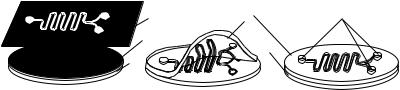
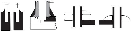
The gripper was designed for the normally closed operation mode. That means the gripper is not actuated while holding an object. Actuation is only needed during the gripping and release actions. This design minimizes the thermal load on the object. Figure 5.6g shows the design and the corresponding geometry parameters of the polymeric microgripper. The gripper is suspended on a frame that supports the fragile structures during the release and assembly process and is removed before use. The gripper consists of two symmetrical arms. The tip has a gap of 30 µm. The L-shaped slit on the tip limits further the gripping force allowing gentle handling of the object. Each gripper arm consists of three flexures. Two small flexures with a width of 100 µm act as the “hot” arms of the thermal actuator. The large flexure works as the “cold” arm of the actuator. Holes with an 100-µm diameter are incorporated in the large flexure to allow easy etch access for the later release. The circular holes and the rounded corner arrest the possible stress in SU-8 during the fabrication and avoid cracks in the gripper. With this design the gripper is attached to the base with 6 flexures, which warrant mechanical stability for the relatively long gripper arms. Figure 5.7a shows the fabricated gripper.
Figure 5.7b depicts the measured displacement/voltage characteristics of the gripper. The circles are the measured data. The solid line is the second order polynomial fitting function. The typical quadratic behavior can be observed.
5.3.3. Replication Technologies
Replication technologies allow the mass fabrication of BMMDs at a low cost. Since most of the BMMDs have a relatively large size compared to conventional MEMS-devices
|
110 |
|
|
|
|
|
|
100 |
|
|
|
|
|
|
90 |
|
|
|
|
|
( m) |
80 |
|
|
|
|
|
70 |
|
|
|
|
|
|
Displacement |
|
|
|
|
|
|
40 |
|
|
|
|
|
|
|
60 |
|
|
|
|
|
|
50 |
|
|
|
|
|
|
30 |
|
|
|
|
|
|
20 |
|
|
|
|
|
(a) |
10 |
|
|
|
|
|
|
|
|
|
|
|
|
|
0 |
|
|
|
|
|
|
0 |
2 |
4 |
6 |
8 |
10 |
Voltage (V)
(b)
FIGURE 5.7. The fabricated microgripper (a) and its characteristics (b).
FABRICATION ISSUES OF BIOMEDICAL MICRO DEVICES |
105 |
and consequently the small number of devices on a wafer. Thus, silicon technologies could be very expensive for BMMDs.
The basic idea behind replication technologies is the fabrication of a master mold with the “expensive” technology and the low-cost replication in polymers. However, the major drawbacks of replication technologies are [1]:
–Since the master is to be removed from the molded structures, free standing structures with undercuts can not be fabricated. A combination with polymeric surface micromachining (section 5.3.2) could be a solution for this problem.
–Only few micromachining technologies can meet the required smoothness of the master mold.
–Due to contamination and fast diffusion in micro scale, release agents used in macro scale can not be used for the release process in microscale.
The master mold can be fabricated with a number of techniques. Conventional machining techniques such as drilling, cutting, milling, and turning can be used for this purpose for structures down to several tens microns. Bulk silicon micromachining can be used for structures with high aspect-ratios. Metal mold can be electro platted with the help of a structured thick resists such as SU-8 and PMMA. For instance, the fabrication of nickel mold from structured PMMA was established and called as LIGA (Lithographie, Galvanoformung, Abformung) (German acronym for lithography, electroplatting, and molding). Following, three replication techniques are discussed in details: soft lithography, hot embossing, and injection molding.
5.3.3.1. Soft Lithography Soft lithography is a direct pattern transfer technique. The technique is based on an elastomeric stamp with patterned relief structures on its surface. There are two basic techniques for transferring the micro patterns: micro contact printing and replica molding [38]. In many BMMDs, the elastomeric part can be used directly as the functional material. Following the fabrication of microchannels with PDMS are described.
To start with, PDMS is mixed from prepolymers. The weight ratio of the base and the curing agent could be 10:1 or 5:1. The solid master is fabricated from SU-8, Fig. 5.8a. Glass posts can be placed on the SU-8 master to define the inlets and reservoirs.
Next, the PDMS mixture is poured into the master and stands for a few minutes in order to self-level, Fig. 5.8b. The whole set is then cured at relatively low temperature from 60 ◦C to 80 ◦C for several hours. After peeling off and having surface treatment with
Mask |
PDMS |
Access holes |
SU8 |
Glass |
|
|
|
|
Si |
|
|
(a) |
(b) |
(c) |
FIGURE 5.8. Fabrication of micro channels with soft lithography: (a) fabrication of a SU-8 master, (b) making a PDMS replica, (c) surface treatment in oxygen plasma and bonding to glass.
106 |
NAM-TRUNG NGUYEN |
low-temperature oxygen plasma. The structured PDMS membrane is brought into contact with clean glass, silica, or another piece of surface-activated PDMS, Fig. 5.8c.
The sealed channel can withstand pressures up to five bars. Without surface treatment, PDMS also forms a watertight seal when pressed against itself, glass, or most other smooth surfaces. These reversible seals are useful for detachable fluidic devices, which are often required in research and prototyping. Inlet tubes and outlet tubes can be embedded in the PDMS device [16].
Three-dimensional structures can be formed by lamination of many PDMS sheets. In this case. methanol is used as surfactant for both bonding and self-alignment. The surface tension at superimposed holes in the PDMS sheets self-aligns them. Methanol prevents instant bonding between two PDMS sheets after plasma treatment. After evaporating methanol on a hot plate, the laminated stack is bonded.
5.3.3.2.Hot Embossing Hot embossing was widely used for the fabrication of simple microchannels. The technique uses a master mold and a flat polymer substrate. The polymer
substrate is heated above the glass transition temperatures, which are typically on the order of 50 ◦C to 150 ◦C. Embossing force (0.5 to 2 kN/cm2) is then applied on the substrate under vacuum conditions [1]. Before release, the master and the substrate are cooled under the applied embossing force. The entire hot-embossing process takes about few minutes.
5.3.3.3.Injection Molding Injection molding is a standard process for fabricating polymer parts. Using a micromachined mold insert, this technique can be extended to the fabrication of BMMDs. Injection molding uses polymer in granular form. The polymer is first transported into a cylinder with a heated screw, where the granules are melted. The
melt is forced into the mold insert with a high pressure (600 to 1000 bars). The molding temperature depends on the type of the polymer (about 200 ◦C for PMMA and PS, about 280 ◦C for PC) [1]. For micro devices, the mold isert needs to be heated close to the glass transition temperature of the polymer. The entire injection molding process takes about 1 to 3 minutes.
5.3.4.Laser Machining
Laser machining is a localized, non-contact machining technique. Machining applications of laser include drilling, cutting, engraving, marking and texturing. Almost all types of material such as metals, ceramics, plastics, and wood can be used with laser machining. Most significantly, laser machining can remove materials in small amount with a small heat-affected zone. Micromachining with controlled accuracy can be achieved. A further attractive advantage of laser machining compared to other micromachining techniques is the possibility of low-cost rapid prototyping.
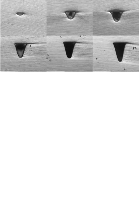
UV-lasers were used to realize microstructures in polymers. For more detailed discussion on the mechanism on UV-laser ablation on PMMA the reader can refer to [33]. Although UV-laser is a good choice for laser ablation, its cost is much higher than that of CO2-laser. CO2-laser has a relatively long characteristic wavelength of 10.6 µm. Thus, the ablation process depends more on thermal energy. The microchannels shown in Fig. 5.9 were fabricated by the Universal M-300 Laser Platform of Universal Laser Systems Inc. (http://www.ulsinc.com). The system uses a 25-Watt CO2-laser, the maximum beam moving
FABRICATION ISSUES OF BIOMEDICAL MICRO DEVICES |
107 |
FIGURE 5.9. Typical shapes of microchannels fabricated with CO2-laser in PMMA.
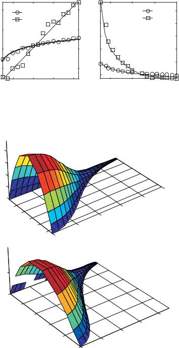
speed is about 640 mm/s. When the laser beam driven by stepper motors moves across the substrate surface, it engraves a microchannel into the substrate. As mentioned above, the ablation process of CO2-laser is determined by thermal energy. Therefore the cross section of the microchannel depends on the energy distribution of the laser beam, its moving speed, the laser power, and the thermal diffusivity of substrate material. The energy of the laser beam has a Gaussian distribution, thus the cross section of the channel also has a Gaussian shape. Typical cross sections of Gaussian-shaped microchannels can be seen in Fig. 5.9. Klank et al. [17] found a linear relation between the channel depth and the laser power as well as the number of scanning passes. Beside these two parameters, the influence of the beam speed on the cross-section geometry is shown in Fig. 5.10b.
For the results in Fig. 5.10a the beam speed is fixed at 4%, while the laser power is varied from 3% to 10.5%. The channel depths increase linearly with the laser power as observed by [17]. However the relation between the channel width and the laser power is not linear. For the results in Fig. 5.10b the laser power was kept at a constant value of 7%, while the beam speed is varied from 1.1% to 8%. We can observe that the channel widths and channel depths are inversely proportional to the beam speed.
Figure 5.11 shows the typical velocity distribution in a Gaussian-shaped microchannel. The Poiseuille number Po represents the fluidic resistance of a microchannel and is defined as:
|
1 d p D2 |
|
|
Po = − |
h |
, |
(5.1) |
µ dx 2u |
where µ is the viscosity of a fluid, d p/dx is the pressure gradient along the channel, Dh is the hydraulic diameter, and u is the average velocity. The Poiseuille number only depends on the channel shape. Gaussian-shaped channels have a Poiseuille number ranging from 9 to 15 depending on the aspect ratio α = H/ W between the depth H and the width W ,
Consant beam speed of 4% |
Constant laser power of 7% |
Geometry parameters ( m)
400
300
200
100
|
Width |
|
( m) |
1200 |
|
|
Width |
|
|
Depth |
|
|
|
|
Depth |
|
|
|
|
|
parameters |
1000 |
|
|
|
|
|
|
|
|
|
|
|
|
|
|
|
|
|
800 |
|
|
|
|
|
|
|
Geometry |
600 |
|
|
|
|
|
|
|
400 |
|
|
|
|
|
|
|
|
|
|
|
|
|
|
|
|
|
|
200 |
|
|
|
|
4 |
6 |
8 |
10 |
|
2 |
4 |
6 |
8 |
|
Relative power (%) |
|
|
|
Relative beam speed (%) |
|
||
|
(a) |
|
|
|
|
(b) |
|
|
FIGURE 5.10. Geometry parameters of the microchannels as functions of laser power and laser speed. The relative values are based on a maximum laser power of 25 W and a maximum beam speed of 640 mm/s. Circles and squares are measurement results, lines are fitting curves.
2 |
|
|
|
1.5 |
|
|
|
u* |
|
|
|
1 |
|
|
|
0.5 |
|
|
|
0 |
|
|
0.5 |
|
|
0.4 |
|
|
|
|
|
-0.05 |
|
|
0.3 |
-0.1 |
|
0.2 |
x* |
-0.15 |
|
||
|
|
||
y* |
-0.2 |
0.1 |
|
|
-0.25 |
|
|
0(a)
2 
1.5 
u* 1
0.5 


0 
0
-0.1
-0.2 |
|
0.4 |
|
y* |
-0.3 |
0.3 |
|
x* |
|||
|
0.2 |
-0.4
0.1
-0.5 0
(b)
FIGURE 5.11. Simulated velocity distribution of a pressure driven flow Gaussian-shaped microchannels:
(a) Aspect ratio of α = 0.25, (b) Aspect ratio of α = 0.5.
FABRICATION ISSUES OF BIOMEDICAL MICRO DEVICES |
109 |
while circular channels and slit channels have higher Poiseuille numbers Po = 16 and Po = 24, respectively.
5.4. PACKAGING OF BIOMEDICAL MICRO DEVICES
The challenges in packaging of BMMDs are the many types of interconnects on the same micro device. In addition to electric interconnects, fluidic interconnects are also needed. The packaging technology should assure the interfaces between the electric domain, fluidic domain and the external environment. Three basic packaging concepts for BMMDs are the multi-chip module, the monolithic horizontal integration and the stacked modular system [18].
–Multi-chip module (MCM) concept is similar to the concept of a printed circuit board (PCB). The MCM concept bonds unpackaged chips to a carrier substrate, which has both electrical wires and fluidic channels. The assembly technique for this concept can be adapted from the surface-mounted technology of traditional electronics.
–Stacked modular system is based on the modular concept of MCM. The components can be stacked as modules to form a complex system.
–Monolithic horizontal integration realizes all components in the same substrate in the same fabrication process. This concept is similar to the monolithic integration of microelectronic components. The advantage of this abroach are the small total size, minimum dead volume and leak-free fluidic interconnects. The drawback is the complex process involved and the many masks needed. Most of the BMMDs have device-specific fabrication processes, which may not be compatible to the rest of the fabrication.
Following, some typical packaging techniques related to polymeric BMMDs are discussed in details.
5.4.1. Thermal Direct Bonding
Similar to diffusion bonding, the direct bonding of the polymeric parts is based on thermal reaction. The strength of most thermoplastics will change with temperature. With the temperature increase the molecules have higher kinetic energy, which breaks the bondage between the monomers. The damage of the molecular chains in a polymer depends on the extent of the absorbed energy.
There are two significant temperature points in the thermal behavior of most thermoplastics: the glass transition temperature and the start of the random chain scission phase. At the glass transition point, the plastics will lost the strength at the normal temperature, but still can keep it solid shape. In the random chain scission phase the bondage between the monomers will be damaged rapidly, and the plastics will lost its solid shape. In a thermal bonding process, this phase will damage some old bondage and form new bondage between the polymer substrates.
The bonding temperature can be selected just above glass transition temperature (106 ◦C for PMMA), so the substrates and the structures on the surface can keep their original shapes. However, bonding at glass transition temperature has the problem of low bonding energy, thus the bondage between surfaces is not very strong. Bonding at a higher temperature will
110 |
NAM-TRUNG NGUYEN |
cause the polymer structures to lost its original shapes. Fortunately, the thermal degradation of a polymer starts much later than the glass transition temperature (150 ◦C for PMMA), and the weak head group of monomers will be damaged at a higher temperature (near 180 ◦C for PMMA). From this temperature on the speed of the degradation of the polymer is very fast and it will lose its original shapes. A temperature slightly above the thermal degradation point could be chosen for thermal bonding of polymers. For instance, a temperature of 165 ◦C is a good bonding temperature for PMMA. At this temperature a good balance between keeping shape and high bond strength can be achieved. Following the bonding process of two PMMA-wafers is described.
To start with, the PMMA wafers are cleaned with IPA and rinsed in DI-water in an ultrasonic bath. The actual bonding process can be carried out in a commercial wafer bonder for silicon wafers. The process is similar to fusion bonding between silicon wafers. First, the wafers were heated up to 165 ◦C. This temperature remains for the next 30 minutes. Fast cooling may cause residual stress in the wafer stack. Thus an anneal process should be carried out after the high temperature process. The anneal temperature for PMMA is about 80 ◦C.
To avoid bubbles at the bond interface, a pressure of about 1 bar is to be applied on the wafer stack. Another measure can improve the bonding quality is to design channels on the chips to trap and vent out the gas.
5.4.2. Adhesive Bonding
Adhesive bonding uses an intermediate layer to bond 2 wafers. The advantages of adhesive bonding are the low process temperature and the ability to bond different polymeric materials. The intermediate layer can be an adhesive, which can be cured with temperature or UV-exposure. The example in section 5.3.1.2 used a thin SU-8 layer as the adhesive.
Liquid adhesive may block microchannels and other micro components. An alternative to coating an adhesive layer is the use of a pre-fabricated double-sided adhesive. In the example of a stand-alone micropump in section 5.3.2.1, a 50-µm-thick adhesive tape (Arclad 8102, Adhesive Research Inc., Clen Rock, PA) were used as the intermediate bonding layer. The lamination of the adhesive layers allows bonding at room temperature, which is of advantage for fully polymeric devices with different material layers.
5.4.3. Interconnects
One of the biggest challenge in the fabrication of BMMDs is the development of low-cost fluidic interconnects to the macroscopic world. A BMMD in general needs interconnects for power supply, information signals, and material flow to communicate with its environment. The material flow is the fluid flow, which is processed in a BMMD. While traditional microelectronics already offers a number of solutions for the first two types of interconnects, fluidic interconnects still pose a big challenge to the design and fabrication of BMMDs. Fluidic interconnects for BMMDs should meet some general requirements:
–Easy to handle,
–Low dead volume,
–High-pressure resistance,
–Small sizes,
–Chemical and biological compatibility.
FABRICATION ISSUES OF BIOMEDICAL MICRO DEVICES |
111 |
In the following sections, fluidic interconnects are categorized by the coupling nature as press-fit interconnects and glued interconnects.
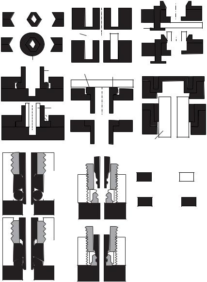
5.4.3.1.Press-Fit Interconnects Press-fit interconnects utilize elastic forces of coupling parts to seal the fluidic access. Due to the relatively small sealing forces, this type of interconnect is only suitable for low-pressure applications. For fluidic coupling out of a BMMD, tubing interconnects are needed. Figure 5.12a shows a horizontal tubing interconnect fabricated by wet etching of silicon. The external polymeric tubing is press-fitted to the silicon tubing [8]. Vertical tubing interconnects can be etched in silicon using DRIE, Fig. 5.12b. These vertical tubes can hold fused silica capillaries, which are perpendicular to the device surface. If external capillaries are to be inserted directly into etched openings, plastic couplers can be used to keep them, Fig. 5.12c [8].
The molded coupler shown in Figure 5.12d is fabricated from two bonded silicon wafers. The fused silica capillary is embedded in the plastic coupler. The capillary with the coupler is then inserted into the fluidic opening. Annealing the device at elevated temperatures allows the plastic to melt. After cooling down to room temperature, the plastic coupler seals the capillary and the opening hermetically [25]. Plastic couplers can also be compression-molded. The thermoplastic tube is inserted into the opening. Under pressure and temperatures above the glass transition temperature, the plastic melts and fills the gaps between the coupler and silicon, Fig. 5.12e.
In many cases, the elastic force of the couplers can not withstand high pressures. One solution for high pressure interconnects is the use of a mesoscale casing, which has conventional O-rings for sealing fluidic interconnects. If a microfluidic system has multiple fluidic ports, many small O-rings are required. In this case, it is more convenient to have integrated O-rings in the device [39]. First, the cavities for the O-rings are etched in silicon with DRIE. After depositing an oxide/nitride layer, silicone rubber is squeezed into the cavities . The fluidic access is opened from the backside by DRIE. Subsequently, the oxide/nitride layer is etched in buffered hydrofluoric acid and SF6 plasma. The silicone rubber O-ring remains on top of the opening. If a capillary is inserted into the opening, the rubber O-ring seals it tightly, Fig. 5.12f.
Figure 5.12g shows a concept with standard polyetheretherketone (PEEK) tubing for high performance liquid chromatography (HPLC) [18]. The PEEK tubing is machined to fit the ferrule and the O-ring as shown in Fig. 5.12g. The tube is inserted through the hollow screw. Tightening the screw presses the O-ring against the fluidic port of the BMMD. The O-ring can be replaced by a custom molded ring as shown in Fig. 5.12g [18].
5.4.3.2.Glued Interconnects In many cases, press-fit interconnects are fixed with adhesives. Besides holding function, adhesives offer good sealing by filling the gap between the external tubes and the device opening. Figure 5.13a shows a typical glued fluidic interconnects. The glued surface can be roughened to improve adhesion. A combination of surface roughening, compression molding, and adhesive bonding is used to make tight fluidic interconnects, Fig. 5.13b [36].
If epoxy is to be avoided, metal alloy such as Kovar can be used as the sealing material. Kovar is an alloy consisting of 29% nickel, 17% coper, and the balance of iron. Because of its relatively low thermal expansion coefficient, Kovar is often used for glass to metal
112
|
Glass capillary |
(a) |
(b) |
|
Polymeric tubing |
|
Polymeric coupler |
Glass capillary
(d) |
(e) |
(g) |
(h) |
NAM-TRUNG NGUYEN
(c)
(f)Glass tubing
Silicon Glass
SiO2 /Si3N4 Polymers
FIGURE 5.12. Examples of press-fit interconnects.
seals in electronics packaging. Figure 5.13d shows a solution with glass seal and Kovar tubes [20]. The Kovar tubes are fitted into the fluidic access. Glass beads are placed around them. A carbon fixture is used as the mold for the glass melt. Glass sealing is accomplished after annealing the assembly at 1,020 ◦C [20].
FABRICATION ISSUES OF BIOMEDICAL MICRO DEVICES |
113 |
|
Glass tubing |
Polymer tubing |
|
|
|
Kovar tubing |
|
|
|
|
|
|
|
|
|
|
|
|
|
|
(d) |
|
|
|
|
|
|
|
|
|
|
|
|
|
|
|
|
|
|
|
|
|
|
|
|
|
|
|
|
|
|
|
|
|
|
|
|
|
|
|
|
|
|
|
|
|
|
|
|
(a) |
|
|
|
|
(b) |
|
|
|
|
|
|
|
|
|
|
|
|
|
|
|
|
|
|
|
|
|
|
|
|
|
|
|
|
|
|
|
|
|
|
||
|
|
|
|
|
Metal |
|
|
|
|
Silicon |
|
|
Glass |
|
|
Polymer |
||||
|
|
|
|
|
|
|
|
|
|
|
|
|
|
|
|
|
|
|
|
|
|
|
|
|
|
|
|
|
|
|
|
|
|
|
|
|
|
|
|
|
|
|
|
|
|
|
|
|
|
|
|
|
|
|
|
|
|
|
|
|
|
|
FIGURE 5.13. Examples of press-fit interconnects.
5.5. BIOCOMPATIBILITY OF MATERIALS AND PROCESSES
5.5.1. Material Response
The most common material responses to the biological environment are swelling and leaching. The simplest material response is a mass transfer across the tissue/material interface. Fluid diffuses from the host tissue into the device material, causing it to swell. The changes in dimension may cause microcracks on the material’s surface, which in turn alter the mechanical properties of the device. Leaching is another reaction caused by fluid transfer. The fluid that had previously diffused into the device material can move back into the biological environment, and carries material particulates suspended within. Removed particulates damage both the device and surrounding tissues.
5.5.2. Tissue and Cellular Response
Reactionary tissue response begins with inflammation at the device/tissue interface. The symptoms of inflammation are classically reddening, swelling, heating, and pain. Chemical signals released by the damaged tissue trigger the inflammation and attract white blood cells as body response. The device is covered with macrophages and foreign body giant cells leading to a fibrous encapsulation. The encapsulation can affect the functionality of the device [40].
If the healing process occurs as described above, the device can be called biocompatible. Alternatively, a long-lasting inflammation can be caused by chemical or physical properties of the device material or by motion of the device itself. Constant local cell damages make an inflammation reaction continue to be released. If the device material causes cells to die, it is called cytotoxic. If the device material is inert, its particulates cannot be digested by macrophages. The material response to the biological environment can cause chemical changes in the device material, which can be cytotoxic and damage cells.
5.5.3. Biocompatibility Tests
There are two general test methods for biocompatibility:
–In vitro (in laboratory glassware);
–In vivo (in a live animal or human).