

Biomolecular Sensing Processing and Analysis - Rashid Bashir and Steve Wereley
.pdfIMPLANTABLE WIRELESS MICROSYSTEMS |
207 |
with packaging and reliability has prevented their successful application. MEMS-based microsensors have been more successful and offer several advantages compared to the macrodomain counterparts. These include lower power consumption, increased sensitivity, higher reliability, and lower cost due to batch fabrication. However, they suffer from a poor signal to noise ratio hence requiring a close by interface circuit. Among the many microsensors designed and fabricated over the past two decades, physical sensors have been by and large more successful. This is due to their inherent robustness and isolation from any direct contact with biological tissue in sensors such as accelerometers and gyroscopes. Issues related to packaging and long-term stability have plagued the implantable chemical sensors. Long-term baseline and sensitivity stability are major problems associated with implantable sensors. Depending on the type of the sensor several different factors contribute to the drift. For example in implantable pressure sensors, packaging generated stresses due to thermal mismatch and long-term material creep are the main sources of baseline drift. In chemical sensors, biofouling and fibrous capsule formation is the main culprit. Some of these can be mitigated through clever mechanical design and appropriate choice of material, however, some are more difficult to prevent (e.g., biofouling and fibrous capsule formation). Recent developments in the area of anti-fouling material and controlled release have provided new opportunities to solve some of these long standing problems [15–17].
10.2.2. Interface Electronics
As was mentioned previously, most MEMS-based transducers suffer from poor signal to noise ratio and require on-board interface electronics. This of course is also more so essential for implantable microsystems. The choice of integrating the signal processing with the MEMS transducer on the same substrate or having a separate signal processing chip in close proximity depends on many factors such as process complexity, yield, fabrication costs, packaging, and general design philosophy. Except post-CMOS MEMS processing methods, which rely on undercutting micromechanical structures subsequent to the fabrication of the circuitry [18], other integrated approaches require extensive modifications to the standard CMOS processes and have not been able to attract much attention. Post-CMOS processing is an attractive approach although packaging issues still can pose roadblocks to successful implementation. Hybrid approach has been typically more popular with the implantable microsystem designers providing flexibility at a lower cost. Power consumption is a major design consideration in implantable wireless microsystems that rely on batteries for an energy source. Low-power and sub-threshold CMOS design can reduce the power consumption to nW levels [19–23]. Important analog and mixed-signal building blocks for implantable wireless microsystems include amplifiers, oscillators, multiplexers, A/D and D/A converters, and voltage references. In addition many such systems require some digital signal processing and logic function in the form of finite-state machines. In order to reduce the power consumption, it is preferable to perform the DSP functions outside the body although small finite-state machines can be implemented at low power consumptions.
10.2.3. Wireless Communication
Bi or uni-directional wireless communication is a central feature in all implantable wireless microsystems. In systems that are powered from outside using inductive link
208 |
BABAK ZIAIE |
bi-directional communication can be achieved using several techniques [24]. The inward link can be easily implemented using amplitude modulation, i.e., the incoming RF signal that powers the microsystem is modulated by digitally varying the amplitude. It is evident that the modulation index can not be 100% since that would cut off the power supply to the device (unless a storage capacitor is used). The coding scheme is based on the pulse time duration, i.e., “1” and “0” have the same amplitude but different durations [5, 25]. This modulation technique requires a simple detection circuitry (envelope detector) and is immune to amplitude variations, which are inevitable in such systems. The outward link can be implemented using two different techniques. One relies on “load modulation”, i.e., the outgoing digital stream of data is used to load the receiver antenna [26]. This can be picked up through the transmitter coil located outside the body. The second technique is more complex and requires an on-chip transmitter and a second coil to transmit the recorded data at a different frequency.
Battery operated implantable wireless microsystems rely on different communication schemes. Outward data transmission can be accomplished using any of the several modulation schemes (AM, FM, and other pulse modulation methods) which offer standard trade offs between transmitter and receiver circuit complexity, power consumption, and signal to noise ratio [27]. Inward transmission of data can also be accomplished in a similar fashion. Typical frequencies used in such systems are in the lower UHF range (100–500 MHz). Higher frequencies result in smaller transmitter antenna at the expense of increased tissue loss. Although tissue loss is a major concern in transmitting power to implantable microsystems; it is less of an issue in data transmission since a sensitive receiver outside the body can easily demodulate the signal. Recent explosive proliferation of wireless communication systems (cell phones, wireless PDAs, Wi-Fi systems, etc.) have provided a unique opportunity to piggy back major RFIC manufacturers and simplify the design of implantable microdevices [28–30]. This can not only increase the performance of the system but also creates a standard platform for many diverse applications. Although the commercially available wireless chips have large bandwidths and some superb functionality, their power consumption is higher than what is acceptable for many of the implantable microsystems. This however, is going to be changed in the future by the aggressive move towards lower power handheld consumer electronics.
10.2.4. Power Source
The choice of power source for implantable wireless microsystems depends on several factors such as implant lifetime, system power consumption, temporal mode of operation (continuous or intermittent), and size. Progress in battery technology is incremental and usually several generations behind other electronic components [31]. Although lithium batteries have been used in pacemakers for several years, they are usually large for microsystem applications. Other batteries used in hearing aids and calculators are smaller but have limited capacity and can only be used for low power systems requiring limited lifespan or intermittent operation. Inductive powering is an attractive alternative for systems with large power requirements (e.g., neuromuscular stimulators) or long lifetime (e.g., prosthetic systems with >5 years lifetime) [7]. In such systems a transmitter coil is used to power a microchip using magnetic coupling. The choice of the transmission frequency is a trade off between adequate miniaturization and tissue loss. For implantable microsystems the frequency range of 1–10 MHz is usually considered optimum for providing adequate
IMPLANTABLE WIRELESS MICROSYSTEMS |
209 |
miniaturization while still staying below the high tissue absorption region (>10 MHz) [32]. Although the link analysis and optimization methods have been around for many years [33], recent integration techniques that allow the fabrication of microcoils on top of CMOS receiver chip has allowed a new level of miniaturization [34]. For applications that require the patient carry the transmitter around, a high efficiency transmitter is required in order to increase the battery lifetime. This is particularly critical in implantable microsystem, where the magnetic coupling between the transmitter and the receiver is low (<1%). Class- E power amplifier/transmitters are popular among microsystem designers due to their high efficiency (>80%) and relatively easy design and construction [5, 35, 36]. They can also be easily amplitude modulated through supply switching.
Although ideally one would like to be able to tap into the chemical reservoir (i.e., glucose) available in the body to generate enough power for implantable microsystems (glucose based fuel cell), difficulty in packaging and low efficiencies associated with such fuel cells have prevented their practical application [37]. Thin-film batteries are also attractive, however, there still remain numerous material and integration difficulties that need to be resolved [38]. Another alternative is nuclear batteries. Although they have been around for several decades and were used in some early pacemakers, safety and regulatory concerns forced medical device companies to abandon their efforts in this area. There has been a recent surge of interest in microsystem nuclear batteries for military applications [39]. It is not hard to envision that due to the continuous decrease in chip power consumption and improve in batch scale MEMS packaging technology, one might be able to hermetically seal a small amount of radioactive source in order to power an implantable microsystem for a long period of time. Another possible power source is the mechanical movements associated with various organs. Several proposals dealing with parasitic power generation through tapping into this energy source have been suggested in the past few years [40]. Although one can generate adequate power from activities such as walking to power an external electronic device, difficulty in efficient mechanical coupling to internal organ movements make an implantable device hard to design and utilize.
10.2.5. Packaging and Encapsulation
Proper packaging and encapsulation of implantable wireless microsystems is a challenging design aspect of such microdevices. The package must accomplish two tasks simultaneously: 1) protect the electronics from the harsh body environment while providing access windows for transducers to interact with the desired measurand, and 2) protect the body from possible hazardous material in the microsystem. The second task is easier to fulfill since there is a cornucopia of various biocompatible materials available to the implant designer [41]. For example, silicon and glass, which are the material of choice in many MEMS applications, are both biocompatible. In addition, polydimethylsiloxane (PDMS) and several other polymers (e.g., polyimide, polycarbonate, parylene, etc.) commonly used in microsystem design are also accepted by the body. The first requirement is however more challenging. The degree of protection required for implantable microsystems depends on the required lifetime of the device. For short durations (several months) polymeric encapsulants might be adequate if one can conformally deposit them over the substrates (e.g., plasma deposited parylene) [42]. These techniques are considered non-hermetic and have limited lifetime. For long term operation, hermetic sealing techniques are required [43]. Although pacemaker and defibrillator industries have been very successful in sealing their
210 |
BABAK ZIAIE |
systems in tight titanium enclosures; these techniques are not suitable for microsystem applications. For example a metallic enclosure prevents the transmission of power and data to the microsystem. In addition, these sealing methods are serial in nature (e.g., laser or electron beam welding) and not compatible with integrated batch fabrication methods used in microsystem design. Silicon-glass electrostatic and silicon-silicon fusion bonding are attractive methods for packaging implantable microsystems [44]. Both of these bonding methods are hermetic and can be performed at the wafer level. These are particularly attractive for inductively powered wireless microsystems since most batteries can not tolerate the high temperatures required in such substrate bondings. Other methods such as metal electroplating have also been used to seal integrated MEMS microsystems. However, their long term performance is usually inferior to the anodic and fusion bondings. In addition to providing a hermetic seal, the package must allow feeedthrough for transducers located outside the package [45]. In macrodevices such as pacemakers where the feedthrough lines are large and not too many, traditional methods such as glass-metal or ceramic-metal has been employed for many years. In microsystems such methods are not applicable and batch scale techniques must be adopted.
10.3. DIAGNOSTIC MICROSYSTEMS
Diagnostic wireless microsystems are used to gather physiological or histological information from within the body in order to identify pathology. In this category, we will discuss two recent examples. The first one is a microsystem designed to be implanted in the eye and measure the intraocular pressure in order to diagnose low-tension glaucoma. The second system although not strictly implanted is an endoscopic wireless camera-pill designed to be swallowed in order to capture images from the digestive track.
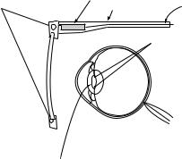
Figure 10.1 shows the schematic diagram of the intraocular pressure (IOP) measurement microsystem [46, 47]. This device is used to monitor the IOP in patients suffering from
|
external telemetric |
|
|
external coil |
components |
|
|
spectacles |
cable to hand-held-unit |
||
|
pressure sensor,
internal telemetric components
 eye
eye
artificial intraocular lens
FIGURE 10.1. Schematic of the IOP measurement microsystem [46].
IMPLANTABLE WIRELESS MICROSYSTEMS |
211 |
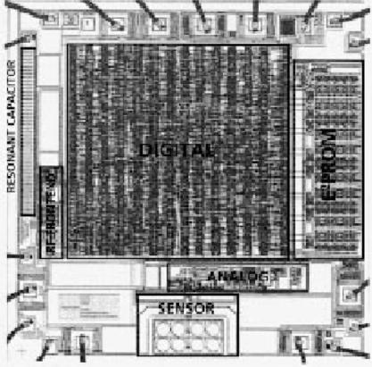
FIGURE 10.2. Micrograph of the IOP measurement microsystem receiver chip showing surface micromachined capacitive pressure sensors and other parts of the receiver circuitry [47].
low tension glaucoma, i.e., the pressure measured in the doctor’s office is not elevated (normal IOP is 10–20 mmHg) while the patient is showing optics nerve degeneration associated with glaucoma. There is a great interest in measuring the IOP in such patients during their normal course of daily activity (exercising, sleeping, etc). This can only be achieved using a wireless microsystem. The system shown in Figure 10.1 consists of an external transmitter mounted on a spectacle, which is used to power a microchip implanted in the eye. A surface micromachined capacitive pressure sensor integrated with CMOS interface circuit is connected to the receiving antenna. The receiver chip implemented in an n-well 1.2 µm CMOS technology has overall dimensions of 2.5 × 2.5 mm2 and consumes 210 µW, Figure 10.2. The receiver polyimide-based antenna is however much larger (1 cm in diameter and connected to the receiver using flip chip bonding) requiring the device to be implanted along with an artificial lens. The incoming signal frequency is 6.78 MHz while the IOP is transmitted at 13.56 MHz using load-modulation scheme. This example illustrates the levels of integration that can be achieved using low power CMOS technology, surface micromachining, and flip chip bonding.
212 |
BABAK ZIAIE |
Antenna |
CMOS image |
|
Lens |
Optical dome
ASIC |
Batteries |
White LED |
transmitter |
|
|
|
|
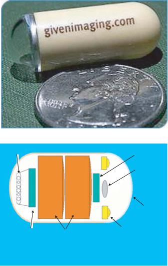
Wireless Capsule Endoscope
FIGURE 10.3. A photograph (top) and internal block diagram (bottom) of Given Imaging wireless endoscopic pill. (Courtesy Given Imaging)
The second example in the category of diagnostic microsystems is an endoscopic wireless pill shown in Figure 10.3 [48–50]. This pill is used to image small intestine, which is a particularly hard area to reach using current fiber optic technology. Although these days colonoscopy and gastroscopy are routinely performed, they can not reach the small intestine and many disorders (e.g., frequent bleeding) in this organ have eluded direct examination. A wireless endoscopic pill can not only image the small intestine, but also will reduce the pain and discomfort associated with regular gastrointestinal endoscopies. The endoscopic pill is a good example of capabilities offered by advanced consumer microelectronics. Although
IMPLANTABLE WIRELESS MICROSYSTEMS |
|
213 |
||||||||||||
Focusing |
|
Tank A for |
Capacitor |
|||||||||||
Magnetic coil |
tissue sampling |
|||||||||||||
|
|
|
|
|
|
|
|
|
|
|
||||
Near-infrared |
Valve |
|
Direction control rotor coil |
|||||||||||
|
|
|
||||||||||||
LED |
|
|
|
(A, B, C) |
||||||||||
White LED |
|
|
|
|
Micro wave video |
|||||||||
|
|
|
|
|
||||||||||
|
|
|
|
|
signal transmitter |
|||||||||
|
|
|
|
Electric power |
||||||||||
Optical dome |
|
|
|
generating magnetic coil |
||||||||||
|
|
|
|
|
|
|
|
|
|
|
|
|
||
|
|
|
Tank B for |
|
|
|
|
|
[Dimensions] |
|||||
Tube |
|
|
|
|
|
|
|
|
|
|
|
|
||
|
Valve |
spray medication |
|
|
|
|
|
|
|
|||||
|
|
|
|
|
|
|
|
|||||||
LED with alternative wavelength |
|
f |
9mm |
|
|
|
|
|
|
|
||||
|
|
|
|
|
|
|
|
|||||||
|
|
|
|
|
|
|
|
|
|
|
||||
|
|
|
|
|
|
|
|
|
|
|
||||
|
|
|
|
|
|
|
|
|
|
|
|
|
|
|
|
|
|
|
|
|
|
|
|
|
23mm |
|
|
|
|
|
|
|
|
|
|
|
|
|
|
|
||||
|
|
|
|
|
|
|
|
|
|
|
|
|
|
|
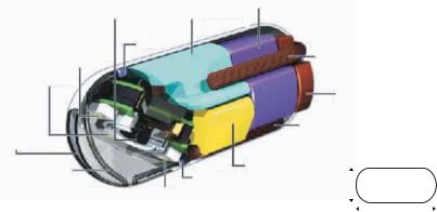
FIGURE 10.4. A schematic of the RF Systems wireless video pill. (Courtesy RF Systems Lab)
the idea of a video pill is not new, before the development of low-power microelectronics, white LED, CMOS image sensor, and wide band wireless communication, fabrication of such a device was not feasible. The video pill currently marketed by Given Imaging is 11 mm in diameter and 30 mm in length (size of a large vitamin tablet) and incorporates: 1) a short focal length lens, 2) a CMOS image sensor (90,000 pixel), 3) four white LEDs, 4) a low power ASIC transmitter, and 5) two batteries (enough to allows the pill to go though the entire digestive track). The pill can capture and transmit 2 images/second to an outside receiver capable of storing up to 5 hours of data. Another company (RF Systems Lab.) is also developing a similar microsystem using a higher resolution CCD (410,000 pixel) camera (30 images/second) and inductive powering, Figure 10.4 [51].
10.4. THERAPEUTIC MICROSYSTEMS
Therapeutic microsystems are designed to alleviate certain symptoms and help in the treatment of a disease. In this category, we will describe two such microsystems. The first one is a drug delivery microchip designed to administer small quantities of potent drugs upon receiving a command signal from the outside. The second device is a passive micromachined glucose transponder, which can be used to remotely monitor glucose fluctuations allowing a tighter blood glucose control through frequent measurements and on-demand insulin delivery (pump therapy or multiple injections)
Figure 10.5 shows the central component of the drug delivery microchip [52, 53]. It consists of several micro-reservoirs (25 nl in volume) etched in a silicon substrate. Each
˚
micro-reservoir contains the targeted drug and is covered by a thin gold membrane (3000 A), which can be dissolved through the application of a small voltage (1 V vs. SCE), Figure 10.5. The company marketing this technology (MicroCHIPS Inc.) is in the process of designing a wireless transceiver that can be used to address individual wells and release the drug upon the reception of the appropriate signal [54]. Another company (ChipRx Inc.) is also aiming to develop a similar microsystem (Smart Pill), Figure 10.6 [55]. Their release approach however is different and is based on conductive polymer actuators acting similar to a
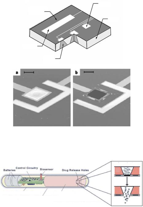
214 |
BABAK ZIAIE |
a
Anode
Silicon nitride or dioxide
Silicon
Cathode
Active substance
a |
|
b |
FIGURE 10.5. MicroCHIP drug delivery chip (top), a reservoir before and after dissolution of the gold membrane (bottom) [52].
Cross Section
|
Control Circuitry |
|
|
|
|
|
|
|
Biosensor |
|
|||
Batteries |
|
|
Drug Release Holes |
|||
|
||||||
|
|
|
|
|||
|
|
|
|
|
|
Artificial Muscle Membrane Drug Reservoir
Biocompatible Permeable Membrane
Close-Up of Drug Release Holes 
FIGURE 10.6. Schematic of the ChipRx smart drug delivery capsule. (Courtesy ChipRx)
IMPLANTABLE WIRELESS MICROSYSTEMS |
215 |
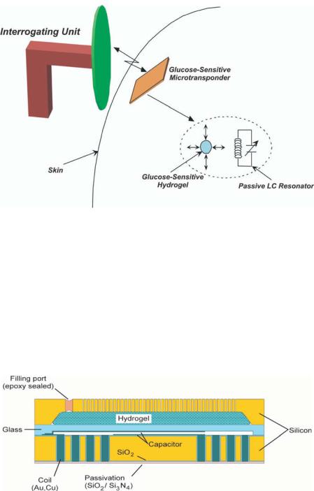
FIGURE 10.7. Basic concept behind the glucose-sensitive microtransponder.
sphincter, opening and closing a tiny reservoir. Due to the potency of many drugs, safety and regulatory issues are more stringent in implantable drug delivery microsystems and will undoubtedly delay their appearance in the clinical settings.
Figure 10.7 shows the basic concept behind the glucose-sensitive microtransponder [56]. A miniature MEMS-based microdevice is implanted in the subcutaneous tissue and an interrogating unit remotely measures the glucose levels without any hardwire connection. The microtrasponder is a passive LC resonator, which is coupled to a glucose-sensitive hydrogel. The glucose-dependent swelling and de-swelling of the hydrogel is coupled to the resonator causing a change the capacitor value. This change translates into variations of the resonant frequency, which can be detected by the interrogating unit. Figure 10.8 shows
FIGURE 10.8. Cross section of glucose microtransponder.
216 |
BABAK ZIAIE |
Coil
Capacitor
Glass
Silicon
 Coil
Coil
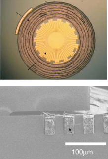
FIGURE 10.9. Optical micrograph and SEM cross section of glucose sensitive microtransponders.
the schematic drawing of the micro-transponder with a capacitive sensing mechanism. The glucose sensitive hydrogel is mechanically coupled to a glass membrane and is separated from body fluids (in this case interstitial fluid) by a porous stiff plate. The porous plate allows the unhindered flow of water and glucose while blocking the hydrogel from escaping the cavity. A change in the glucose concentration of the external environment will cause a swelling or de-swelling of the hydrogel, which will deflect the glass membrane and change the capacitance. The coil is totally embedded inside the silicon and can achieve a high quality factor and hence increased sensitivity by utilizing the whole wafer thickness (reducing the series resistance). The coil-embedded silicon and the glass substrate are hermetically sealed using glass-silicon anodic bonding. Figure 10.9 shows the optical micrograph of several devices and an SEM cross section showing the glass membrane and embedded coil.
10.5. REHABILITATIVE MICROSYSTEMS
Rehabilitative microsystems are used to substitute a lost function such as vision, hearing, or motor activity. In this category, we will describe two microsystems. The first one is a single channel neuromuscular microstimulator used to stimulate paralyzed muscle groups in paraplegic and quadriplegic patients. The second microsystem is a visual prosthetic device designed to stimulate ganglion cells in retina in order to restore vision to people afflicted with macular degeneration or retinitis pigmentosa.
Figure 10.10 shows a schematic of the single channel microstimulator [25]. This device is 10 × 2 × 2 mm3 in dimensions and receives power and data through an inductively coupled link. It can be used to stimulate paralyzed muscle groups using thin-film microfabricated