

Biomolecular Sensing Processing and Analysis - Rashid Bashir and Steve Wereley
.pdf94 |
NAM-TRUNG NGUYEN |
significantly improve the efficiency with smaller samples, fast response time, and higher analytical performance. However, the major drawback of silicon-based BMMDs is their cost. BMMDs for diagnostics and drug delivery are often used as disposable tools in medical treatments due to contamination hazards. Furthermore, compared to their microelectronic and micro electromechanical counterparts, BMMDs such as microfluidic devices have a relatively large size. The single use and the high material cost as well as the high processing cost in clean rooms make silicon-based BMMDs less attractive for the mass market.
Furthermore, silicon as a substrate material is not very compatible to biomedical applications. Many disposable biomedical gadgets were made of polymers. Thus, fully polymeric BMMDs promise to solve the problems of biocompatibility, and in addition offer a much lower total cost compared to their silicon counterparts. In the past few years, a number of devices were fabricated successfully using different polymers such as polydimethlsioxane (PDMS), polystyrene (PS), polyethylene (PT), polyethyleneterephthalate (PET), polycarbonate (PC), SU-8 and polymethylmethacrylate (PMMA). This chapter focuses on polymeric micro technologies, which promise the mass fabrication of BMMDs at a reasonable cost.
In contrast to conventional MEMSs, BMMDs have direct interactions with a biological environment. These interactions lead to implication for the proper operation of the devices. For instance, proteins and micro organisms tend to adsorb to synthetic surfaces [11]. The adsorbed layer creates malfunction in sensing applications and reduces the overall life span of the device. The use of BMMDs in biological environment not only affects the device itself, but also triggers a cellular response in the host [3]. Thus, the use of materials and the fabrication technology for BMMDs should consider the biocompatibility tailored to a application. Responsible agencies such as the Food and Drug Administration (FDA) only approve BMMDs for specific purposes and not the devices themselves in isolation. This chapter should read the different aspects of biocompatibility in material choice and fabrication technologies.
While numerous research works focused on the fabrication and the functionality of BMMDs, little was done on packaging and interconnection problems of these devices. Critical issues are biocompatibility of the package and microfluidic interconnects. The biological environment leads to special requirements in interfacing BMMDs with the surrounding wold. These requirements should be considered carefully in the design and the fabrication of BMMDs.
5.2. MATERIALS FOR BIOMEDICAL MICRO DEVICES
5.2.1. Silicon and Glass
Silicon is undoubtedly the most popular material in MEMS applications. Silicon micromachining technologies are established and well known [23, 26]. Single crystalline silicon wafers with high purity and different orientations are commercially available at a reasonable cost. The two basic micromachining techniques are bulk micromachining and surface micromachining. The deposition of a number of functional layers such as polysilicon, silicon dioxide, silicon nitride, metals and several organic layers is also well established. A variety of microdevices can be designed and fabricated by combining these techniques. In fact, all conventional MEMSs are silicon-based.
FABRICATION ISSUES OF BIOMEDICAL MICRO DEVICES |
95 |
{100} |
{111} |
|
(a) |
(b) |
|
(c)
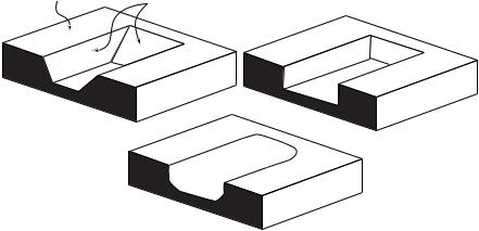
FIGURE 5.1. Etch profiles with different bulk micromaching techniques: (a) Anisotropic wet etching of silicon,
(b) Deep reactive ion etching (DRIE) of silicon or wet etching of photo sensitive glasses, (c) Isotropic etching in silicon or glass.
Glass consists of silicon oxide and oxides of metals. The amount of silicon oxide varies and depends on the glass type (68% in soda-lime glass, 81% in boronsilicate glass and almost 100% in fused silica) [4]. Analytical instruments in the past are widely based on glass wares. The reasons for the use of glass include high mechanical strength, high chemical resistance, high electrical insulation and a wide optical transmission range. Thus, glass was the first choice for fabricating BMMDs in diagnosis applications such as electrophoresis [6, 9, 30, Jacobson et al., 1994] electrochromatography [Jacobson et al., 1994] and DNA separation [37]. Most of the glasses can be etched in a buffered hydrofluoric acid (HF) solution [32] using a photo resist etch mask such as AZ 4620 [19]. The typical result of isotropic etching in glass is shown in Fig. 5.1c.
Glass can also be structured with photo lithography. Commercially available glasses such as Foturan [13] and FS21 [29] belong to this glass type. These glasses consist of silicon oxide, aluminum oxide and lithium oxide. The photo sensitivity is activated by doping the glass with oxides of elements such as Ag, Ce, Sn, Sb [29] For machining, the glass is exposed to ultraviolet radiation. The amorphous glass crystallizes under UV-exposure. The crystallized area can be removed selectively by a subsequent etch process in hydrofluoric acid. Wet etching of photo sensitive glass can result in straight walls similar to deep reactive etching (DRIE) of silicon, Fig. 5.1b.
5.2.2. Polymers
As already mentioned in the introduction, silicon-based and glass-based BMMDs have the drawbacks of higher cost and biocompatibility problems. Regarding a cheaper mass production of BMMDs, polymers offer a real alternative to silicon-based and glassbased substrates. Polymers are macromolecular materials, which are formed through polymerization reactions. In this reaction, the monomer units connect each other either in linear chains or in three-dimensional network chains and form a macromolecule. Based
96 |
NAM-TRUNG NGUYEN |
on their properties synthetic polymers can be categorized as thermoplastics, elastomers, and thermosets [5].
Polymers as functional materials fulfill a number of requirements of BMMDs [31]:
–Polymers are suitable for micro machining, the different micro fabrication techniques are discussed in section 5.3.
–Many polymers are optically transparent. Due to the requirement of optical detection methods such as fluorescence, UV/Vis absorbance, or Raman method, the device material should allow a wide optical transmission range and have a minimum autofluorescence.
–Many polymers are chemically and biologically compatible. The materials used in BMMDs should be inert to a wide range of solvents.
–Most polymers are good electrical insulators. An electrically insulating substrate is required in applications with a strong electrical field such as electrophoretic separation. In addition, good thermal properties are also desired due to thermal load resulting from Joule heating.
–The surface chemistry of polymers can be modified for a certain application.
The following sections discuss the properties of some typical polymers, which are frequently used in recently published works on BMMDs.
5.2.2.1.PMMA PMMA is known under trade names such as Acrylic, Oroglass, Perspex, Plexiglas, and Lucite. PMMA is available commercially in form of extrusion sheets. For micromachining purposes such as X-ray exposure, PMMA can be applied on a handling substrate by different ways: multilayer spin coating, bonding of a prefabricated sheet, casting, and plasma polymerization.
PMMA is one of the thermoplastic polymers. Thermoplastic polymers are usually linear-linked and will soften when heated above glass transition temperature. It can be reheated and reshaped before hardening in its form for many times. Thermoplastic polymers can be crystalline or amorphous. In general, transparent polymers are non-crystalline and translucent polymers are crystalline. PMMA has a non-crystalline structure. Thus, it has optical properties with a 92% light transmittance. PMMA also offers other excellent properties such as low frictional coefficient, high chemical resistance, and good electrical insulation. Thus PMMA is a good substrate for microfludic devices especially in biomedical applications.
The surface properties of PMMA can be modified chemically to suit its application [10] PMMA can be machined in many ways: X-ray exposure and subsequent developing, hot embossing, and laser machining (see section 5.3).
5.2.2.2.PDMS PDMS is a polymer that has an inorganic siloxane backbone with methyl groups attached to silicon. The prepolymers and curing agents of PDMS are both commercially available. PDMS is suitable for BMMDs with microchannels for biological samples in aqueous solutions. PDMS presents the following excellent properties [24]:
–PDMS can be micro machined using replica molding. The elastomeric characteristic allows PDMS to conform to nonplanar surfaces. PDMS can be released from a mold with delicate micro structures without damaging them and itself.
FABRICATION ISSUES OF BIOMEDICAL MICRO DEVICES |
97 |
–PDMS is optically transparent down to a wavelength of 280 nm, thus this material is suitable for devices utilizing UV detection schemes.
–PDMS is biocompatible, mammalian cells can be cultured directly on this material and PDMS devices can be implanted in a biological environment.
–PDMS can bond itself to a number of materials reversibly. Irreversible seal can be achieved by covalent bonds, if the contact surface is treated with oxygen plasma.
–PDMS surface is hydrophobic. An oxygen plasma treatment makes the surface hydrophilic and negatively charged, thus suitable for electrokinetic applications. Oxidized PDMS can also absorb other polymers, which modify the surface properties.
5.2.2.3. SU-8 Microstructures can be transferred to most polymers by hot embossing or replica molding. Direct photo lithography is possible with PMMA using X-ray. However, the X-Ray source and the corresponding mask are expensive and not suitable for mass production. SU-8 is a thick film resist, which allows photo lithography with high aspect ratios using conventional exposure equipments with near-UV wavelengths from 365 nm to 436 nm. Film thickness up to 2 mm and aspect ratios better than 20 can be achieved with SU-8.
SU-8 photoresist consists of three basic components:
–An epoxy resin, which has one or more epoxy groups. An epoxy group is referred to as the oxygen bridge between two atoms. During the polymerization process, epoxy resins are converted to a thermoset form of a three-dimensional network.
–A solvent such as gamma-butyrolacetone (GBL). The SU-8 2000 family (MicroChem Corp., USA) uses cyclopentanone (CP) as the solvent.
–A photoinitiator such as triarylium-sulfonium salt.
The unexposed SU-8 can be dissolved with solvent-based developers. The commercially available developer for SU-8 is propylene-glycol-methyl-ether-acetate (PGMA) (MicroChem Corp., USA).
SU-8 is chemically stable and is resistant to most acids and other solvents. The good mechanical properties allow the use of SU-8 directly as moveable components, section 5.3.1.1
5.3. POLYMERIC MICROMACHINING TECHNOLOGIES
5.3.1. Lithography
Lithography is the most important techniques for fabricating micro structures. Several lithography techniques were established during the development of microelectronics. Based on the type of the energy beam, lithography can be categorized as photolithography, electron lithography, X-ray lithography, and ion lithography [34]. The lithography process only allows transferring two-dimensional lateral structures. The desired pattern is transferred from a mask to the resist. In microelectronics and silicon-based MEMS-technology, the patterned resist is in turn the mask for transferring the pattern further into a functional layer. In polymeric micromachining, the structured resist can be used directly as the functional material or as a mold for replica molding of other polymers.
98 |
NAM-TRUNG NGUYEN |
A conventional lithography process consists of three basic steps:
–Positioning: lateral positioning and gap adjusting between the mask and the substrate,
–Exposure: exposure to the energy beam, transferring pattern by changed properties of the exposed area,
–Development: selective dissolution or etching of the resist pattern.
5.3.1.1. Lithography of Thick Resists Lithography of PMMA requires collimated X-ray with wavelength ranging from 0.2 nm to 2 nm. These high-energy beams are only available in synchrotron facilities. X-ray lithography also requires special mask substrates such as beryllium and titanium. The absorber material of a X-ray mask are heavy metals such as gold, tungsten , or tantalum. For a higher aspect ratios of the PMMA structures, high X-ray energy and consequently a thicker absorber layer are required. During the exposure to X-ray, the polymer chains in the exposed area are broken. Thus the exposed area can subsequently etched away by a developer. A typical developer consists of a mixture of 20 vol% tetrahydro-1, 4-oxazine, 5 vol% 2-aminoethanol-1, 60 vol% 2-(2-butoxy-ethoxy) ethanol, and 15 vol% water [7].
In contrast to the expensive X-ray lithography of PMMA, SU-8 only requires conventional UV-exposure equipment. A standard SU-8 process consists of several steps:
–Spin coating: SU-8 is commercially available with a variety of viscosities. At the same spin speed, a higher viscosity will result in a thicker film. The film thickness can also be adjusted by the spin speed.
–Soft bake: Before exposure the solvent is evaporated in the soft bake process. This
process can be carried out in a convection oven or on a hot plate. Ramping from 65 ◦C to 95 ◦C is recommended for this step.
–Exposure: Since the optical absorption of SU-8 increases sharply bellow the wavelength of 350 nm, the exposure should be carried out at wavelengths higher than this value. I-line equipment with mercury lamp is suitable for this step. The thicker the SU-8 layer, the higher is the required exposure dosage.
–Post exposure bake: After the exposure step, the SU-8 layer is selectively cross-linked by a thermal process. A two-step ramp between 65 ◦C to 95 ◦C is recommended to minimize the film stress and possible cracks. Rapid cooling after the thermal treatment should be avoided.
–Developing: The unexposed areas of the SU-8 film can be dissolved by immersion in a solvent-based developer.
–Hard bake: Another baking process after developing allows the remaining SU-8 to further cross-link and harden.
–Remove: Since polymerized SU-8 is resistant to most acids and other solvents, it’s very difficult to remove a cross-linked film after exposure. Measures such as etching in a strong acid solution, reactive ion etching in oxygen plasma or laser ablation can be used to remove polymerized SU-8.
5.3.1.2. SU-8 on PMMA Technique SU-8 can be used for forming microchannels on silicon and glass. A number of silicon-based and glass-based techniques were summarized
FABRICATION ISSUES OF BIOMEDICAL MICRO DEVICES |
99 |
in [26]. In this section, the fabrication of SU-8 on a polymer substrate is presented. The technique shows the possibility of fabrication of fully polymeric BMMDs.
In preparation for the process, a 3-mm-thick PMMA sheet was cut into 100-mm- diameter circular wafer using CO2-laser machining (section 5.3.4). The two films protecting the PMMA were kept intact to prevent dust and oil contamination during the cutting process. These protecting films were peeled off just before the SU-8 process. The wafer was cleaned with isopropyl alcohol (IPA) and deionized (DI) water. Strong solvents such as acetone should not be used for the cleaning process due to possible damage of the PMMA surface. Next, the wafer was dried in a convection oven at 90 ◦C for 30 minutes. PMMA has a low glass transition temperature at around 106 ◦C, so all baking temperatures should be kept under 90 ◦C.
Next, four milliliters of SU-8 2050 (Microchem Corp, USA) was dispensed onto the PMMA wafer. Spin-coating the resist at 500 rpm for 15 s, followed by 3000 rpm for 15 s produced a 50 mm thick film. This film acted as the base for the next SU-8 structural layer. The resist was soft-baked in the convection oven at 65 ◦C in 2 minutes, then at 90 ◦C in 15 minutes, and allowed to cool down to the room temperature of 24 ◦C, Fig. 5.2a. Subsequently, the resist was blanket-exposed to UV light (EV620 Mask aligner, EV Group) with an energy density of 525 mJ/cm2. The resist underwent hard baking at 65 ◦C in 2 minutes and at 90 ◦C in 5 minutes. Subsequently, a relaxation step at 65 ◦C, in 2 minutes was performed to release thermal stress in the SU-8 film, Fig. 5.2b.
In the next step, four milliliters of SU-8 2100 was dispensed onto the first SU-8 layer. The spinning speed was ramped up in 5 seconds to 500 rpm, held for 5 seconds, ramped up in 10 seconds to 2100 rpm, held for 22 seconds, and ramped down to full stop in 20 seconds.
SU-8 2050, 50 m PMMA substrate
(a)
UV source
(b)
(f)
SU-8 2100, 100 m
(c)
Mask
(d)
Channel structure
(e) |
(g) |
FIGURE 5.2. The SU-8 on PMMA process.
100 |
NAM-TRUNG NGUYEN |
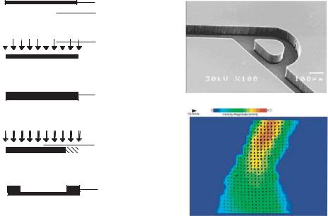
This recipe gave a 100-mm-thick film. The resist was soft baked for 10 minutes at 65 ◦C and for 40 min at 90 ◦C, Fig. 5.2c. After cooling down to room temperature, the second SU-8 layer was exposed with an energy density of 525 mJ/cm2 through a photo mask defining the desired structures, Fig. 5.2d. Next, a two-step hard bake was performed at 65 ◦C for 5 minutes and at 90 ◦C for 20 minutes. An intermediate step at 65 ◦C for 2 minutes was introduced to release the thermal stress in the SU-8 film. The SU-8 was developed in the PGMEA developer for 10 minutes. The wafer was then blown dry with nitrogen, Fig. 5.2e. Figure 5.2f shows a Tesla-valve fabricated with the above technology. After sealing with a second PMMA wafer, covered with 5-µm-thick SU-8, the channel structure was tested using micro particle image velocimetry (micro-PIV). The results show and excellent seal with high-quality microchannels, Fig. 5.2g. Circular wafer is preferred for the SU-8-on-PMMA process because it reduces the excessive edge bead associated with a rectangular wafer during the coating process. In our first experiments, rectangular wafers were used. The rectangular shape resulted in very thick beads at the four edges. The edge bead was even thicker at the four corners. This excessive edge bead prevented the photo mask to properly contact with the majority of the resist surface during exposure, causing poor lithography resolution.
In some of the first experiments, the structural SU-8 was directly coated on to the PMMA wafer. After developing, a layer of undeveloped SU-8 still remained on the wafer. The residual SU-8 could not be cleaned off by IPA, DI water, or even acetone. An ultrasonic bath treatment did remove some of the residual, but part of the SU-8 structure was also damaged. It can be concluded that the residual could not be removed by normal procedures. The solution was to coat a base SU-8 layer as described in the previous section.
The thermal expansion coefficients (TEC) of PMMA and SU-8 are 60 ppm/◦C and 52 ppm/◦C, respectively. These matching properties result in less crack in the SU-8 film, and a better film adhesion on wafer. Thus, it is possible to use PMMA as the handling substrate for the polymeric surface micromachining techniques presented in section 5.3.2.
5.3.2. Polymeric Surface Micromachining
Polymeric surface micromachining technique is similar to its silicon-based counterpart. A functional layer is structured on top of a sacrificial layer. Removing the sacrificial layer results in a freely moveable structure. Polymers can work as both sacrificial layer and functional layer. With SU-8 as the functional layer, polymers such as polystyrene [22] or metals such as chromium [27] were used as sacrificial layers. In the following section a process with silicon directly as sacrificial material as well as the handling substrate is demonstrated by the fabrication of a polymeric micropump [35] and a polymeric microgripper.
5.3.2.1. Polymeric Micropump The micropump consists of different layers made of PMMA and SU-8. Double-sided adhesive tapes act as bonding layers. All layers have the form of a disc with 1-cm diameter. Easy assembly can be achieved using alignment holes machined in all layers and alignment pins. The PMMA-parts and the adhesive tapes are cut and drilled by the CO2-laser (section 5.3.4).
Because of the required high accuracy, the micro checkvalves were fabricated in a 100-µm-thick SU-8 layer (SU8 2100, Microchem Corp.) by photo lithography. The process is similar to that described in section 5.3.1.2. Here, a silicon wafer was used as both the handler wafer and the sacrificial material.
FABRICATION ISSUES OF BIOMEDICAL MICRO DEVICES
(a)
(b)
(c) |
101
SU-8
1.mask
2.mask
SU-8
(d)
(e)
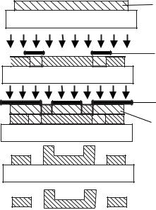
FIGURE 5.3. Steps of a two-layer polymeric surface micromachining process for making a microvalve.
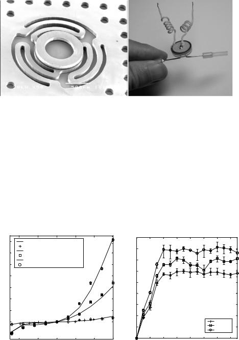
The SU-8 process started with coating of the first SU-8 layer, Fig. 5.3a. The first lithography mask contains the valve disc and the valve springs, Fig. 5.3b. A second SU-8 layer was coated and structured using another mask to form the sealing ring on the valve disc, Fig. 5.3c. Both SU-8 layers were developed and hard-baked in the same process, Fig. 5.3d. Etching the silicon substrate in a KOH solution at room temperature releases the SU-8 valve discs, Fig. 5.3e. Tiny circular holes incorporated on the SU-8 disc avoid micro cracks and work as etch access for faster release. Figure 5.4a shows the fabricated SU-8 micro check valve.
The pump actuator is a commercially available piezoelectric bimorph disc that is bonded on the assembled pump stack by the same adhesive tape. The assembly process was carried out at a room temperature of 25 ◦C. The inlet and outlet of the micropump are stainless steel needles of 600-µm outer diameter. The needles are glued on the inlet/outlet holes of the pump body. The assembled pump is depicted in Fig. 5.4b. The micro checkvalves and the micropump were successfully tested with water. Figure 5.5a shows the characteristics of microvalves with different spring lengths. A valve with longer spring arms will be softer, thus allowing a higher flow rate at the same pressure. The behavior of the microvalves also affect the characteristics of the micropumps as shown in Fig. 5.5b. Micropumps with softer valves can deliver a higher flow rate at the same actuating frequency and voltage.
5.3.2.2. Polymeric Microgripper Microgrippers have been one of the typical applications of MEMS-technology. Microgrippers were developed for systems, which can handle microparts or manipulate cells. For the latter application, bio-compatibility and gentle handling are often required. The microgripper reported here was fabricated using polymeric surface micromachining with SU-8 as the structural material and silicon as the sacrificial
102 |
NAM-TRUNG NGUYEN |
(a) |
(b) |
FIGURE 5.4. Fabrications results: (a) the microvalve (b) the assembled micropump.
material. A titanium/platinum layer work as the heater for the gripper. The relatively low operating temperature of less then 100 ◦C and the gentle gripping force make the gripper suitable for applications with living cells and bacteria.
The thick-film resist SU-8 has an unique property, that it does not soften at elevated temperatures. Higher temperatures cause better cross-links and make SU-8 even harder. Thus, SU-8 is suitable for the use with thermal actuators. Since SU-8 is not conductive, a thin titanium/platinium on top of the SU-8 structure was used as the heater. Due to the large ratio between the thickness of the metal layer (hundred nanometers) and the SU-8 part (one hundred microns), vertical bending due to thermomechanical mismatch is negligible compared to lateral bending. With an Young’s modulus of 4.02 GPa [21] SU-8 is almost
Flow rate ( L/min)
1400
1200
1000
800
600
400
200
0
|
Simulation, Valve 1, 5mm gap |
|
|
|
1800 |
|
|
|
|
|
|
|
||
|
|
|
|
|
|
|
|
|
|
|
|
|||
|
Measurement, Valve 1 |
|
|
|
|
1600 |
|
|
|
|
|
|
|
|
|
Simulation, Valve 1, 12mm gap |
|
|
|
|
|
|
|
|
|
|
|||
|
|
|
|
|
|
|
|
|
|
|
|
|||
|
Measurement, Valve 2 |
|
|
|
|
1400 |
|
|
|
|
|
|
|
|
|
Simulation, Valve 1, 12mm gap |
|
|
|
|
|
|
|
|
|
|
|||
|
Measurement, Valve 3 |
|
|
|
|
|
|
|
|
|
|
|
|
|
|
|
|
|
|
|
L/min) |
1200 |
|
|
|
|
|
|
|
|
|
|
|
|
|
1000 |
|
|
|
|
|
|
|
|
|
|
|
|
|
|
( |
|
|
|
|
|
|
|
|
|
|
|
|
|
|
|
|
|
|
|
|
|
|
|
|
|
|
|
|
|
rate |
800 |
|
|
|
|
|
|
|
|
|
|
|
|
|
Flow |
|
|
|
|
|
|
|
|
|
|
|
|
|
|
600 |
|
|
|
|
|
|
|
|
|
|
|
|
|
|
|
|
|
|
|
|
|
|
|
|
|
|
|
|
|
|
400 |
|
|
|
|
|
|
|
|
|
|
|
|
|
|
|
|
|
|
|
|
Pump 1 |
|
|
|
|
|
|
|
|
200 |
|
|
|
|
|
Pump 2 |
|
|
|
|
|
|
|
|
|
|
|
|
|
Pump 3 |
||
|
|
|
|
|
|
|
|
|
|
|
|
|
||
|
|
|
|
|
|
|
0 |
|
|
|
|
|
|
|
-4000 |
-2000 |
0 |
2000 |
4000 |
6000 |
|
0 |
20 |
40 |
60 |
80 |
100 |
120 |
140 |
|
|
Pressure (Pa) |
|
|
|
|
|
|
Frequency (Hz) |
|
|
|
||
(a) |
(b) |
FIGURE 5.5. Characteristics of the microvalves (a) and the micropumps (b).
FABRICATION ISSUES OF BIOMEDICAL MICRO DEVICES
(a)
(b)
Mask
(c)
(d)
 Stencil
(e)
Opening for bond pads
Opening for gripper area
(f) |
|
1000 200 |
SU-8 |
Si |
Pt/Ti (g) |
FIGURE 5.6. The polymeric microgripper: (a) the fabrication steps (b) the design.
103
4000
1000
40 times softer than silicon, while its thermal expansion coefficient of 52 ± 5 × 10⁻⁶/K [21] is superior to that of silicon (2.4 × 10⁻⁶/K [12]). Thus, SU-8 microgripper with thermal actuator offers a much lower operating temperature, lower power and more gentle handling force than its silicon counterparts.
The fabrication process consists of three basic steps: fabrication of the SU-8 gripper, deposition of the titanium/platinum layer, and release. The SU-8 body was fabricated with the polymeric surface micromaching techniques described in section 5.3.2.1. Silicon was used directly as sacrificial material, Fig. 5.6a. The process started with spin-coating SU-8 2100 photoresist (Microchem Corp., USA) on silicon, Fig. 5.6b. This SU-8 layer was then soft baked and exposed to UV light using a mask defining the SU-8 part, Fig. 5.6c. The intended thickness of this SU-8 film was 100 µm. After hard baking, the SU-8 layer was allowed to cool down to room temperature. They were then developed with propylene glycol methyl ether (PGMEA), Fig. 5.6d.
In preparation for the second step, a stencil was dry-etched though a silicon wafer using DRIE. The stencil only defines the bonding pads for the heaters. The heater structures themselves are defined masklessly by the SU-8 structure. Thus the entire gripper body was exposed to the subsequent evaporation processes. Next, the stencil wafer was positioned to the handler wafer containing the developed SU-8 parts. The two wafers are fixed using adhesive tapes. Subsequently, a 50-nm thick titanium layer was evaporated through the stencil. Titanium works as the adhesion layer between SU-8 and the subsequent platinum layer. A 70-nm thick platinum layer was evaporated on top of the titanium layer, Fig. 5.6e.
In the final step, the SU-8 microgrippers covered by the metal double layer were released in 30% KOH solution. Etch access created by many circular holes on the discs