

Biomolecular Sensing Processing and Analysis - Rashid Bashir and Steve Wereley
.pdf32 |
MIN YUE, ARUN MAJUMDAR, AND THOMAS THUNDAT |
for studying all reactions. Furthermore, it is a label-free approach, which can be easily multiplexed to study thousands of reactions simultaneously. In this chapter, we discuss the latest developments in the technology of cantilever arrays and how it can be used to study specific biomolecular reactions involving nucleic acids and proteins.
REFERENCES
[1]P. Angenendt, J. Glokler,¨ Z. Konthur et al. 3D protein microarrays: performing multiplex immunoassays on a single chip. Anal. Chem., 75:4368–4372, 2003.
[2]P. Arenkov, A. Kukhtin, A. Gemmell, S. Voloshchuk, V. Chupeeva, and A. Mirzabekov. Protein microchips: use for immunoassay and enzymatic reactions. Anal. Biochem., 278:123, 2000.
[3]Y. Arntz, J.D. Seelig, H.P. Lang, J. Zhang, P. Hunziker, J.P. Ramseyer, E. Meyer, M. Hegner, and C. Gerber. Label-free protein assay based on a nanomechanical cantilever array. Nanotechnology, 14:86, 2003.
[4]R. Berger, E. Delamarche, H. Lang, C. Gerber, J. K. Gimzewski, E. Meyer, and H. J. Guntherodt,¨. Surface stress in the self-assembly of alkanethiols on gold. Science, 276:2021, 1997.
[5]H.J. Butt. A sensitive method to measure changes in surface stress of solids. J. Coll. Inter. Sci., 180:251, 1996.
[6]G.Y. Chen, T. Thundat, E. A. Wachter, and R.J. Warmack. Adsorption-induced surface stress and its effects on resonance frequency of microcantilevers. J. Appl. Phys., 77(8):3618, 1995.
[7]J. Fritz, M.K. Baller, H.P. Lang, H. Rothuizen, P. Vettiger, E. Meyer, H.J. Guntherodt,¨ C. Gerber, and J.K. Gimzewski. Translating biomolecular recognition into nanomechanics. Science, 288:316, 2001.
[8]H. Ge. UPA, a universal protein array system for quantitative detection of protein-protein, protein-DNA, protein-RNA and protein-ligand interactions. Nucleic Acids Res., 28:e3, 2000.
[9]D. Guschin, G. Yershov, A. Zaslavsky et al. Manual manufacturing of oligonucleotide, DNA, and protein chips. Anal. Biochem., 250:203, 1997.
[10]B.B. Haab, M.J. Dunham, and P.O. Brown. Protein microarrays for highly parallel detection and quantitation of specific proteins and antibodies in complex solutions. Genome Biol., 2:R4, 2001.
[11]M.F. Hagan, A. Majumdar, and A.K. Chakraborty. Nanomechanical forces generated by surface grafted DNA
J.Phys. Chem. B, 106:10163, 2002.
[12]K. Hansen, H. Ji, G. Wu, R. Datar, R. Cote, and A. Majumdar. Cantilever-based optical deflection assay for discrimination of DNA single-nucleotide mismatches. Anal. Chem., 73:1567, 2001.
[13]R.-P. Huang, R. Huang, Y. Fan, and Y. Lin. Simultaneous detection of cytokines from conditioned media and patient’s sera by an antibody-based protein array system. Anal. Biochem., 294:55, 2001.
[14]H.P. Lang, R. Berger, C. Andreoli, J. Brugger, M. Despont, P. Vettiger, Ch. Gerber, and J.K. Gimzewski. Sequential position readout from arrays of micromechanical cantilver sensors. Appl. Phys. Lett., 72:383, 1998.
[15]T.O. Joos, M. Schrenk, P. Hopfl,¨ K. Kroger, U. Chowdhury, D. Stoll, D. Schorner,¨ M. Durr,¨ K. Herick,
S.Rupp, K. Sohn, and H. H¨ammerle. A microarray enzyme-linked immunosorbent assay for autoimmune diagnostics. Electrophoresis, 21:2641, 2000.
[16]V. Knezevic, C. Leethanakul, V.E. Bichsel, J.M. Worth, V.V. Prabhu, J.S. Gutkind, L.A. Liotta, P.J. Munson, E.F. Petricoin, and D.B. Krizman. Proteomic profiling of the cancer microenvironment by antibody arrays. Proteomics, 1:1271, 2001.
[17]G. MacBeath and S.L. Schreiber. Printing proteins as microarrays for high-throughput function determination. Science, 289:1760, 2000.
[18]R. Marie, H. Jensenius, J. Thaysen, C.B. Christensen, and A. Boisen. Adsorption kinetics and mechanical properties of thiol-modified DNA-oligos on gold investigated by microcantilever sensors. Ultramicroscopy, 91:29, 2002.
[19]R. McKendry, J. Zhang, Y. Arntz, T. Strunz, M. Hegner, H.P. Lang, M.K. Baller, U. Certa, E. Meyer, H.-
J.Guntherodt, and C. Gerber. Multiple label-free biodetection and quantitative DNA-binding assays on a nanomechanical cantilever array. Proc. Natl. Acad. Sci., 99:9783, 2002.
[20]T. Miyatani and M. Fujihira. Calibration of surface stress measurements with atomic force microscopy. J. Appl. Phys., 81:7099, 1997.
[21]R. Raiteri, G. Nelles, H.-J. Butt, W. Knoll, and P. Skl´adal. Sensing biological substances based on the bending of microfabricated cantilevers. Sens. Actu. B, 61:213, 1999.
CANTILEVER ARRAYS |
33 |
[22]C.A. Rowe, S.B. Scruggs, M.J. Feldstein, and J.P. Golden, Ligler. An array immunosensor for simultaneous detection of clinical analytes. Anal. Chem., 71:433, 1999.
[23]M.V. Salapaka, S. Bergh, J. Lai, A. Majumdar, and E. McFarland. Multimode noise analysis for scanning probemicroscopy. J. Appl. Phys., 81:2480, 1997.
[24]D. Sarid. Scanning Force Microscopy. Oxford University Press, New York, 1994.
[25]S. Satyanarayana, R. Karnik, and A. Majumdar. Stamp and stick room temperature bonding technique for microdevices. J. MEMS, (in press), 2004.
[26]G.G. Stoney. The tension of metallic films deposited by electrolysis. Proc. Roy. Soc. Lond. A, 82:172, 1909.
[27]J. Thaysen, A. Boisen, O. Hansen, and S. Bouwstra. Atomic force microscopy probe with piezoresistive read-out and a highly symmetrical Wheatstone bridge arrangement. Sens. Actuators A, 83:47, 2000.
[28]T. Thundat, R.J. Warmack, G.Y. Chen, and D.P. Allison. Thermal and ambient-induced deflections of scanning force microscope cantilevers. Appl. Phys. Letts., 64:2894, 1994.
[29]T. Thundat, P.I. Oden, and R.J. Warmack. Microcantilever sensors. Microscale Thermophys. Eng., 1:185, 1997.
[30]T. Thundat and A. Majumdar. Microcantilevers for physical, chemical, and biological sensing. In F.G. Barth, J.A.C. Humphrey, T.W. Seecomb, (eds.) Sensors and Sensing in Biology and Engineering. Springer-Verlag, New York, 2003.
[31]O.N. Tufte and E.L. Stelzer. Piezoresistive properties of silicon diffused layers. J. Appl. Phys., 34:323, 1993.
[32]E.A. Wachter and T. Thundat. Micromechanical sensor for chemical and physical measurements. Rev. Sci. Instrum., 66:3662, 1995.
[33]R. Wiese, Y. Belosludtsev, T. Powdrill et al. Simultaneous multianalyte ELISA performed on a microarray platform. Clini. Chem., 47(8):1451, 2001.
[34]G. Wu, H. Ji, K. Hansen, T. Thundat, R. Datar, R. Cote, M.F. Hagan, A.K. Chakraborty, and A Majumdar. Origin of nanomechanical cantilever motion generated from biomolecular interactions. Proc. Natl. Acad. Sci., 98:1560, 2001a.
[35]G. Wu, R. Datar, K. Hansen, T. Thundat, R. Cote, and A. Majumdar. Bioassay of prostate specific antigen (PSA) using microcantilevers. Nat. Biotechnol., 19:856, 2001b.
[36]M. Yue, H. Lin, D.E. Dedrick, S. Satyanarayana, A. Majumdar, A.S. Bedekar, J.W. Jenkins, and S. Sundaram. A 2-D microcantilever array for multiplexed biomolecular analysis. J. MEMS, 13:290, 2004a.
[37]M. Yue, J.C. Stachowiak, and A. Majumdar. Cantilever arrays for multiplexed mechanical analysis for biomolecular reactions. MCB, (in press), 2004b.
[38]M. Yue. High-Throughput Bioassays Based on Nanomechanics and Nanofluidics. Ph.D. Dissertation, University of California, Berkeley, in preparation, 2004.
[39]H. Zhu, J.F. Klemic, S. Chang, P. Bertone, A. Casamayor, K.G. Klemic, D. Smith, M. Gerstein, M.A. Reed, and M. Snyder. Analysis of yeast protein kinase using protein chips. Nat. Gene., 26:283, 2000.
3
An On-Chip Artificial Pore for Molecular Sensing
O. A. Saleh1 and L. L. Sohn2
1 Laboratoire de Physique Statistique, Ecole Normale Superieure,´ Paris, France 2 Dept. of Mechanical Engineering, University of California, Berkeley, CA. USA
3.1. INTRODUCTION
Currently, a variety of strategies for developing nanopores for molecular sensing exist— from engineering transmembrane protein pores so that they can detect sequence-specific DNA strands with single-base resolution [1, 2] to “drilling” molecular-scaled holes into silicon nitride membranes to detect the presence of single molecules of DNA [3, 4] to employing gold [5] or carbon [6] nanotubes as the ultimate artificial pores. While all of these strategies have shown early success in molecular sensing, there are major technological hurdles one must overcome: reproducibly creating an effective pore, maintaining a pore’s stability over a period of time, and integrating the pore into a device that is inexpensive and easy to fabricate and use. Here, we describe our group’s effort in developing a fullyintegrated artificial pore on chip for molecular sensing. As we will demonstrate, our pore addresses the technological hurdles with which other nanopore strategies are confronted. Equally important, we will show that our on-chip artificial pore is a flexible platform technology that has a number of diverse applications—from label-free immunoassays to single-molecule DNA sizing.
3.2. THE BASIC DEVICE: FABRICATION AND MEASUREMENT
The on-chip artificial pore we have developed is based on the Coulter counter technique of particle sizing [7]. Coulter counters typically consist of two reservoirs of particle-laden solution separated by a membrane and connected by a single pore through that membrane.
36 |
O. A. SALEH AND L. L. SOHN |
By monitoring changes in the electrical current through the pore as individual particles pass from one reservoir to another, a Coulter counter can measure the size of particles whose dimensions are on the order of the pore dimensions. While this method has long been used to characterize cells several microns in diameter [8, 9], its relative simplicity has led to many efforts to employ it to detect nanoscale particles [10, 11].
Our on-chip artificial pore was initially fabricated on top of a quartz substrate using standard microfabrication techniques [12]. We utilized a four-terminal measurement of the current through the pore. Because we are able to control precisely the pore dimensions (which we can easily measure using optical and atomic force microscopies), we can predict quantitatively the response of our pore to various-sized particles. We have fabricated pores with lateral dimensions between 400 nm and 1 µm, and used them to detect latex colloidal particles as small as 87 nm in diameter. As we will show, our device is easily integratable with other on-chip analysis systems.
3.2.1. Fabrication of the Pore
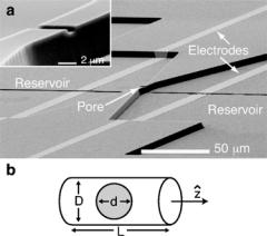
Our device, shown in Fig. 3.1, is fabricated in multiple stages. Each stage consists of lithographic pattern generation, followed by pattern transfer onto a quartz substrate using either reactive ion etching (RIE) or metal deposition and lift-off. The first stage is the fabrication of the pore. A line is patterned on the substrate using either photolithography (PL) for line widths ≥1 µm, or electron-beam lithography (EBL) for line widths between 100 and 500 nm, and then etched into the quartz using a CHF3 RIE. The substrate subsequently undergoes a second stage of PL and RIE to define two reservoirs that are 3.5 µm deep, separated by 10 µm, and connected to each other by the previously-defined channel. The length of the pore is defined in this second stage by the separation between the two reservoirs. The final stage consists of patterning four electrodes across the reservoirs, followed by two
FIGURE 3.1. (a) Scanning electron micrograph of our on-chip artificial pore. The 3.5 µm deep reservoirs and the inner Ti/Pt electrodes, which control the voltage applied to the pore but pass no current, are only partially shown. The outer electrodes, which inject current into the solution, are not visible in this image. The inset shows a magnified view of this device’s pore, which has dimensions 5.1 × 1.5 × 1.0 µm3. (b) A schematic diagram of a spherical particle of diameter d in a pore of diameter D and length L. [From Ref. 12.]
AN ON-CHIP ARTIFICIAL PORE FOR MOLECULAR SENSING |
37 |
depositions of 50 Å/250 Å Ti/Pt in an electron-beam evaporator with the sample positioned 45 degrees from normal to the flux of metal to ensure that the electrodes are continuous down both walls of the reservoirs.
The device is sealed on top with a silicone-coated (Sylgard 184, Dow Corning Corp.) glass coverslip before each measurement. Prior to sealing, both the silicone and the substrate are oxidized in a DC plasma to insure the hydrophilicity [13] of the reservoir and pore and to strengthen the seal [14] to the quartz substrate. After each measurement, the coverslip is removed and discarded, and the substrate is cleaned by chemical and ultrasonic methods. Thus, each device can be reused many times.
3.2.2. Pore Measurement
We have measured solutions of negatively-charged (carboxyl-coated) latex colloids (Interfacial Dynamics, Inc.) whose diameters range from 87 nm to 640 nm using the device we just described. All colloids were suspended in a solution of 5x concentrated TBE buffer with a resistivity of 390 -cm and pH 8.2. To reduce adhesion of the colloids to the reservoir and pore walls, we added 0.05% v/v of the surfactant Tween 20 to every solution. The colloidal suspensions were diluted significantly from stock concentrations to avoid jamming of colloids in the pore; typical final concentrations were 108 particles/mL. The pore and reservoirs were filled with solution via capillary action.
The sensitivity of a Coulter counter relies upon the relative sizes of the pore and the particle to be measured. The resistance of a pore R p increases by δ R p when a particle enters since the particle displaces conducting fluid. δ R p can be estimated [9] for a pore aligned along the z-axis (see Fig. 3.2) by
δ R p = ρ |
A(z) − R p |
(3.1) |
|
d z |
|
where A(z) represents the successive cross sections of the pore containing a particle, and ρ is the resistivity of the solution. For a spherical particle of diameter d in a pore of diameter D and length L, the relative change in resistance is
R pp |
= |
L |
|
1 |
(d/D2) |
|
1/2 − |
D |
(3.2) |
δ R |
|
D |
arcsin(d/D) |
d |
|
||||
|
|
|
|
− |
|
|
|
|
|
Eqs. (3.1) and (3.2) assume that the current density is uniform across the pore, and thus is not applicable for cases where the cross section A(z) varies quickly, i.e. when d D. For that particular case, Deblois and Bean [10] formulated an equation for δ R p based on an approximate solution to the Laplace equation:
R pp |
= LD2 |
|
2L2 + |
1 |
1 + (D/L)2 |
F |
D3 |
|
(3.3) |
δ R |
d3 |
|
D2 |
|
1 |
|
d3 |
|
|
where F (d3/D3) is a numerical factor that accounts for the bulging of the electric field lines into the pore wall. When employing Eq. (3.3) to predict resistance changes, we find
38 |
O. A. SALEH AND L. L. SOHN |
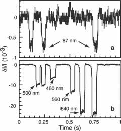
FIGURE 3.2. Relative changes in baseline current δI/I vs time for (a) a monodisperse solution of 87 nm diameter latex colloids measured with an EBL-defined pore of length 8.3 µm and cross section 0.16 µm2, and (b) a polydisperse solution of latex colloids with diameters 460, 500, 560, and 640 nm measured with a PL-defined pore of length 0.5 µm and cross section 1.2 µm2. Each downward pulse represents an individual particular entering the pore. The four distinct pulse heights in (b) correspond as labeled to the four different colloid diameters. [From Ref. 12.]
an effective value for D by equating the cross sectional area of our square pore with that of a circular pore.
If R p is the dominant resistance of the measurement circuit, then relative changes in the current I are equal in magnitude to the relative changes in the resistance, |δ I /I | = |δ R p /R p |, and Eqs. (3.2) and (3.3) can both be directly compared to measured current changes. This comparison is disallowed if R p is similar in magnitude to other series resistances, such as the electrode/fluid interfacial resistance, Re/ f , or the resistance Ru of the reservoir fluid between the inner electrodes and the pore. We completely remove Re/ f from the electrical circuit by performing a four-point measurement of the current (see Fig. 3.1a). We minimize Ru by placing the inner electrodes close to the pore (50 µm away on either side), and by designing the reservoir with a cross section much larger than that of the pore. For a pore of dimensions 10.5 µm by 1.04 µm2 we measured R p = 36 M , in good agreement with the 39 M value predicted by the pore geometry and the solution resistivity. This confirms that we have removed Ru and Re/ f from the circuit.
Fig. 3.2 shows representative data resulting from measuring a monodisperse solution of colloids 87 nm in diameter with an EBL-defined pore (Fig. 3.1a), and from measuring a polydisperse solution containing colloids of diameters 460 nm, 500 nm, 560 nm, and 640 nm with a PL-defined pore (Fig. 3.1b). Each downward current pulse in Fig. 3.2, corresponds to a single colloid passing through the pore. For the data shown, 0.4 V was applied to the pore. In other runs, the applied voltage was varied between 0.1 and 1 V to test the electrophoretic response of the colloids. We found that the width of the downward current pulses varied
AN ON-CHIP ARTIFICIAL PORE FOR MOLECULAR SENSING |
39 |
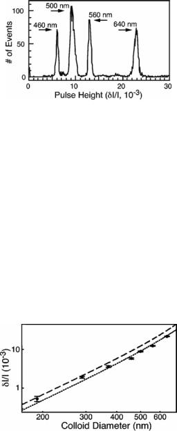
FIGURE 3.3. A histogram of pulse heights resulting from measuring the polydisperse solution shown in Figure 3.2(b). The resolution of this particular device is ±10 nm in diameter for the particles measured. [From Ref. 12.]
approximately as the inverse of the applied voltage, as is expected for simple electrophoretic motion.
Fig. 3.3 shows a histogram of 3000 events measured for the polydisperse solution. The histogram shows a very clear separation between the pore’s response to the differentlysized colloids. The peak widths in Fig. 3.3 represent the resolution of this device, which we find to be ±10 nm in diameter for the measured colloids. This precision approaches the intrinsic variations in colloid diameter of 2–4%, as given by the manufacturer. In this run, the maximum throughput was 3 colloids/s, a rate easily achievable for all of our samples. Event rates are limited by the low concentrations needed to avoid jamming.
We used a device whose pore size was 10.5 µm by 1.04 µm2 to measure colloids ranging from 190 nm to 640 nm in diameter. Figure 3.4 shows the comparison between the measured mean pulse heights and those predicted by Eqs. (3.2) and (3.3). As shown, there is excellent agreement between the measured and calculated values, with the measured error insignificant compared to the range of pulse heights. In addition, the measurements more
FIGURE 3.4. Comparison of measured δI/I values (circles) those predicted by Eq. (3.2) (dotted line) and Eq. (3.3) (dashed line). The measured data were taken over several runs on a single PL-defined pore of length 10.6 µm and cross section 1.04 µm2. Error bars for the larger colloid sizes are obscured by the size of the plotted point. As the colloid diameter increases, there is a transition from agreement with Eq. (3.3) to Eq. (3.2). This reflects the fact that the derivation of Eq. (3.3) assumes the colloid diameter d is much less than the pore diameter D; conversely Eq. (3.2) relies on an assumption that holds only as d approaches D, and breaks down for smaller colloids. [From Ref. 12.]
40 |
O. A. SALEH AND L. L. SOHN |
closely follow Eq. (3.3) for small d and Eq. (3.2) for larger D, as was anticipated in the derivation of those equations.
3.2.3. PDMS-Based Pore
In the initial work we have just described, we drove the particles through the pore electrophoretically, thus requiring the particles to carry a relatively high electrostatic charge for effective electric field-driven motion. Motivated by the desire to measure particles that are not highly charged, such as viruses or protein-coated colloids, we have developed a second version of the device that utilizes hydrostatic pressure to drive the particles through the pore. Here, we describe the fabrication of a pressure-driven pore and also discuss refinements we have made in the analysis of our data. These refinements, associated with off-axis particle effects, allow us to have higher precision when we determine the colloid size.
Figure 3.5 shows a picture of our modified device: a polydimethylsiloxane (PDMS) mold sealed to a glass coverslip. The PDMS mold is cast from a master [15] and contains two reservoirs (7 µm deep, 400 µm wide) connected to an embedded pore (typically 7–9 µm long and 1 µm in diameter). The glass coverslip has platinum electrodes that extend across the width of the reservoirs and are fabricated on the glass coverslip prior to PDMS sealing. These electrodes are used to perform the four-point electronic measurement. We prepare both the PDMS slab and the coverslip using standard lithographic, micro-molding, and metal deposition techniques. Solution is added to the reservoirs via two holes cut through the PDMS slab, and capillary action is used to initially draw the solution through both reservoirs and the pore. Pressure ( 1 psi) is applied to the access holes after loading the solution in order to drive the suspended latex colloids at a velocity of 200µm/sec through the pore.
The analysis of the pulses produced during pressure-driven flow is complicated by the effects of particles that travel off the pore’s central axis. Relative to particles of identical
Reservoir
Pore |
Top view |
|
Reservoir
Side view
PDMS
DNA
Glass
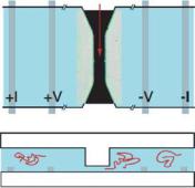
FIGURE 3.5. Schematic top and side views of our nanopore device, which consists of two 5 µm deep reservoirs connected by a lateral pore of 3 µm length and 200 nm diameter; an optical image of an actual pore sealed to a glass coverslip is incorporated into the top view. Molecules in the reservoirs are electrophoretically drawn through the pore, partially blocking the flow of ions. The current through the pore is measured using a four-terminal technique, where the voltage and current controlling platinum electrodes are as labeled. [From Ref. 37.]
AN ON-CHIP ARTIFICIAL PORE FOR MOLECULAR SENSING |
41 |
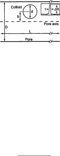
FIGURE 3.6. Schematic of the measurement geometry for a pore of diameter D and length L containing a colloid of diameter d that travels a distance b off the pore axis. Inset: Typical trace of the measured resistance vs time showing the passage of a single colloid that produces a resistance pulse of width τ and height R. [From Ref. 16.]
size that travel on-axis, off-axis particles take longer to transit the pore (causing wider pulses) and produce larger electrical resistance changes. The former effect, which we refer to as the hydrodynamic off-axis effect, is simply due to the parabolic distribution of fluid velocity within the pore. The latter effect, which we refer to as the electrical off-axis effect, occurs because off-axis particles enhance the non-uniformity in the distribution of electrical current density and consequently increase further the electrical resistance. Here, we discuss two main results [16]: first, we show how off-axis particles affect data taken on populations of colloidal particles and propose a method to remove these effects. Second, we point out that a device utilizing pressure-driven flow will have an increased resolution over one using electrophoretic flow, since the algorithm we have developed to remove off-axis effects can only be performed for pressure-driven flow. As we will demonstrate, both results should increase the precision of the resistive-pulse technique in future applications.
To describe quantitatively our data, we follow the work of Berge et al. [17] who formulated phenomenological equations to describe the two aforementioned off-axis effects. For the hydrodynamic effect, they found that previous experimental data [18] on the time τ for a particle to pass through the pore are well described by
τ = |
τ0 |
(3.4) |
(1 − x 2)(c1 − c2 x 5) |
where τ0 = 16η(L/D)2/ P is the on-axis transit time for an infinitely small particle, η is the fluid viscosity, L is the pore length, D is the pore diameter, P is the pressure drop across the pore, x = 2b/D is the fractional radial position for a particle centered a distance b off of the pore axis, c1 = 1 − (2/3)(d/D)2, c2 = 23.36(1 − c1), and d is the particle diameter (see Fig. 3.6). Berge et al. [17] then utilized Eq. 3.4 to describe empirically the variation in the change in electrical resistance R with an off-axis coordinate x as
R = R0 |
1 + α D |
|
(3.5) |
|
|
|
x d |
3 |
|
where R0(d, D, L) is the change in resistance for the on-axis particle (see Ref. 18 for its functional form) and α is a constant whose value varies between 4.2 and 7.5.
42 |
O. A. SALEH AND L. L. SOHN |
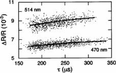
FIGURE 3.7. Comparison of measured normalized pulse heights ( R/R) and pulse widths (τ ) and the predictions of Eqs. (3.4) and (3.5). Each point represents the measured pulse height vs pulse width for the passage of a 470 nm diameter latex colloid (lower group of points) or a 514 nm diameter latex colloid (upper group of points) through a pore of length 0.4 µm and diameter 1.16 µm. For each type of colloid, the correlation between the measured heights and widths of the pulses is a result of the effect of colloids that travel off the pore axis. The measured data agree well with the predictions of Eqs. (3.4) and (3.5) for each colloid size, shown here as the solid lines. [From Ref. 16.]
In Fig. 3.7, we plot the values we measured of the normalized change in electrical resistance R/R vs. τ for pulses produced by two populations of latex colloids: one population with a mean diameter of 470 nm, and one with a mean diameter of 514 nm. The data was taken using a pore that is 9.4 µm in length and 1.16 µm in diameter. For both types of colloids, there is a clear positive and nearly linear correlation between R/R and τ as qualitatively expected from Eqs. 3.4 and 3.5. One interpretation of this positive correlation is that it is due to deviations in the size of individual colloids within each population, since it is clear that relatively larger colloids will both move slower and produce larger pulse amplitudes. The 470 nm diameter colloid population shown in the lower portion of the data plotted in Fig. 3.7 has a standard deviation of 12 nm as measured by the manufacturer. Eq. 3.4 predicts that the expected variation in τ of on-axis particles, due solely to differences in particle size within the population, will be 2%. As seen in Fig. 3.7, the measured values for τ vary by much more than that ( 80%). We thus conclude that the measured variations in τ can be attributed almost entirely to off-axis effects and not to differences in particle size.
Given particle and pore dimensions, we can use Eqs. 3.4 and 3.5 to find the predicted dependence of R on τ due to the off-axis effects. In Fig. 3.7, we plot this result and compare it to the measured data. For both types of colloids, we find good agreement between the predicted dependence and the measurements when α = 6 in Eq. 3.5; this value for α falls well within the range Berge et al. [17] found. The nearly linear measured correlation between
R and τ is then explained by the fact that variations in R (caused by both electrical noise and the intrinsic size distribution of the colloid population) obscure the slight nonlinearity in the predicted dependence. Based on this, we propose that off-axis effects can be effectively removed in the data analysis of a given population by first fitting a line f (τ ) to the plot of R vs. τ , and then calculating an adjusted value Radj for each event of height
R and width τ :
Radj = R − [ f (τ ) − f (τmin)] |
(3.6) |