

Universal Serial Bus Specification Revision 1.1
Chapter 7
Electrical
This chapter describes the electrical specification for the USB. It contains signaling, power distribution, and physical layer specifications.
7.1 Signaling
The signaling specification for the USB is described in the following subsections.
7.1.1 USB Driver Characteristics
The USB uses a differential output driver to drive the USB data signal onto the USB cable. The static output swing of the driver in its low state must be below VOL (max) of 0.3V with a 1.5k load to 3.6V and in its high state must be above the VOH (min) of 2.8V with a 15k load to ground as listed in Table 7-5. Full-speed drivers have more stringent requirements, as described in Section 7.1.1.1. The output swings between the differential high and low state must be well-balanced to minimize signal skew. Slew rate control on the driver is required to minimize the radiated noise and cross talk. The driver’s outputs must support three-state operation to achieve bi-directional half-duplex operation.
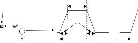
USB devices must be capable of withstanding continuous exposure to the waveforms shown in Figure 7-1 while in any drive state. These waveforms are applied directly into each USB data pin from a voltage source with an output impedance of 39 . The open-circuit voltage of the source shown in Figure 7-1 is based on the expected worst-case overshoot and undershoot.
It is recommended that these DC and AC stresses be used as qualification criteria against which the longterm reliability of each device is evaluated.
Evaluation Setup
|
|
D+ or D- pin |
|
60nS |
|
|
|
|
|
|
|||||
on USB connector |
|
(min) |
|
|
|
|
|
|
|
||||||
|
|
||||||||||||||
|
nearest device |
|
|
|
|
|
|
|
|
|
|||||
|
|
|
|
|
|
|
4.6V |
|
|||||||
|
|
|
|
|
|
|
|
||||||||
|
|
|
|
|
|
|
|
|
|
|
|
|
|
||
|
|
|
|
|
|
|
|
|
|
|
|
||||
|
|
|
|
RSRC |
|
4-20ns |
|||||||||
USB |
|
|
|
|
|||||||||||
|
|
|
|
|
|
|
|
|
|
|
|
||||
|
|
|
|
|
|
|
|
|
|
|
|
|
|
|
|
Device |
|
|
V |
|
|
|
|
|
|
|
|
|
|||
|
|
|
|
|
|
|
|
|
|
|
|||||
|
|
|
|
|
|
|
|
|
|
|
-1.0V |
||||
|
|
|
|
|
|
|
|
|
|
|
|||||
|
|
|
|
|
|
|
|
|
|
|
|
|
|
||
|
|
|
|
|
|
|
|
|
|
|
|
166.7ns |
|||
RSRC = 39 2% |
|
(6MHz) |
|
||
|
|
|
The signal produced by the voltage generator may be |
|
|
distorted when observed at the data pin due to input |
|
|
protection devices possibly incorporated in the USB |
|
|
device. |
|
|
Figure 7-1. Maximum Input Waveforms for USB Signaling
A USB device must be able to withstand a continuous short circuit of D+ and D- to VBUS, GND, other data line, or the cable shield at the connector. The device must not be damaged when presented with a driving signal that provides a duty cycle of 50% transmit and 50% receive. The transmit phase consists of a symmetrical signal that toggles between drive high and drive low. This requirement must be met for max value of VBUS.
107
Universal Serial Bus Specification Revision 1.1
7.1.1.1 Full-speed (12Mb/s) Driver Characteristics
A full-speed USB connection is made through a shielded, twisted pair cable with a characteristic impedance (Z0) of 90 15% and a maximum one-way delay of 26ns. The impedance of each of the drivers (ZDRV) must be between 28 and 44 i.e. within the grey area in Figure 7-3.
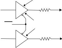
For a CMOS implementation, the driver impedance will typically be realized by a CMOS driver with an impedance significantly less than this resistance with a discrete series resistor making up the balance as shown in Figure 7-2. The series resistor RS is included in the buffer impedance requirement shown in Figure 7-3. In the rest of the chapter, references to the buffer assume a buffer with the series impedance unless stated otherwise.
|
Buffer Output Imped. (ZBUF) |
|
TxD+ |
RS |
|
D+ (28 to 44 Equiv. Imped.) |
||
|
||
OE |
Identical |
|
CMOS |
||
TxD- |
Buffers |
|
D- (28 to 44 Equiv. Imped.) |
||
|
||
|
RS |
|
|
Figure 7-2. Example Full-speed CMOS Driver Circuit |
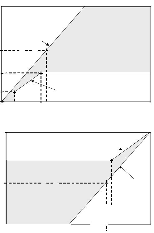
The buffer impedance must be measured for driving high as well as driving low. Figure 7-3 shows the composite V/I characteristics for the full-speed drivers with included series damping resistor (RS). The characteristics are normalized to the steady-state, unloaded output swing of the driver. The normalized driver characteristics are found by dividing the measured voltages and currents by the actual swing of the driver under test. The normalized V/I curve for the driver must fall entirely inside the shaded region. The V/I region is bounded by the minimum driver impedance above and the maximum driver impedance below. The minimum drive region is intersected by a constant current region of |6.1VOH|mA when driving low and -|6.1VOH|mA when driving high. This is the minimum current drive level necessary to ensure that the waveform at the receiver crosses the opposite single-ended switching level on the first reflection.
When testing, the current into or out of the device need not exceed 10.71*VOH mA and the voltage applied to D+/D- need not exceed 0.3*VOH for the drive low case and need not drop below 0.7*VOH for the drive high case.
108
Universal Serial Bus Specification Revision 1.1
|
|
drive low |
|
|
|
IOUT |
|
|
|
|
|
(mA) |
Slope = 1/28 |
|
|
|
|
|
|
|
|
||
10.71 * |VOH| |
Test Limit |
|
|
|
|
6.1 * |VOH| |
|
|
|
|
|
2.32 |
|
|
|
|
|
|
|
|
Slope = 1/44 |
||
0 |
|
|
|
|
|
0 |
0.3V |
0.27*VOH |
0.3*VOH |
VOUT |
VOH |
|
|
|
|
(Volts) |
|
0 |
|
|
|
|
|
drive high
Slope = 1/44 
-6.1*|VOH|
-10.71 * |VOH| |
Test Limit |
|
Slope = 1/28 |
||
|
IOUT
(mA)
|
|
|
|
|
|
|
|
|
|
|
|
|
|
|
|
|
|
|
|
|
|
|
|
|
|
|
|
|
|
|
|
|
|
|
|
|
|
|
|
|
|
|
|
|
|
|
|
|
|
|
|
|
|
|
|
|
|
|
|
|
|
|
0 |
VOUT (Volts) |
0.7*VOH |
|
0.73*VOH |
VOH |
|
|
|
|
|
|||
|
|
|
|
|
|
|
Figure 7-3. Full-speed Buffer V/I Characteristics
109
Universal Serial Bus Specification Revision 1.1
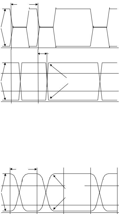
Figure 7-4 shows the full-speed driver signal waveforms.
One Bit
Time
(12Mb/s)
Driver
Signal Pins
VSS
VIH (min)
Receiver
Signal Pins
One-Way
Trip Cable |
Delay |
Signal pins pass |
input spec levels |
after one cable |
delay |
VIL (max)
VSS
Figure 7-4. Full-speed Signal Waveforms
7.1.1.2 Low-speed (1.5Mb/s) Driver Characteristics
A low-speed device must have a captive cable with the Series A connector on the plug end. The combination of the cable and the device must have a single-ended capacitance of no less than 200pF and no more than 450pF on the D+ or D- lines.
The propagation delay (TLSCBL) of a low-speed cable must be less than 18ns. This is to ensure that the reflection occurs during the first half of the signal rise/fall, which allows the cable to be approximated by a lumped capacitance.
VIH (min)
Driver
Signal Pins
VIL (max)
VSS
One Bit |
Time |
(1.5Mb/s) |
Signal pins |
pass output |
spec levels |
with minimal |
reflections and |
ringing |
Figure 7-5. Low-speed Driver Signal Waveforms
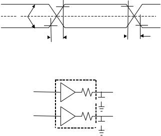
7.1.2 Data Signal Rise and Fall
The output rise time and fall times are measured between 10% and 90% of the signal (Figure 7-6). Rise and fall time requirements apply to differential transitions as well as to transitions between differential and single-ended signaling.
110
Universal Serial Bus Specification Revision 1.1
The rise and fall times for full-speed buffers are measured with the load shown in Figure 7-7. The rise and fall times must be between 4ns and 20ns, and matched to within 10% to minimize RFI emissions and signal skew. The transitions must be monotonic.
The rise and fall times for low-speed buffers are measured with the load shown in Figure 7-8. The capacitive load shown in Figure 7-8 is representative of the worst-case load allowed by the specification. A downstream port is allowed 150pF of input/output capacitance (CIND). A low-speed device (including cable) may have a capacitance of as little as 200pF and as much as 450pF. This gives a range of 200pF to 600pF as the capacitive load that a downstream low-speed buffer might encounter. Upstream buffers on low-speed devices must be designed to drive the capacitance of the attached cable plus an additional 150pF. If a low-speed buffer is designed for an application where the load capacitance is known to fall in a different range, the test load can be adjusted to match the actual application. Low-speed buffers on hosts and hubs that are attached to USB receptacles must be designed for the 200pF to 600pF range. The rise and fall time must be between 75ns and 300ns for any balanced, capacitive test load. In all cases, the edges must be matched to within 20% to minimize RFI emissions and signal skew. The transitions must be monotonic.
For both full-speed and low-speed signaling, the crossover voltage (VCRS) must be between 1.3V and 2.0V.
This specification does not require matching signal swing matching to any greater degree than described above. However, when signaling, it is preferred that the average voltage on the D+ and D- lines should be constant. This means that the amplitude of the signal swing on both D+ and D- should be the same; the low and high going transition should begin at the same time and change at the same rate; and the crossover voltage should be the same when switching to a J or K. Deviations from signal matching will result in common-mode noise that will radiate and affect the ability of devices and systems to pass tests that are mandated by government agencies.
|
Rise Time |
|
|
|
Fall Time |
|||
VCRS |
|
|
|
90% |
90% |
|
||
|
|
|
|
|
|
|||
|
|
|
|
|
|
|
|
|
|
10% |
|
|
10% |
||||
|
|
|
|
|
|
|||
Differential |
|
|
tR |
|
|
|
|
tF |
Data Lines |
|
|
|
|
|
|
||
|
|
|
||||||
Figure 7-6. Data Signal Rise and Fall Time
Full-speed
Buffer
RS
TxD+

 CL
CL
RS
TxD-

 CL
CL
CL = 50pF
Figure 7-7. Full-speed Load
111