

Universal Serial Bus Specification Revision 1.1
should be used on the other end of the cable under test, to convert the signal back to unbalanced from of the correct impedance to match the network analyzer.
6.7.1 Applicable Documents
American National Standard/Electronic Industries Association
ANSI/EIA-364-C (12/94) Electrical Connector/Socket Test Procedures
Including Environmental Classifications
American Standard Test Materials
ASTM-D-4565 |
Physical and Environmental Performance Properties |
|
of Insulation and Jacket for Telecommunication |
|
Wire and Cable, Test Standard Method |
ASTM-D-4566 |
Electrical Performance Properties of Insulation and |
|
Jacket for Telecommunication Wire and Cable, Test |
|
Standard Method |
Underwriters’ Laboratory, Inc. |
|
UL STD-94 |
Test for Flammability of Plastic materials for Parts |
|
in Devices and Appliances |
UL Subject-444 |
Communication Cables |
6.8USB Grounding
The shield must be terminated to the connector plug for completed assemblies. The shield and chassis are bonded together. The user selected grounding scheme for USB devices and cables must be consistent with accepted industry practices and regulatory agency standards for safety and EMI/ESD/RFI.
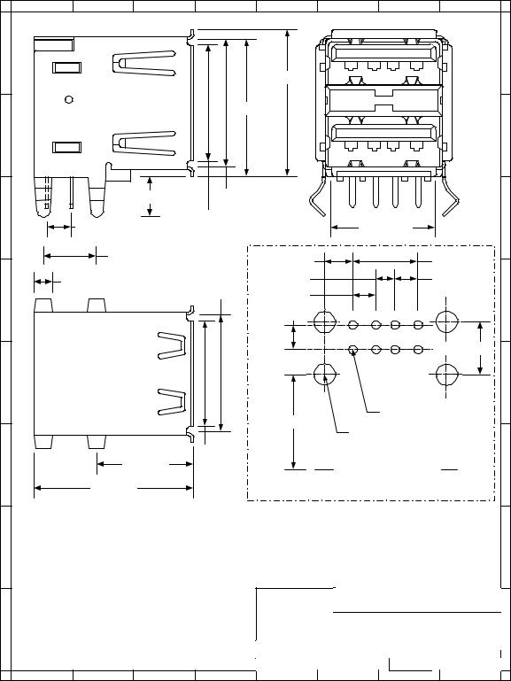
6.9 PCB Reference Drawin gs
The following drawings describe typical receptacle PCB interfaces. This is included for information purposes only.
102

Universal Serial Bus Specification Revision 1.1
8 |
7 |
6 |
5 |
4 |
3 |
2 |
1 |
|
|
|
|
|
|
|||||
H |
|
|
|
|
|
|
|
|
|
H |
|
|
|
|
|
|
|
6.5 REF |
|
16.0 REF |
|
|
|
|
|
|
|
|
|
|
|
|
|
|
13.1 REF |
|
|
|
2.80 + 0.10 |
13.9 REF |
|
||
|
|
|
|
|
|
|
|
|
||
|
|
|
|
2.0 REF |
|
|
|
|
|
|
G |
|
|
|
|
|
|
|
|
|
G |
|
14.3 |
REF |
|
|
|
|
10.3 REF |
|
|
|
|
|
|
|
|
|
|
|
|
||
|
|
|
|
|
|
|
3.8 REF |
|
|
|
F |
|
15.0 REF |
|
|
|
|
|
|
F |
|
|
|
|
|
|
7.6 REF |
6.00 + 0.10 |
|
|
||
|
|
|
|
|
|
|
|
|
||
|
|
12.5 + 0.10 |
|
R 0.64 + 0.13 Typical (2) |
|
|
|
|||
|
|
11.1 + 0.10 |
1.84 + 0.05 |
|
|
|
|
|||
|
|
|
|
|
|
|
|
|||
E |
|
1 |
2 3 4 |
|
|
5.12 + 0.10 |
|
|
E |
|
|
9.0 REF |
|
|
|
|
|
|
|||
|
|
|
|
|
|
|
|
|
||
|
10.7 REF |
|
|
|
|
|
|
|
|
|
|
|
|
|
|
2.56 + 0.05 |
|
|
|
|
|
|
|
|
|
|
Thermoplastic Insulator UL 94-V0 |
|
|
|||
D |
|
2.50 + 0.05 |
|
2.50 + 0.05 |
1.0 + 0.05 Wide - Selectively Plated Contact (4) |
D |
||||
|
|
|
|
|
|
|
||||
|
2.00 + 0.05 |
|
|
|
|
|
|
|
|
|
|
Ø 0.92 + |
0.10 (4) |
|
|
NOTES: |
|
|
|
|
|
|
7.00 + 0.10 |
|
|
1. |
Critical Dimensions are TOLERANCED |
|
||||
C |
2.00 + 0.10 |
|
|
|
and should not be deviated. |
|
C |
|||
|
|
|
|
|
|
|||||
|
|
|
|
|
2. |
Dimensions that are labeled |
REF are |
|
||
|
|
|
|
|
|
typical dimensions and may vary from |
|
|||
|
2.71 + 0.10 |
|
|
|
manufacturer to manufacturer. |
|
|
|||
|
|
|
|
|
|
|
|
|
||
B |
|
13.14 + 0.10 |
|
3. |
All dimensions are in millimeters (m m ) unless B |
|||||
|
|
|
|
|
|
otherwise noted. |
|
|
|
|
|
|
Ø 2.30 + |
0.10 (2) |
|
|
|
|
|
|
|
|
Printed Circuit Board (PCB) Layout |
|
|
|
Single Pin-Type |
|
||||
|
|
|
|
|
|
|
|
|
||
A |
|
|
|
|
|
|
|
Series "A" Receptacle |
||
|
|
|
|
|
|
|
|
|
A |
|
|
|
|
|
|
|
|
SIZE |
DATE |
DRAWING NUMBER |
REV |
|
|
|
|
|
|
|
A |
2/98 |
N/A |
C |
|
|
|
|
|
|
|
SCALE: N/A |
SHEET |
1 of 1 |
|
|
8 |
7 |
6 |
|
5 |
4 |
3 |
|
2 |
1 |
Figure 6-12. Single Pin-Type Series "A" Receptacle
103
Universal Serial Bus Specification Revision 1.1
8 |
7 |
6 |
5 |
4 |
3 |
|
2 |
1 |
H |
|
|
|
|
1 |
2 |
3 |
4 |
|
|
|
|
|
|
|
H |
|
|
|
|
|
15.60 REF |
|
|
|
|
|
|
|
|
14.70 ± 0.10 |
|
|
|
|
|
|
|
|
|
1 |
2 |
3 |
4 |
G |
|
|
|
|
|
|
|
G |
|
|
3.70 REF |
13.78 + 0.10 |
|
|
|
|
||
F |
|
2.62 ± 0.05 |
|
12.30 REF |
|
|
|
|
F |
|
|
|
|
11.01 ± 0.10 |
|||||
|
|
|
|
|
|
||||
|
|
5.70 REF |
|
|
3.07 ± 0.10 (2) |
|
|
7.00 ± 0.10 |
|
|
|
|
|
|
|
|
|||
|
|
2.00 REF |
|
12.50 + 0.10 |
2.00 ± 0.10 |
|
|
2.50 ± 0.10 |
|
|
|
|
|
2.50 ± 0.10 |
|
|
|
|
|
|
|
|
|
|
|
|
|
|
|
E |
|
|
|
|
2.62 ± 0.05 |
|
|
|
E |
|
|
|
|
|
|
|
|
|
|
|
|
|
|
|
|
|
|
5.68 ± 0.10 |
|
D |
|
|
|
|
|
|
|
|
D |
|
|
|
|
|
10.28 ± 0.20 |
|
|
Ø 0.92 ± 0.10 (8) |
|
|
|
|
|
|
|
|
|
|
|
|
|
|
|
|
|
Ø 2.3 ± 0.10 (4) |
|
||
|
|
|
|
11.10 REF |
|
|
|
|
|
C |
|
10.30 REF |
|
|
Connector Front Edge |
C |
|||
|
|
|
|
|
|||||
|
|
16.95 REF |
|
|
Printed Circuit Board (PCB) Layout |
|
|||
|
NOTES: |
|
|
|
|
|
|
|
|
B |
1. Critical Dimensions are TOLERANCED |
|
|
|
|
B |
|||
and should not be deviated. |
|
|
|
|
|
||||
|
|
|
|||||||
|
|
|
|
|
|||||
|
2. Dimensions that are labeled REF are |
|
|
|
|
|
|||
|
typical dimensions and may vary from |
|
|
Dual Pin-Type |
|
||||
|
manufacturer to manufacturer. |
|
Series "A" Receptacle |
||||||
A |
|
|
|
|
|
||||
3. All dimensions are in millimeters ( m m ) |
|
|
|
|
A |
||||
|
|
SIZE |
DATE |
DRAWING NUMBER |
REV |
||||
|
unless otherwise noted. |
|
|
|
A |
2/98 |
N/A |
C |
|
|
|
|
|
|
|
SCALE: |
N/A |
SHEET |
1 of 1 |
|
8 |
7 |
6 |
5 |
4 |
3 |
|
2 |
1 |
Figure 6-13. Dual Pin-Type Series "A" Receptacle
104
Universal Serial Bus Specification Revision 1.1
8 |
7 |
6 |
5 |
4 |
3 |
2 |
1 |
|
1.0 + 0.05 Wide - Selectively Plated Contacts (4) .... |
|
|
H |
Thermoplastic Insulator UL 94-V0 .... |
|
H |
|
|
|
|
|
7.78 + 0.10 |
2 |
1 |
|
|
|
|
G |
11.50 REF |
|
G |
|
5.60 + 0.10 |
3 |
4 |
|
|
|
|
|
|
|
|
|
|
|
|
|
|
|
|
|
|
|
|
|
|
|
|
|
|
|
|
|
|
|
|
|
|
|
|
|
|
|
|
|
|
|
|
|
|
|
|
|
|
|
|
|
|
|
|
|
|
|
|
|
|
|
|
|
|
|
|
|
|
|
|
|
|
|
|
|
|
|
|
|
|
|
|
|
|
|
|
|
|
|
|
|
|
|
|
|
|
|
|
|
|
|
|
|
|
|
|
|
|
|
|
|
|
|
|
|
|
|
|
|
|
|
|
|
|
|
|
|
|
|
|
|
|
|
|
|
|
|
|
|
|
|
|
|
|
|
|
|
|
|
|
|
|
|
|
|
|
|
|
|
|
|
|
|
|
|
|
|
|
|
|
|
|
|
|
|
|
|
|
|
|
|
|
|
|
|
|
|
|
|
|
|
|
|
|
|
|
|
|
|
|
|
|
|
|
|
|
|
|
|
|
|
|
|
|
|
|
|
|
|
|
|
|
|
|
|
|
|
|
|
|
|
|
|
|
|
|
|
|
|
|
|
|
|
|
|
|
|
|
|
|
|
|
|
|
|
|
|
|
|
|
|
|
|
|
|
|
|
|
|
|
|
|
|
|
|
|
|
|
|
|
|
|
|
|
|
|
|
|
|
|
|
|
|
|
|
|
|
|
|
|
|
|
|
|
|
|
|
|
|
|
|
|
|
|
|
|
|
|
|
|
|
|
|
|
|
|
|
|
|
|
|
|
|
|
|
|
|
|
|
|
|
|
|
|
|
|
|
|
|
|
|
|
|
|
|
|
|
|
|
|
|
|
F |
|
|
|
|
|
|
|
|
|
|
|
|
|
|
|
|
|
|
|
|
|
|
|
|
|
|
|
|
|
|
|
|
|
|
|
|
|
|
|
|
|
|
|
|
|
|
|
|
|
|
|
|
|
|
|
|
|
|
|
|
|
|
|
|
|
|
|
|
|
|
|
|
|
|
|
|
|
|
F |
|||||||||||
|
|
|
|
|
|
|
|
|
|
|
|
|
|
|
|
|
|
|
|
|
|
|
|
|
|
|
|
|
|
|
|
|
|
|
|
|
|
|
|
|
|
|
|
|
|
|
|
|
|
|
|
|
|
|
|
|
|
|
|
|
|
|
|
|
|
|
|
|
|
|
|
|
|
|
||||||||||||||||
|
|
|
|
|
|
|
|
|
|
|
|
|
|
|
|
|
|
|
|
|
|
|
|
|
|
|
|
|
|
|
|
|
|
|
|
|
|
|
|
|
|
|
|
|
|
|
|
|
|
|
|
|
|
|
|
|
|
|
|
|
|
|
|
|
|
|
|
|
|
|
|
|
|
|
||||||||||||||||
|
|
|
|
|
|
|
|
|
|
|
|
|
|
|
|
|
|
|
|
|
|
|
|
|
|
|
|
|
|
|
|
|
|
|
|
|
|
|
|
|
|
|
|
|
|
|
|
|
|
|
|
|
|
|
|
|
|
|
|
|
|
|
|
|
|
|
|
|
|
|
|
|
|
|
||||||||||||||||
|
|
|
|
|
|
|
|
|
|
|
|
|
|
|
|
|
|
|
|
|
|
|
|
|
|
|
|
|
|
|
|
|
|
|
|
|
|
|
|
|
|
|
|
|
|
|
|
|
|
|
|
|
|
|
|
|
|
|
|
|
|
|
|
|
|
|
|
|
|
|
|
|
|
|
||||||||||||||||
|
|
|
|
2.71 + 0.10 |
|
|
|
|
|
|
|
|
|
|
3.01 + 0.10 |
|
|
|
|
|
|
|
3.50 REF |
|
|
|
|
|
|
|
|
|
|
|
|
|
|
|
|
|
|
|
|
|
|
|
|
|
|
|
|
|
|
|
|
|
|
|
|
|
|
|
|
|
2.50 + 0.10 |
|
|
|||||||||||||||||||||||
|
|
|
|
|
|
|
|
|
|
|
|
|
|
|
|
|
|
|
|
|
|
|
|
|
|
|
|
|
|
|
|
|
|
|
|
|
|
|
|
|
|
|
|
|
|
|
|
|
|
|
|
|
|
|
|
|
|
|
|
|
|
|
|
|
|
|
|
|
|
|
|
|
|
|
|
|
|
|
|
|
|
|||||||||
|
|
|
|
|
|
|
|
|
|
|
|
|
|
|
|
|
|
|
|
|
|
|
|
|
|
|
|
|
|
|
|
|
|
|
|
|
|
|
|
|
|
|
|
|
|
|
|
|
|
|
|
|
|
|
|
|
|
|
|
|
|
|
|
|
|
|
|
|
||||||||||||||||||||||
|
|
|
|
|
|
|
|
|
|
|
|
|
|
|
|
|
|
|
|
|
|
|
|
|
|
|
|
|
|
|
|
|
|
|
|
|
|
|
|
|
|
|
|
|
|
|
|
|
|
|
|
|
|
|
|
|
|
|
|
|
|
|
|
|
|
|
|
|
|
|
|
|
|
|
|
|
|
|
|
|
|
|
||||||||
|
|
|
|
|
|
|
|
|
|
|
|
|
|
|
|
|
|
|
|
|
|
|
|
|
|
|
|
|
|
|
|
|
|
|
|
|
|
|
|
|
||||||||||||||||||||||||||||||||||||||||||||||||||
|
|
|
|
|
|
|
|
|
|
|
|
|
|
|
|
|
|
|
|
|
|
|
|
|
|
|
|
|
|
|
|
|
|
|
|
|
|
|
|
|
|
|
|
|
|
|
|
|
|
|
|
|
|
|
8.45 + 0.10 |
|
|
|
|
|
|
|
|
|
|
|
|
|
|
|
|
|
|
|||||||||||||||||
|
|
|
|
|
|
|
|
|
|
|
|
|
|
|
|
|
|
|
|
|
|
|
|
|
|
|
|
|
|
|
|
|
|
|
|
|
|
|
|
|
|
|
|
|
|
|
|
|
|
|
|
|
|
|
|
|
|
|
|
|
|
|
|
|
|
|
|
|
|
|
|
|
||||||||||||||||||
|
|
|
|
|
|
|
|
|
|
|
|
|
|
|
|
|
|
|
|
|
|
|
|
|
|
|
|
|
|
|
|
|
|
|
|
|
|
|
|
|
|
|
|
|
|
|
||||||||||||||||||||||||||||||||||||||||||||
|
|
|
|
|
|
|
|
|
|
|
|
|
|
|
|
|
|
|
|
|
|
|
|
|
|
|
|
|
|
|
|
|
|
|
|
|
|
|
|
|
|
|
|
|
|
|
|
|
|
|
|
|
|
|
|
|
|
|
|
|
|
|
|
|
|
|
|
|
|
|
|
|||||||||||||||||||
|
|
|
|
|
|
|
|
|
|
|
|
|
|
|
|
2.00 + 0.10 |
|
|
|
|
|
|
|
|
|
|
|
|
|
|
|
|
|
|
|
|
|
|
|
|
|
|
|
|
|
|
|
|
|
|
|
|
|
|
|
|
|
|
|
|
|
|
|
|
|
|
|
|
|
|||||||||||||||||||||
|
|
|
|
|
|
|
|
|
|
|
|
|
|
|
|
|
|
|
|
|
|
|
|
|
|
|
|
|
|
|
|
|
|
|
|
|
|
|
|
|
|
|
|
|
|
|
|
|
|
|
|
|
|
|
|
|
|
|
|
|
|
|
|
|
|
|
|
|
|
|
|
|
|
|
|
|
|
|
|
|
|
|
|
|
|
|||||
|
|
|
|
|
|
|
|
|
|
|
|
|
|
|
|
|
|
|
|
|
|
|
|
|
|
|
|
|
|
|
|
|
|
|
|
|
|
|
|
|
|
|
|
|
|
|
|
|
|
|
|
|
|
|
|
|
|
|
|
|
|
|
|
|
|
|
|
|
|
|
|
|
|
|
|
|
|
|
|
|
|
|
|
|
||||||
E |
|
|
4.71 + 0.10 |
|
|
|
|
|
|
|
|
|
|
|
|
|
|
|
|
|
|
|
|
|
|
|
|
|
|
|
|
|
|
|
|
|
|
|
|
|
|
|
|
|
|
|
|
|
|
|
|
|
|
|
|
|
|
|
|
|
|
|
|
|
|
|
|
|
|
|
|
|
|
|
|
|
|
|
|
|
|
|
|
E |
||||||
|
|
|
|
|
|
|
|
|
|
|
|
|
|
|
|
|
|
|
|
|
|
|
|
|
|
|
|
|
|
|
|
|
|
|
|
|
|
|
|
|
|
|
|
|
|
|
|
|
|
|
|
|
|
|
|
|
|
|
|
|
|
|
|
|
|
|
|
|
|
|
|
|
|
|
|
|
|
|
|
|
|
|
|
|
|
|
||||
|
|
|
|
|
|
|
|
|
|
|
|
|
|
|
|
|
|
|
|
|
|
|
|
|
|
|
|
|
|
|
|
|
|
|
|
|
|
|
|
|
|
|
|
|
|
|
|
|
|
|
|
|
|
|
|
|
|
|
|
|
|
|
|
|
|
|
|
|
|
|
|
|
|
|
|
|
|
|
|
|
|
|
|
|
|
|
||||
|
|
|
|
|
|
|
|
|
|
|
|
|
|
|
|
|
|
|
|
|
|
|
|
|
|
|
|
|
|
|
|
|
|
|
|
|
|
|
|
|
|
|
|
|
|
|
|
|
|
|
|
|
|
|
|
|
|
|
|
|
|
|
|
|
|
|
|
|
|
|
|
|
|
|
|
|
|
|
|
|
|
|
|
|
||||||
|
|
|
|
|
|
|
|
|
|
|
|
|
|
|
|
|
|
|
|
|
|
|
|
|
|
|
|
|
|
|
|
|
|
|
|
|
|
|
|
|
|
|
|
|
|
|
|
|
|
|
|
|
|
|
|
|
|
|
|
|
|
|
|
|
|
|
|
|
|
|
|
|
|
|
|
|
|
|
|
|
|
|
|
|
|
|
|
|||
|
|
|
|
|
|
|
|
|
|
|
|
|
|
|
|
|
|
|
|
|
|
|
|
|
|
|
|
|
|
|
|
|
|
|
|
|
|
|
|
|
|
|
|
|
|
|
|
|
|
|
|
|
|
|
|
|
|
|
|
|
|
|
|
|
|
|
|
|
|
|
|
|
|
|
|
|
|
|||||||||||||
|
|
|
|
|
|
|
|
|
|
|
|
|
|
|
|
|
|
|
|
|
|
|
|
|
|
|
|
|
|
|
|
|
|
|
|
|
|
|
|
|
|
|
|
|
|
|
|
|
|
|
|
|
|
|
|
|
|
|
|
|
|
|
|
|
|
|
|
|
|
|
|
|
|
|
|
|
|
|||||||||||||
|
|
|
|
|
|
|
|
|
|
|
|
|
|
|
|
|
|
|
|
|
|
|
|
|
|
|
|
|
|
|
|
|
|
|
|
|
|
|
|
|
|
|
|
|
|
|
|
12.04 + 0.10 |
|
|
|
|
|
|
|
|
|
|
|
|
|
|
|
|
|
|||||||||||||||||||||||||
|
|
|
|
|
|
|
|
|
|
|
|
|
|
|
|
|
|
|
|
|
|
|
|
|
|
|
|
|
|
|
|
|
|
|
|
|
|
|
|
|
|
|
|
|
|
|
|
|
|
|
|
|
|
|
|
|
|
|
|
|
|
|
|
|
|
|
|
|
|
|
|
|
|
|
|
|
|
|
|
|
|
|
|
|
|
|
|
|
|
|
|
|
|
|
|
|
|
|
|
|
|
|
|
|
|
|
|
|
|
|
|
|
|
|
2.50 |
+ 0.10 |
|
|
|
|
|
|
|
|
|
|
|
|
|
|
|
|
|
|
|
|
|
|
|
|
|
|
|
|
|
|
|
|
|
|
|
|
|
|
|
|
|
|
|
|
|
|
|
|
|
|
|
|
|
||||||||||||
|
|
|
|
|
|
|
|
|
|
|
|
|
|
|
|
|
|
|
|
|
|
|
|
|
|
|
|
|
|
|
|
|
|
|
|
|
|
|
|
|
|
|
|
|
|
|
|
|
|
|
|
|
|
|
|
|
|
|
|
|
|
|
|
|
|
|
|
|
|
|
|
|
|
|
||||||||||||||||
|
|
|
|
|
|
|
|
|
|
|
|
|
|
|
|
|
|
|
|
|
|
|
|
|
|
|
|
|
|
|
|
|
|
|
|
|
|
|
|
|
|
|
|
|
|
|
|
|
|
|
|
|
|
|
|
|
|
|
|
|
|
|
|
|
|
|
|
|
|
|
|
|
|
|
|
|||||||||||||||
|
|
|
|
|
|
|
|
|
|
|
|
|
|
|
|
|
|
|
|
|
|
|
|
4.77 |
+ 0.10 |
|
|
|
|
|
|
|
|
|
|
|
|
|
|
|
|
|
|
|
|
|
|
|
|
|
|
|
|
|
|
|
|
|
|
|
|
|
|
|
|
|
|
|
|
|
|
|
|
|
|
|
|
|
||||||||||||
|
|
|
|
|
|
|
|
|
|
|
|
|
|
|
|
12.00 REF |
|
|
|
|
|
|
|
|
|
|
|
|
|
|
|
|
|
|
|
|
|
|
|
|
|
|
|
|
|
|
|
|
|
|
|
|
|
|
|
|
|
|
|
|
|
|
|
|
|
|
|
|
||||||||||||||||||||||
|
|
|
|
|
|
|
|
|
|
|
|
|
|
|
|
|
|
|
|
|
|
|
|
|
|
|
|
|
|
|
|
|
|
|
|
|
|
|
|
|
|
|
|
|
|
|
|
|
|
|
|
|
|
|
|
|
|
|
|
|
|
|
|
|
|
|
|
|
|
|
|
|||||||||||||||||||
|
|
|
|
|
|
|
|
|
|
|
|
|
|
|
|
|
|
|
|
|
|
|
|
|
|
|
|
|
|
|
|
|
|
|
|
|
|
|
|
|
|
|
|
|
|
|
|
|
|
|
|
|
|
|
|
|
|
|
|
|
|
|
|
|
|
|
|
|
|
|
|
|
|
|
|
|
|
|
|
|
|
|
|
|
|
|
||||
D |
|
|
|
|
|
|
|
|
|
|
|
|
|
|
|
|
|
|
|
|
|
|
2.00 |
+ 0.10 |
|
|
|
|
|
|
|
|
|
|
|
|
|
|
|
|
|
|
|
|
|
|
|
|
|
|
|
|
|
|
|
|
|
|
|
|
|
|
|
|
|
|
|
|
|
|
|
|
|
|
|
|
D |
|||||||||||||
|
|
|
|
|
|
|
|
|
|
|
|
|
|
|
|
|
|
|
|
|
|
|
|
|
|
|
|
|
|
|
|
|
|
|
|
|
|
|
|
|
|
|
|
|
|
|
|
|
|
|
|
|
|
|
|
|
|
|
|
|
|
|
|
|
|
|
|
|
|
|
|
|
|
|
|
|
|
|
|
|
|
|
|
|
|
|
|
|||
|
|
|
|
|
|
|
|
|
|
|
|
|
|
|
|
|
|
|
|
|
|
|
|
|
|
|
|
|
|
|
|
|
|
|
|
|
|
|
|
|
|
|
|
|
|
|
|
|
|
|
|
|
|
|
|
|
|
|
|
|
|
|
|
|
|
|
|
|
|
|
|
|
|
|
|
|
|
|
|
|
|
|
|
|
|
|
|
|||
|
|
|
|
|
|
|
|
|
|
|
|
|
|
|
|
|
|
|
|
|
|
|
|
|
|
|
|
|
|
|
|
|
|
|
|
|
|
|
|
|
|
|
|
|
|
|
|
|
|
|
|
|
|
|
|
|
|
|
|
|
|
|
|
|
|
|
|
|
|
|
|
|
|
|
|
|
|
|
|
|
|
|
|
|
|
|
|
|
|
|
|
|
|
|
|
|
|
|
|
|
|
|
|
|
|
|
|
|
|
|
|
|
|
|
|
|
|
|
|
|
|
|
|
|
|
|
|
|
|
|
|
|
|
|
|
|
|
|
|
|
|
|
|
|
|
|
|
|
|
|
|
|
|
|
|
|
|
|
|
|
|
|
|
|
|
|
|
|
|
|
|
|
|
|
|
|
|
|
|
|
|
C |
|
|
|
10.30 REF |
|
|
|
|
|
|
|
|
2.71 + 0.10 |
|
|
|
|
|
|
|
|
|
|
|
|
|
|
|
|
|
|
|
|
|
|
|
|
|
|
|
|
|
|
|
|
|
|
|
|
|
|
C |
|||||
|
|
|
|
|
|
|
|
|
|
|
|
|
|
|
|
|
|
|
|
|
|
|
|
|
|
|
|
|
|
|
|
|
|
|
|
|
|
|
|
|
|
|
|
|
|
|
|
|
|
|
|
|
|
|
|||
|
|
|
|
|
|
|
|
|
|
|
|
|
|
|
|
|
|
|
|
|
|
|
|
|
|
|
|
|
|
|
|
|
|
|
|
|
|
|
|
|
|
|
|
|
|
|
|
|
|
|
|
|
|
|
|||
|
|
|
|
|
|
|
|
|
|
|
|
|
|
|
|
|
|
|
|
|
|
|
|
|
|
|
|
|
|
|
|
|
|
|
|
|
|
|
|
|
|
|
|
|
|
|
|
|
|
|
|
|
|
|
|||
|
|
|
|
16.00 REF |
|
|
|
|
|
|
|
|
|
|
|
|
|
|
|
|
|
|
|
|
|
|
|
|
|
|
|
|
|
|
|
|
|
|
|
|
|
|
|
|
|
|
|
|
|
|
|
|
|||||
|
|
|
|
|
|
|
|
|
|
|
|
|
|
|
|
|
|
|
|
|
|
|
|
|
|
|
|
|
|
|
|
|
|
|
|
|
|
|
|
|
|
|
|
|
|
|
|
|
|
|
|
|
|
|
|
|
|
|
NOTES: |
|
|
|
|
|
|
|
|
|
|
|
|
|
Ø 0.92 + |
0.1 |
(4) |
|
|
|
|
|
|
|
|
|
|
|
|
|
|
|
|
|
|
|
|
|
|
|
|
|
|
|
|
|
|
||||||||||
|
|
|
|
|
|
|
|
|
|
|
|
|
|
|
|
|
|
|
|
|
|
|
|
|
|
|
|
|
|
|
|
|
|
|
|
|
|
|
|
|
|
|
|
||||||||||||||
|
|
|
|
|
|
|
|
|
|
|
|
|
|
|
|
|
|
|
|
|
|
|
|
|
|
|
|
|
|
|
|
|
|
|
|
|
|
|
|
|
|
|
|
|
|
|
|
|
|
|
|
|
|
|
|||
|
|
|
|
|
|
|
|
|
|
|
|
|
|
|
|
|
|
|
|
|
|
|
|
|
|
|
|
|
|
|
|
|
|
|
|
|
|
|
|
|
|
|
|
|
|
|
|
|
|
|
|
|
|
|
|||
|
|
|
|
|
|
|
|
|
|
|
|
|
|
|
|
|
|
|
|
|
|
|
|
|
|
|
|
|
|
|
|
|
|
|
|
|
|
|
|
||||||||||||||||||
|
|
|
|
|
|
|
|
|
|
|
|
|
|
|
|
|
|
Ø 2.30 + 0.1 |
(2) |
|
|
|
|
|
|
|
|
|
|
|
|
|
|
|
|
|
|
|
|||||||||||||||||||
|
|
|
|
|
|
|
|
|
|
|
|
|
|
|
|
|
|
|
|
|
|
|
|
|
|
|
|
|
|
|
|
|
|
|
|
|
|
|
|
|
|
|
|
|
|
|
|
|
|
|
|
|
|
|
|
|
|
1. |
Critical Dimensions are TOLERANCED |
|
|
Printed Circuit Board (PCB) Layout |
|
|
|
|
|
|
|
|
|||||||||||||||||||||||||||||||||||||||||||||
|
|
|
|
|
|
|
|
|
|
||||||||||||||||||||||||||||||||||||||||||||||||
B |
and should not be deviated. |
|
|
|
|
|
|
|
|
|
|
|
|
|
|
|
|
|
|
|
|
|
|
|
|
|
|
|
|
|
|
|
|
|
|
|
|
|
|
|
|
|
|
|
|
|
|
B |
|||||||||
|
|
|
|
|
|
|
|
|
|
|
|
|
|
|
|
|
|
|
|
|
|
|
|
|
|
|
|
|
|
|
|
|
|
|
|
|
|
|
|
|
|
|
|
|
|
||||||||||||
2. |
Dimensions that are labeled |
REF are |
|
||||||||||||||||||||||||||||||||||||||||||||||||||||||
|
|
typical dimensions and may vary from |
|
|
|
|
|
|
|
|
|
|
|
|
|
|
|
|
|
|
|
|
|
|
|
|
|
|
|
|
|
|
|
|
|
|
|
|
|
|
|
|
|
|
|
|
|||||||||||
|
|
|
|
|
|
|
|
|
|
|
|
|
|
|
|
|
|
|
|
Single Pin-Type |
|
|
|
|
|
|
|
|
|||||||||||||||||||||||||||||
|
|
manufacturer to manufacturer. |
|
|
|
|
|
|
|
|
|
|
|
|
|
|
|
|
|
|
|
|
|
|
|
|
|
|
|
|
|
||||||||||||||||||||||||||
|
|
|
|
|
|
|
|
|
|
|
|
|
|
|
|
|
|
|
|
|
|
|
|
|
|
|
|
|
|
|
|
|
|
|
|
|
|
|
|
|
|
|
|
|
|
|
|
|
|||||||||
|
|
|
|
|
|
|
|
|
|
|
|
|
|
|
|
|
|
|
|
|
|
|
|
|
|
|
|
|
|
|
|
|
|
|
|
|
|
|
|
|
|
|
|
|
|
|
|
|
|
|
|
|
|
||||
A 3. |
All dimensions are in millimeters ( m m ) |
|
|
|
|
|
|
|
|
|
|
|
Series "B" Receptacle |
|
|||||||||||||||||||||||||||||||||||||||||||
|
|
|
|
|
|
|
|
|
|
|
|
|
|
|
|
|
|
|
|
|
|
|
|
|
|
|
|
|
|
|
|
|
|
|
|
|
|
|
|
|
|
|
A |
||||||||||||||
|
|
unless otherwise noted. |
|
|
|
|
|
|
|
|
|
|
|
|
|
|
|
|
|
|
|
|
|
|
|
|
|
|
|
|
|
|
|
|
|
|
|
|
|
|
|
|
|
|
|
|
|
|
|
||||||||
|
|
|
|
|
|
|
|
|
|
|
|
|
SIZE |
|
|
DATE |
|
|
|
DRAWING NUMBER |
|
|
|
|
REV |
|
|||||||||||||||||||||||||||||||
|
|
|
|
|
|
|
|
|
|
|
|
|
|
|
|
|
|
|
|
|
|
A |
|
2/98 |
|
|
|
|
|
|
|
|
|
N/A |
|
|
|
|
C |
|
|||||||||||||||||
|
|
|
|
|
|
|
|
|
|
|
|
|
|
|
|
|
|
|
|
|
SCALE: N/A |
|
|
|
|
|
|
|
|
|
|
SHEET |
|
1 of 1 |
|
|
|||||||||||||||||||||
|
|
8 |
|
7 |
|
|
|
6 |
|
5 |
4 |
|
|
|
3 |
|
|
|
|
|
|
|
|
|
|
|
2 |
|
|
|
|
|
|
|
|
|
|
1 |
|
|
|
|
|
||||||||||||||
Figure 6-14. Single Pin-Type Series "B" Receptacle
105
Universal Serial Bus Specification Revision 1.1
106