

Biomolecular Sensing Processing and Analysis - Rashid Bashir and Steve Wereley
.pdf350 |
D. FOURGUETTE, E. ARIK, AND D. WILSON |
17.2. CHALLENGES ASSOCIATED WITH OPTICAL DIAGNOSTICS IN MICROFLUIDICS
Optical diagnostics for measurements in microfluidics present inherent challenges [7]. The most challenging aspect for optical diagnostics is the spatial resolution required to obtain meaningful results. The typical wall dimension of a microchannel is on the order of 100 micrometers in diameter, which is comparable to a typical optical probe volume dimension of a laser Doppler velocimeter.
Most optical diagnostics techniques require the presence of scatterers (particles, emulsions, or cells) in the flow to scatter the incident light. Most microfluidics applications do not allow seeding the flow with particles and prefer to rely on the presence of natural scatterers such as cell or emulsions to scatter the light. Unfortunately, the index of refraction of these scatterers is very close to that of the surrounding fluid, thus generating a weak scattered light intensity. In addition, microchannel walls often cause a lensing effect that distorts the incident and scattered light path. This path distortion, often combined with a complex optical access, causes an additional reduction in the signal-to-noise ratio of the measurements.
17.3. ENABLING TECHNOLOGY FOR MICROSENSORS: COMPUTER GENERATED HOLOGRAM DIFFRACTIVE OPTICAL ELEMENTS
The enabling optical elements in these microsensors are the diffractive optical elements (DOEs) that produce the desired optical pattern within such small space. The DOE takes the form of a shallow surface relief pattern that is etched into a transparent substrate. The surface relief pattern is designed to produce phase variation in the laser beam such that the light will form an interference pattern that approximates the desired image. DOEs of this type are frequently referred to as computer-generated holograms (CGHs).
A CGH can be designed using the iterative Fourier transform (IFT) algorithm, also known as the Gerchberg-Saxton algorithm [9]. This algorithm utilizes the well-known Fourier transform relationship between the near field (just past the DOE) and the far field (focal plane of DOE). For high efficiency and ease of fabrication, it is best if the DOE implements a phase-only transmission function, i.e. no spatial magnitude variation is required. This constraint makes it impossible to simply inverse the Fourier transform of the desired far-field image to find the near field (and hence the DOE function) because the inverse transform will generate magnitude variation as well as phase in the near field. The IFT design algorithm overcomes this problem by iterating between the near and far field planes many times, constraining the far-field intensity to the desired pattern and constraining the near field to have phase-only variation. After a sufficient number of iterations, the far field intensity approximates the desired image and the CGH is phase only. Over the last two decades, CGH design methodology had been advanced by a wide-variety of contributions [18].
Being able to perform the design is only the first step in realizing the required DOE for a MOEMS sensor. While there are a variety of techniques for fabricating DOEs [18], the sensors being described here generally require high numerical aperture (low f/#) optics that have micron-scale Fresnel zone spacing. Furthermore, the DOEs must be fabricated with
OPTICAL MEMS-BASED SENSOR DEVELOPMENT WITH APPLICATIONS TO MICROFLUIDICS 351
‘blazed’ analog-relief sawtooth groove shapes to have high diffraction efficiency for measuring the weakly scattering particles. Hence the DOEs must be fabricated using sub-micron features. Such high-efficiency analog-depth DOEs are fabricated at NASA’s Jet Propulsion Laboratory using direct-write electron beam lithography [12, 13, 19, 22]. The DOE surface relief profiles are fabricated in a thin film of E-beam resist (PMGI, polymethylglutarimide, or PMMA, polymethylmethacrylate) that is spin-coated on a fused silica or other substrate to a thickness of approximately two microns. The electron-beam (100 or 50 kV accelerating voltage) breaks bonds in the resist making it more soluble to a development solution. Analog depth control is achieved by varying the E-beam dose (constant current, variable dwell time) in proportion to the desired depth. During pattern preparation, special deconvolution techniques are used to compensate the DOE depth profile for the E-beam proximity effect (backscattered dose) and the non-linear depth vs. dose response of the resist. After exposure, the optic is developed using an iterative procedure in which we measure the depth after each step until the desired depth is achieved. This procedure yields DOEs with depth profiles that are typically accurate to better than 5–10% (λ/20–λ/10) and have diffraction efficiencies in the range 80–90%. Generally the PMGI resist is durable enough for most applications, but if needed, techniques exist to transfer etch the E-beam resist profile into the more durable quartz substrate. If high volume fabrication is desired, a variety of replication techniques have been demonstrated [18].
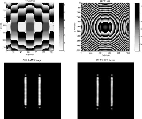
DOEs are capable of shaping light into a wide range of geometries. For example, a DOE was designed and fabricated to shape light into two elongated light spots. This DOE was used in the fabrication of a time-of-flight velocimeter described in Section 17.5.1 [21]. The design was accomplished in two steps. First, the beam-shaping computer-generated hologram (CGH) phase function shown in Fig. 17.1(a) was designed using a variation of the soft-operator IFT algorithm [10] assuming a plane-wave input field and an image at infinity. Second, a commercial ray-tracing program was used to design a lens phase function to focus the light from a single-mode fiber to an image plane at a desired distance beyond the DOE. The lens phase function was optimized to correct for the aberrations introduced by focusing through the substrate. Figure 17.1(b) shows the DOE depth after the lens phase function has been added to the beam-shaping CGH phase function. After E-beam fabrication in PMGI resist on a quartz substrate, the DOE was illuminated with the single-mode output of a 660 nm fiber-pigtailed diode laser, and the intensity at focus was recorded using a charge-coupled device (CCD) camera. The agreement between the simulated (Fig. 17.1c) and the measured (Fig. 17.1d) intensity patterns at the focus is excellent, showing diffraction-limited performance due to the precision E-beam fabrication.
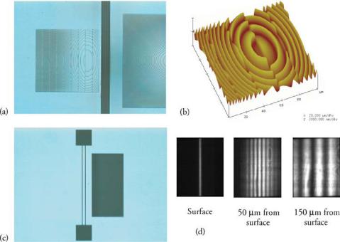
Another example of the capabilities afforded by these diffractive elements is provided by the dual-line-focus laser lens shown in the photograph and atomic force microscope scan of Fig. 17.2. This DOE was designed for the diverging-fringe shear stress sensor described in Section 17.2.2 [20]. When illuminated by the diverging field of a single-mode fiber, this DOE produces two line-foci that are coincident with slits in the chrome mask pattern on the other side of the 500 µm thick quartz substrate shown in Fig 17.2(c). The phase function of the DOE is comprised of a lens phase function that collimates along the vertical axis (in Fig. 17.2) and performs off-axis focusing along the horizontal axis, plus a binary π -phase grating that splits the focus into two equal-intensity orders that form the two line foci (low efficiency higher-orders are also created, but are blocked by the mask). This two-sided DOE was again fabricated by direct-write E-beam lithography in PMGI resist, and front-to-back
352 D. FOURGUETTE, E. ARIK, AND D. WILSON
(a) (b)
(c) |
(d) |
FIGURE 17.1. (a) Beam-shaping CGH phase, (b) Depth of CGH with lens added, (c) simulated image,
(d) measured image.
alignment marks were used to ensure alignment of the DOEs with the chrome mask pattern to an accuracy of 2 µm. Figure 17.2(d) shows photographs of the diverging fringe pattern produced when the dual-line-focus laser lens was illuminated with a single-mode output of a 660 nm fiber-pigtailed laser.
17.4. THE MINIATURE LASER DOPPLER VELOCIMETER
The miniature laser Doppler velocimeter, the MiniLDVTM, is the first step toward the miniaturization of flow sensors using a combination of refractive and diffractive optical elements. Laser Doppler velocimetry (LDV) has been in use as a research tool for over three decades. Since its inception by Yeh and Cummins [23], the LDV technique has matured to the point of being well understood and, when used carefully, providing accurate experimental data. Laser Doppler Velocimetry’s unique attributes of linear response, high frequency response (defined by the quality of the seed particles) and non-intrusiveness have made it the technique of choice for the study of complex multi-dimensional and turbulent flows [11, 15]. It has also been modified for use in multi-phase flows [16], particle sizing [2], and remote
OPTICAL MEMS-BASED SENSOR DEVELOPMENT WITH APPLICATIONS TO MICROFLUIDICS 353
FIGURE 17.2. (a) Photograph, (b) atomic-force microscope scan of the center of the dual-line-focus laser lwns,
(c) metal (chrome) mask pattern on back side of substrate, (d) diverging fringe pattern.
sensing [3], to cite a few examples. Advancements in the areas of laser performance, fiber optics, and signal processing have enhanced the utility of the technique in fluid mechanics and related research areas.
17.4.1. Principle of Measurement
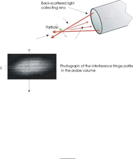
Laser Doppler velocimetry utilizes the Doppler effect to measure instantaneous particle velocities. When particles suspended in a flow are illuminated with a laser beam, the frequency of the light scattered (and/or refracted) from the particles is different from that of the incident beam. This difference in frequency, called the Doppler shift, is linearly proportional to the particle velocity. With the particle velocity being the only unknown parameter, then in principle the particle velocity can be determined from measurements of the Doppler shift f . In the commonly employed fringe mode, LDV is implemented by splitting a laser beam to have two beams intersect at a common point so that light scattered from two intersecting laser beams is mixed, as illustrated in Figure 17.3. In this way both incoming laser beams are scattered towards the receiver, but with slightly different frequencies due to the different angles of the two laser beams [1].
When two wave trains of slightly different frequency are super-imposed we get the well-known phenomenon of a beat frequency due to the two waves intermittently interfering with each other constructively and destructively. The beat frequency, also called the
354 |
|
|
|
|
|
|
|
|
|
D. FOURGUETTE, E. ARIK, AND D. WILSON |
|
|
|
|
|
|
|
|
|
|
|
|
|
|
|
|
|
|
|
|
|
|
|
|
|
|
|
Back-scattered |
|
light |
|
|
|||||
|
|
collecting lens |
|
|
|
LDV |
|||||
|
|
|
|
||||||||
|
|
|
|
|
|
|
|
|
|
|
|
|
Laser beams |
|
|
|
|
||||||
|
|
|
sensor |
||||||||
|
|
|
|
|
|
|
|
|
|||
|
|
Particle |
|
|
|
|
|
|
|
|
|
|
|
|
|
|
|
|
|
||||
|
|
|
|
|
|
|
|
|
|
||
Probe volume
Direction of the back-scattered light
|
|
Photograph of the interference fringe pattern |
δ |
|
|
|
|
in the probe volume |
|
|
|
U velocity component
FIGURE 17.3. Principle of Laser Doppler Velocimetry.
Doppler-frequency fD, corresponds to the difference between the two wave-frequencies:
f D = |
|
1 |
· 2 sin(θ /2) · ux = |
2 sin(θ /2) |
ux |
λ |
λ |
||||
where θ is the angle between the incoming laser beams and λ is the wavelength of the laser. The beat-frequency, is much lower than the frequency of the light itself, and it can be measured as fluctuations in the intensity of the light reflected from the seeding particle. As shown in the previous equation the Doppler-frequency is directly proportional to the x-component of the particle velocity, and thus can be calculated directly from fD:
λ
ux = 2 sin(θ /2) f D
Further discussion on LDA theory and different modes of operation may be found in the classic text of Durst et al. [4].
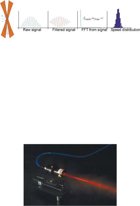
17.4.2. Signal Processing
The processing is based on the Fast Fourier Transform to extract the frequency from the burst. Figure 17.4 shows the sequence involved burst processing. The raw signal contains a DC part, low frequency component, and an AC part, high frequency component. The DC-part, which is removed by a high-pass filter, is known as the Doppler pedestal, and

356 D. FOURGUETTE, E. ARIK, AND D. WILSON
TABLE 17.1. LDV specifications
Working distance |
50 mm |
Laser wavelength |
785 nm |
Probe volume dimensions |
15 × 20 × 90 µm3 |
Fringe separation |
1.27 µm |
Number of fringes in probe volume |
14 |
Frequency shifting |
2 MHz |
|
|
then digitized using a PC-based data acquisition and processed using software developed in LabVIEWTM.
A version of the MiniLDVTM was specially designed for applications to microfluidics. Measurements in microfluidic environments generally require high spatial resolution. The probe volume size of specially designed version of the MiniLDVTM was less than 100 µm in length and 15 µm in height. The specifications for the miniature LDV sensor used to measure velocity in the microchannel are given in Table 17.1.
17.5. MICRO SENSOR DEVELOPMENT
These recent advances in micro fabrication techniques and micro-optics have enabled the development of optical microsensors for pressure and temperature, and for fluid flow measurements such as velocity and wall shear stress [6]. These microsensors offer the advantage of being non-intrusive, embeddable in small wind or water tunnel models, and capable of remote in-situ monitoring. In this Section, we describe a series of optical MEMS based microsensors for fluid flow measurements that are currently used in Research & Development settings as well as in industrial applications. These sensors are particle based, i.e., these sensors require particles to be present in the flow to scatter the light off the probe volume. The commonality for these sensors is the use of diffractive elements to shape the optical probe volume. In most cases, the generation of such optical probe volumes with conventional optics requires large optical setups prone to misalignment. Another commonality is the use of fibers to bring the light to the sensor and retrieve the backscattered signal. However, recent advances in opto-electronics will soon enable the integration of the light source and detector into the sensor head, thus bypassing the use of optical fibers.
In addition to the significant size reduction, optical MEMS provide excellent control over the shape of the probe volume, as demonstrated in the previous Section, and excellent control over the probe volume location relative to the sensor surface. Optical probe volumes generated with DOEs are diffraction limited, and most DOE designs can produce optical patterns whose characteristic length is as small as 10 micrometers. With proper optical design, a diffraction limited probe volume can be precisely and permanently positioned inside a microfluidic channel.
17.5.1. Micro Velocimeter
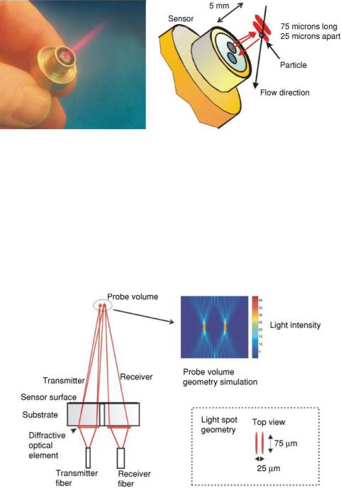
This sensor is based on time-of-flight velocity measurement technique. A photograph of the sensor, The MicroVTM, is given in Figure 17.6. The sensor optical probe volume is
OPTICAL MEMS-BASED SENSOR DEVELOPMENT WITH APPLICATIONS TO MICROFLUIDICS 357
FIGURE 17.6. Photograph of the MicroVTM (left), and schematic (right).
composed of two elongated light spots a few millimeters above the sensor surface [8]. The sensor uses one DOE to shape the optical probe volume as two elongated light spots (75 µm long and 25 µm apart) 5 mm off the sensor surface, and a second DOE to collect the backscattered light off the particles intersecting the light spots, as depicted in Figure 17.7. The height of the probe volume above the sensor surface can be designed to be anywhere between 800 µm to 20 mm.
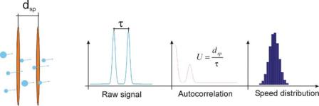
Particles present in the flow intersect the two light spots and thus generate two light bursts on the sensor detector. The resulting electric signal from the detector is two pulses that are digitized using a computer-controlled data acquisition system. Autocorrelation is
FIGURE 17.7. Schematic of the MicroVTM , results of the ray tracing simulation and schematic of the probe volume.
358 |
D. FOURGUETTE, E. ARIK, AND D. WILSON |
FIGURE 17.8. Schematic of the autocorrelation-based signal processing for the MicroV.
used to calculate the time elapsed between the two pulses, and therefore the particle velocity. A schematic of the processing algorithm is shown in Figure 17.8.
17.5.2. Micro Sensors for Flow Shear Stress Measurements
Flow shear stress measurements in biological applications have received a lot of interest in the last few years. Shear is associated with turbulence, and therefore molecular mixing. Many bio-MEMS applications involve mixing between two or more fluid channels, hence the need to understand microchannel flows in detail. In addition, regions of high shear in blood vessels exhibit high correlation with plaque deposition, and a better understanding of flows in small vessels will further the understanding of arteriosclerosis.
The wall shear stress σ is directly proportional to the velocity gradient at the wall. In the expression of the wall shear stress below,
σ = µ ∂u |
|
|
|
|
|
|
|
|
∂y y=0
µis the fluid viscosity, u is the flow velocity and y is the normal direction to the wall. The wall shear stress can be calculated by measuring the velocity gradient at the wall. In the region of the boundary layer called sub-layer, usually in the first tens of micrometers above the wall, the velocity profile is linear. Beyond the sub-layer region, the velocity profile becomes parabolic. As a result, unless the velocity is measured in the sub-layer, the velocity must be measured at a minimum of two points to calculate the velocity gradient at the wall. An iterative algorithm was successfully developed to estimate the velocity gradient at the wall using only one point velocity measurement beyond the sub-layer1. The following two Sections describe two optical MEMS based microsensors capable of measuring the fluid velocity in the boundary layer to estimate the wall shear stress.
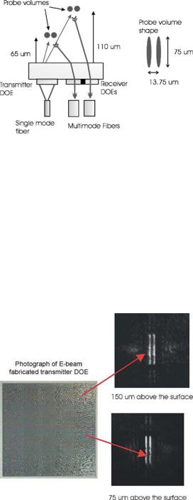
17.5.2.1.Dual Velocity Sensor A MEMS-based optical sensor was designed to measure flow velocity at two locations above the sensor surface [5]. This sensor is essentially the combination of two micro velocimeters as described in Section 17.5.1. The optical chip includes one transmitter DOE (diffractive optic element) and two receiver DOEs, as shown in Figure 17.9. As for the Micro Velocimeter, the transmitter DOE is illuminated by the output of a singe mode fiber pigtailed to a diode laser. However, the transmitter is designed
OPTICAL MEMS-BASED SENSOR DEVELOPMENT WITH APPLICATIONS TO MICROFLUIDICS 359
FIGURE 17.9. Design of the Dual Microvelocimeter with two probe volumes, one probe volume located at 65 µm and a second probe volume located at 110 µm above the surface of the sensor.
to generate two probe volumes, one located approximately at 65 µm and a second located approximately at 110 µm above the sensor surface. These probe locations are measured in air. Each probe volume is composed of two elongated light spots, 75 µm long and 13.7 µm apart. The scattered light generated by particles intersecting each probe volume, generating two intensity spikes, is focused onto a fiber by one receiver DOE and brought to an avalanche photodetector. An autocorrelation performed on the digitized output of each photodetector yields the time elapsed between the spikes. Again, as for the Micro Velocimeter, the distance between the light spots divided by the elapsed time yields the instantaneous flow velocity.
A photograph of the transmitter DOE and the resulting probe volumes generated by the transmitter are shown in Figure 17.10. The DOE was fabricated by direct-write electron
FIGURE 17.10. Photographs of the transmitter DOE and of the two probe volumes. The locations of the probe volumes are given for use in water.