

- •I. Быстрый Старт
- •Установка и запуск NL5
- •Установка NL5
- •Типы файлов
- •Запуск NL5
- •Создание и Симуляция Вашей Первой Схемы
- •Ввод схемы
- •Редактирование параметров компонентов
- •Установки переходного процесса (transient)
- •Данные переходного процесса
- •Запуск анализа переходного процесса
- •Установки частотной характеристики (AC)
- •Данные AC
- •Запуск AC анализа
- •Лицензия NL5
- •Single PC License
- •Portable License
- •Network License
- •Personal License
- •II. Интерфейс Пользователя
- •Графический Интерфейс Пользователя
- •Основное Окно
- •Основное Меню (Main Menu)
- •Основная инструментальная панель (Main Toolbar)
- •Строка состояния (Status Bar)
- •Панель выбора (Selection Bar)
- •Панель навигации
- •Окна документа
- •Другие окна
- •Окна диалогов
- •Помощь (Help)
- •Горячие клавиши
- •Предпочтения (Preferences)
- •Preferences (предпочтения)
- •Application (приложение)
- •Document (документ)
- •Schematic (схема)
- •Drawings (рисунки)
- •Mouse (Schematic) (мышь, схема)
- •Components (компоненты)
- •Symbols (символы компонентов)
- •Warnings (предупреждения)
- •Graphs (графики)
- •Table (таблица)
- •Legend (условные обозначения, список кривых на графике)
- •Annotation (аннотация)
- •Text (текст)
- •Mouse (Graphs) (мышь, графики)
- •Transient (переходный процесс)
- •HTTP Server
- •Печать
- •Форматирование печати
- •Формат данных
- •Нечувствительность к регистру (case-insensitivity).
- •Числа
- •Имена
- •Операторы
- •Функции
- •Выражения
- •Язык C
- •Comments (комментарии)
- •Data types (типы данных)
- •Variables (переменные)
- •Arrays (массивы)
- •Statements and operators
- •Скрипт
- •Синтаксис
- •Команды
- •Примеры скрипта
- •III. Схема
- •Окно схемы
- •Редактирование схемы
- •Курсор
- •Проводник
- •Соединение (Connection)
- •Земля
- •Компонент
- •Вид компонента (View)
- •Этикетка (Label)
- •Атрибуты
- •Рисунки (линия, прямоугольник, овал)
- •Текст и Переменные
- •Прокрутка и масштабирование
- •Выделение и сброс выделения
- •Удаление
- •Перемещение и копирование
- •Отключить и включить (Disable and Enable)
- •Повернуть, отразить, перевернуть (Rotate, Mirror, Flip)
- •Формат
- •Отменить и выполнить повторно (Undo, Redo)
- •Команды редактирования схемы
- •Клавиатура и горячие клавиши
- •Операции с мышкой
- •Компоненты и модели
- •Формулы
- •Функции
- •Редактирование конфигурируемого компонента (customized)
- •Работа с подсхемами
- •Работа с PWL моделью
- •Работа с PWL источником
- •Работа с моделью List
- •Работа с моделью Table
- •Работа с двухмерной (2D) моделью Table
- •Работа с моделью C
- •Работа с моделью DLL
- •Окно Компонентов (Componets Window)
- •Инструментальная панель
- •Список компонентов
- •Выбор модели
- •Редактирование параметров
- •Окно переменных (Variables Window)
- •Панель инструментов
- •Редактирование переменных
- •Листы (Sheets)
- •Группы
- •Проверка схемы
- •Инструменты схемы
- •Renumber (перенумерация)
- •Initial Conditions (начальные условия)
- •Clean Up (чистка)
- •Formulas (формулы)
- •Parameters (параметры)
- •Transform (преобразование)
- •Свойства (Properties)
- •Симуляция
- •Алгоритм симуляции
- •Данные симуляции
- •Установки переходного процесса (Transient Settings)
- •Advanced Settings
- •Данные переходного процесса (Transient Data)
- •Инструментальная панель
- •Traces (кривые)
- •Симуляция
- •Окно переходного процесса (Transient window)
- •График
- •Legend (условные обозначения)
- •Курсоры
- •Текст
- •Storage (накопитель данных, «хранилище»)
- •Data table (Таблица данных)
- •Прокрутка и масштабирование
- •Команды переходного процесса
- •Клавиатура и горячие клавиши
- •Операции с мышкой
- •Инструменты переходного процесса (Transient Tools)
- •DC sweep
- •XY diagram (XY-диаграмма)
- •Amplitude histogram (амплитудная гистограмма)
- •Histogram (гистограмма)
- •FFT (Быстрое Преобразование Фурье)
- •Eye diagram (Глазковая диаграмма)
- •Markers (маркеры)
- •Power (мощность)
- •Line snapshot
- •V. Частотная Характеристика (AC)
- •Симуляция
- •Метод линеаризации схемы
- •Метод «включения» источника (Sweep AC source)
- •Z-преобразование (Z-transform)
- •Данные симуляции
- •Установки AC (AC Settings)
- •Advanced Settings
- •Данные AC (AC Data)
- •Инструментальная панель
- •Traces (кривые)
- •Выполнение симуляции
- •Окно AC (AC window)
- •График
- •Legend (условные обозначения)
- •Курсоры
- •Text.
- •Storage (накопитель данных)
- •Data table (Таблица данных)
- •Прокрутка и масштабирование
- •Команды AC
- •Клавиатура и горячие клавиши
- •Операции с мышкой
- •Инструменты AC (AC Tools)
- •Histogram (гистограмма)
- •Smith Chart (Диаграмма Смита)
- •Диаграмма Найквиста
- •Диаграмма Николса
- •Markers (маркеры)
- •VI. Инструменты (Tools)
- •Скрипт
- •Выполнение скрипта
- •Console (консоль)
- •Командная строка
- •Sweep (серия)
- •Оптимизация
- •HTTP link
- •Запуск HTTP сервера
- •Посылка URL запроса
- •Запуск симуляция
- •Пример связи NL5-MATLAB
- •VII. Приложения (Attachments)
- •Label
- •2. Operators
- •3. Functions
- •4. Script commands
- •5. END USER LICENSE AGREEMENT
NL5 circuit simulator |
Руководство Пользователя |
VII. Приложения (Attachments)
Приложения, как содержащие сугубо техническую информацию, не переведены.
302
NL5 circuit simulator |
Руководство Пользователя |
1. Component Types, Models and Parameters
Component types are described in the following format:
Letter |
|
Type |
Models |
Model 1 |
|
|
|
Symbol |
Model 2 |
||
|
|
|
|
|
|
|
|
|
|
|
… |
|
|
|
|
|
|
Views |
View 1 |
View 2 |
… |
||
|
|
||||
|
|
|
|
|
|
|
|
|
(optional) |
|
|
|
|
|
|
|
|
Traces |
Picture of |
|
V, I, P traces |
||
|
||
|
|
Description of views (optional)
Model and parameters are presented as follows:
Letter |
|
Type |
|
|
|
Examples/Components/Example file name |
|
|
|
|
|
|
|
|
|
Model |
|
|
Parameter |
Units |
Description |
||
|
|
|
|
|
|
||
Model |
|
|
Par 1 |
Unit 1 |
Par 1 description |
||
name |
|
|
Par 2 |
Unit 2 |
Par 2 description |
||
|
|
|
|
|
|
||
|
|
… |
… |
… |
|||
|
|
|
|
||||
Model |
|
|
|
|
|
|
|
|
|
|
|
|
|
||
specific |
|
Detailed description of the model and parameters. |
|||||
view |
|
|
|||||
|
|
|
|
|
|
||
(optional) |
|
|
|
|
|
||
|
|
|
|
|
|
|
|
Model example files are located in the Examples/Components folder of the NL5 complete package download zip file.
303
NL5 circuit simulator |
Руководство Пользователя |
Label
Models
Label
V
Pulse
Step
Sin
PWL
Function
File
Trace
SubCir
I
V
Traces
P = V • I
|
Label |
|
|
|
|
Label/Label_Label.nl5 |
|
|
|
|
|
|
|
||
Model |
Parameter |
Units |
Description |
||||
|
|
|
|
|
|
||
Label |
VIC |
|
V |
Initial condition: initial voltage. |
|||
|
|
|
|
|
|||
R |
|
Ohm |
Initial resistance. |
||||
|
|
|
|||||
|
|
|
|
|
|||
|
|
Label. This model can be used: |
|||||
|
|
- |
As a voltage trace probe point. |
||||
|
|
- |
For connecting schematic points without wires, including points at different sheets. |
||||
|
|
- |
To apply initial voltage during DC operating point calculation. |
||||
|
|
When calculating DC operating point, if initial voltage “VIC” is not blank, the temporary voltage |
|||||
|
|
source “VIC” is connected to the label through initial resistor “R”. When DC operating point is |
|||||
|
|
found, the voltage source is removed. Initial voltage “VIC” is cleared by “Transient/Save IC” |
|||||
|
|
command. |
|
|
|
||
|
|
Please note: “VIC” is not a constant voltage source! This voltage will be removed after DC |
|||||
|
|
operating point calculation, and the label will be floating! For constant voltage source use V |
|||||
|
|
model. |
|
|
|
|
|
|
|
|
|
|
|
|
|
|
|
|
|
|
|
|
|
|
Label |
|
|
|
|
Label/Label_V.nl5 |
|
|
|
|
|
|
|
||
Model |
Parameter |
Units |
Description |
||||
|
|
|
|
|
|
||
V |
V |
|
V |
Voltage. |
|||
|
|
|
|
|
|||
Constant voltage source. Voltage = “V”. |
|||||||
|
|
||||||
|
|
|
|
|
|
|
|
304

NL5 circuit simulator |
|
|
Руководство Пользователя |
|
||
|
|
|
|
|
|
|
|
Label |
|
|
|
Label/Label_Pulse.nl5 |
|
|
|
|
|
|
|
|
Model |
Parameter |
Units |
Description |
|
||
|
|
|
|
|
|
|
Pulse |
V1 |
V |
Pulse On voltage. |
|
||
|
|
|
|
|
||
V0 |
V |
Pulse Off voltage. |
|
|||
|
|
|
||||
|
|
|
|
|
|
|
|
|
Period |
s |
Period. |
|
|
|
|
|
|
|
|
|
|
|
Width |
s |
Pulse width. |
|
|
|
|
|
|
|
|
|
|
|
Slope |
|
Slope type: Linear/Cos/Exp |
|
|
|
|
|
|
|
|
|
|
|
Rise |
s |
Pulse rise length. |
|
|
|
|
|
|
|
|
|
|
|
Fall |
s |
Pulse fall length. |
|
|
|
|
|
|
|
|
|
|
|
Delay |
s |
Delay before first pulse starts. |
|
|
|
|
|
|
|
|
|
Pulse voltage source. Pulses start after “Delay” time. “Rise” time is included into “Width”, “Fall” time is not included into “Width”. Almost every parameter can be set to zero and infinity (“inf”); otherwise the error message will be displayed.
Slope type applies both to pulse rise and fall. The following slope types are available:
Linear |
Cos (cosine) |
Exp (exponential) |
305

NL5 circuit simulator |
|
|
Руководство Пользователя |
|
||
|
|
|
|
|
|
|
|
Label |
|
|
|
Label/Label_Step.nl5 |
|
|
|
|
|
|
|
|
Model |
Parameter |
Units |
Description |
|
|
|
|
|
|
|
|
|
|
Step |
V1 |
V |
Step On voltage. |
|
|
|
|
|
|
|
|
||
V0 |
V |
Step Off voltage. |
|
|
||
|
|
|
|
|||
|
|
|
|
|
|
|
|
|
Slope |
|
Slope type: Linear/Cos/Exp |
|
|
|
|
|
|
|
|
|
|
|
Rise |
s |
Step rise length. |
|
|
|
|
|
|
|
|
|
|
|
Delay |
s |
Delay before step starts. |
|
|
|
|
|
|
|
|
|
|
|
Step voltage source. Step starts after “Delay” time. |
|
|||
|
|
The following slope types are available: |
|
|
||
|
|
Linear |
|
Cos (cosine) |
Exp (exponential) |
|
|
|
|
|
|
|
|
306
NL5 circuit simulator |
|
|
|
Руководство Пользователя |
|
||
|
|
|
|
|
|
|
|
|
Label |
|
|
|
|
Label/Label_Sin.nl5 |
|
|
|
|
|
|
|
|
|
Model |
Parameter |
|
Units |
Description |
|
||
|
|
|
|
|
|
|
|
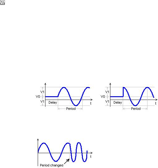
Sin |
V1 |
|
V |
Voltage amplitude. |
|
||
|
|
|
|
|
|
||
V0 |
|
V |
Voltage baseline. |
|
|||
|
|
|
|
||||
|
|
|
|
|
|
|
|
|
|
Period |
|
s |
Period. |
|
|
|
|
|
|
|
|
|
|
|
|
Phase |
|
deg |
Phase. |
|
|
|
|
|
|
|
|
|
|
|
|
Delay |
|
s |
Delay before sine signal starts. |
|
|
|
|
|
|
|
|
||
|
|
Sine voltage source. Sine signal starts after “Delay” time. “Phase” is sine phase in degrees |
|
||||
|
|
at the moment when signal starts: |
|
||||
|
|
|
Phase = 0 |
|
Phase = 90 |
|
|
|
|
If transient is paused, sine period changed, then transient is continued, the phase of the signal |
|
||||
|
|
remains continuous, providing smooth sine signal of variable frequency: |
|
||||
|
|
|
|
|
|
|
|
307
NL5 circuit simulator |
|
|
Руководство Пользователя |
|
||
|
|
|
|
|
|
|
|
Label |
|
|
|
Label/Label_PWL.nl5 |
|
|
|
|
|
|
|
|
Model |
Parameter |
Units |
Description |
|
||
|
|
|
|
|
|
|
PWL |
pwl |
|
Comma-separated string. |
|
||
|
|
|
|
|
||
Cycle |
|
Cycling (repeat): No/Yes. |
|
|||
|
|
|
|
|||
|
|
|
|
|
|
|
|
|
Delay |
s |
Delay. |
|
|
|
|
|
|
|
|
|
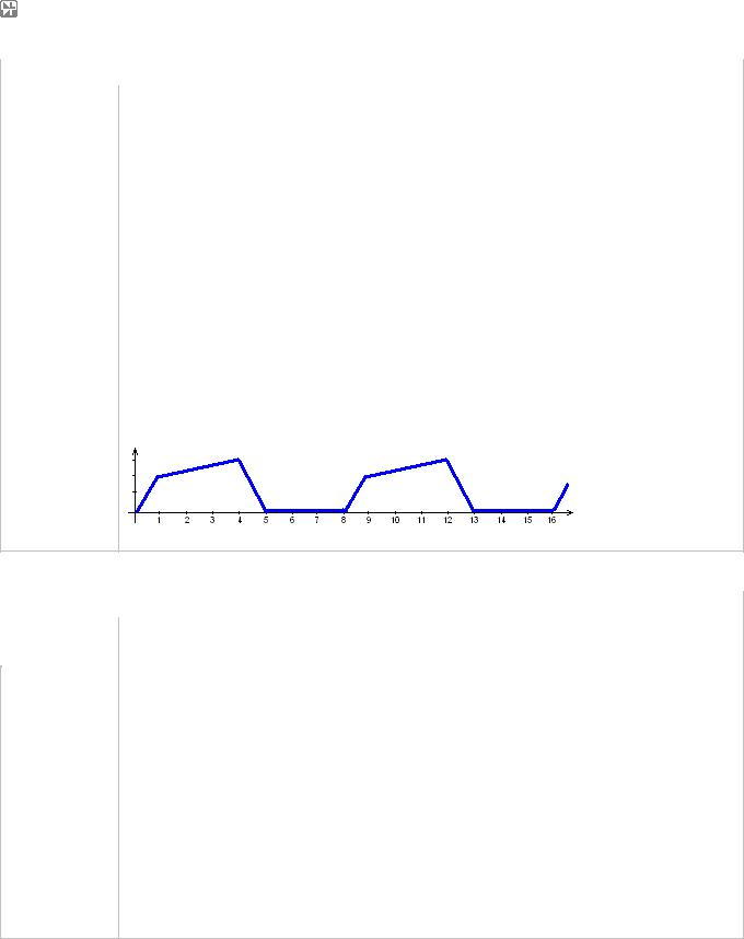
Piece-wise linear voltage source. Signal is defined by “pwl” parameter in the csv (“commaseparated values”) format, as follows:
t0,V0,t1,V1,...,tn,Vn
where all t and V can be numerical values or expressions. If t<t0, signal is V0. If t0<t<t1, signal value is linearly interpolated between V0 and V1, etc. If t>tn, then signal value is Vn if “Cycle” parameter is set to “No”, otherwise signal defined in t0…tn interval is repeated continuously. In addition, the whole signal is delayed by “Delay” time.
Example:
pwl = 0,0,1,2,4,3,5,0,8,0
If “Cycle” = Yes, “Delay” = 0, the following voltage will be generated:
|
|
Label |
|
|
|
Label/Label_Function.nl5 |
|
|
|
|
|
|
|
|
Model |
Parameter |
Units |
Description |
||
|
|
|
|
|
|
|
|
Function |
F(t) |
V |
Function |
||
|
Arbitrary function. F(t) defines voltage as a function of the following variables: |
|||||
|
|
|
||||
t - current time
V(name) - voltage on the component name I(name) - current through the component name P(name) – power on the component name
where name is the name of any component in the schematic. If F(t) is blank, voltage is zero.
Example:
F(t) = sin(t) * (1+cos(t*.01))
F(t) = V(R1) * I(R1)
Please note that V, I, and P variables are taken at previous calculation step. This may affect stability of the schematic with closed loop.
308

NL5 circuit simulator |
|
|
Руководство Пользователя |
|
||
|
|
|
|
|
|
|
|
Label |
|
|
|
Label/Label_File.nl5 |
|
|
|
|
|
|
|
|
Model |
Parameter |
Units |
Description |
|
||
|
|
|
|
|
|
|
File |
File |
|
File name. |
|
||
|
|
|
|
|
||
Cycle |
|
Cycling (repeat): No/Yes. |
|
|||
|
|
|
|
|||
|
|
|
|
|
|
|
|
|
Delay |
s |
Delay. |
|
|
|
|
|
|
|
|
|
Voltage source defined in the text file. “File“ parameter is a file name, with full path to the file. If the file is located in the same directory as schematic file, the path can be omitted. Signal is defined in the csv (“comma-separated values”) format, as follows:
<if first line does not start with a number, it is ignored > t0,V0
t1,V1
.....
tn,Vn
where all t and V can be numerical values or expressions. If t<t0, signal is V0. If t0<t<t1, signal value is linearly interpolated between V0 and V1, etc. If t>tn, then signal value is Vn if “Cycle” parameter is set to “No”, otherwise signal defined in t0…tn interval is repeated continuously. In addition, the whole signal is delayed by “Delay” time.
Example:
0,0
1,2
4,3
5,0
8,0
If “Cycle” = Yes, “Delay” = 0, the following voltage will be generated:
|
Label |
|
|
|
Label/Label_Trace.nl5 |
|
|
|
|
|
|
Model |
Parameter |
Units |
Description |
||
|
|
|
|
|
|
Trace |
Trace |
|
Trace name. |
||
|
|
|
|
||
Cycle |
|
Cycling (repeat): No/Yes. |
|||
|
|
|
|||
|
|
|
|
|
|
|
|
Delay |
s |
Delay. |
|
|
|
|
|
|
|
|
|
Voltage source defined by a trace. “Trace” parameter is a name of the trace in the Trace list |
|||
|
|
(Transient/Data). Only traces loaded from data file, imported from text or binary file, |
|||
|
|
duplicated, or pasted from clipboard can be used for he voltage source. If “Cycle” parameter is |
|||
|
|
set to “Yes”, the signal is repeated continuously. In addition, the whole signal is delayed by |
|||
|
|
“Delay” time. |
|
|
|
|
|
|
|
|
|
309
NL5 circuit simulator |
|
|
Руководство Пользователя |
|
||
|
|
|
|
|
|
|
|
Label |
|
|
|
Label/Label_SubCir.nl5 |
|
|
|
|
|
|
|
|
Model |
Parameter |
Units |
Description |
|
||
|
|
|
|
|
|
|
SubCir |
File |
|
File name of subcircuit schematic. |
|
||
|
|
|
|
|
||
Pin1 |
|
Name of subcircuit label connected to pin 1 |
|
|||
|
|
|
|
|||
|
|
|
|
|
|
|
|
|
Cmd |
|
Subcircuit start-up command string |
|
|
|
|
|
|
|
|
|
|
|
IC |
|
Subcircuit Initial conditions string |
|
|
|
|
|
|
|
|
|
|
|
Subcircuit. See Working with Subcircuits chapter for details. |
|
|||
|
|
|
|
|
|
|
310

NL5 circuit simulator |
Руководство Пользователя |
A |
Amperemeter |
|
|
|
I |
|
Amperemeter |
|
|
||
|
|
|
|
||
|
|
Models |
|
Traces |
|
|
|
|
|
|
P = V • I |
|
|
|
|
|
|
V
A |
Amperemeter |
|
A/ A_Amperemeter_Amperemeter.nl5 |
|
|
|
|
|
Model |
No parameters |
|
Amperemeter |
Amperemeter. Short circuit. In addition to current, amperemeter can measure voltage |
|
|
|
relative to ground, and power to grounded load. |
311
NL5 circuit simulator |
Руководство Пользователя |
C Capacitor
Models
C
PWL
Function
SubCir
Traces
V  I
I
P = V • I
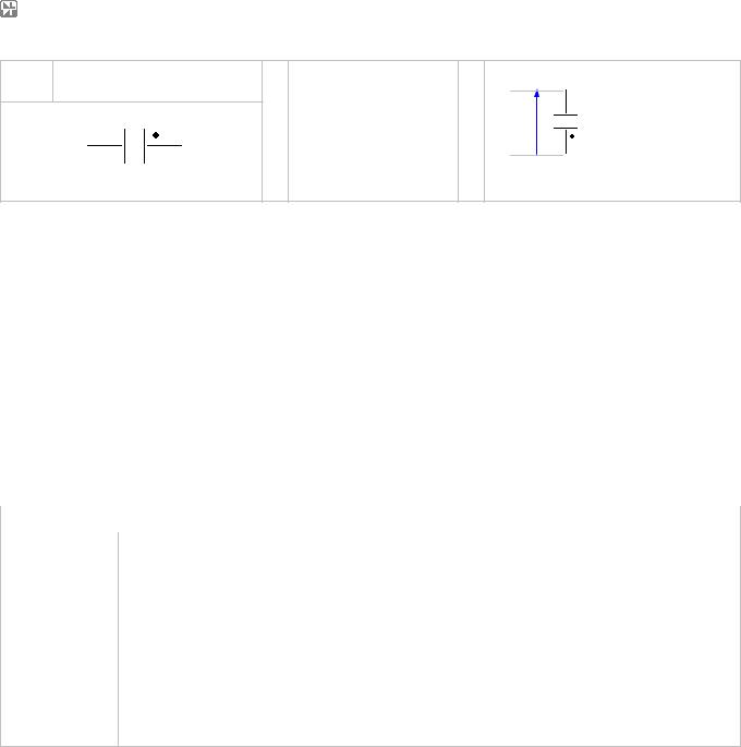
C |
|
Capacitor |
|
|
|
C/C_Capacitor_C.nl5 |
|
|
|
|
|
|
|
|
|
|
Model |
|
Parameter |
Units |
Description |
||
|
|
|
|
|
|
|
|
|
C |
|
C |
F |
Capacitance |
||
|
|
|
|
|
|
||
|
|
IC |
V |
Initial condition: voltage. Leave blank if IC not defined. |
|||
|
|
|
|
||||
|
|
|
|
|
|
|
|
|
|
|
|
Linear capacitor. I = C*dV/dt. |
|||
|
|
|
|
When calculating DC operating point, if “IC” is defined, capacitor is replaced with voltage |
|||
|
|
|
|
source equal to IC. If “IC” is not defined (blank), capacitor is temporarily removed (open |
|||
|
|
|
|
circuit), DC operating point calculated, and then the voltage found across the capacitor is |
|||
|
|
|
|
assigned to the capacitor as its initial voltage. |
|||
|
|
|
|
|
|
|
|
|
|
|
|
|
|
|
|
C |
|
Capacitor |
|
|
|
C/C_Capacitor_PWL.nl5 |
|
|
|
|
|
|
|
|
|
|
Model |
Parameter |
Units |
Description |
|||
|
|
|
|
|
|
|
|
|
PWL |
|
pwl |
|
Comma-separated string, C(V) |
||
|
|
|
|
|
|
||
|
|
IC |
V |
Initial condition: voltage. Leave blank if no IC defined. |
|||
|
|
|
|
||||
|
|
|
|
|
|
|
|
Piece-wise linear capacitor. “pwl” string defines capacitance as a function of voltage. See
Working with PWL model chapter for details.
When calculating DC operating point, if “IC” is defined, capacitor is replaced with voltage source equal to IC. If “IC” is not defined (blank), capacitor is temporarily removed (open circuit), DC operating point calculated, and then the voltage found across the capacitor is assigned to the capacitor as its initial voltage.
312

NL5 circuit simulator |
|
|
Руководство Пользователя |
|
||||
|
|
|
|
|
|
|
|
|
C |
|
Capacitor |
|
|
|
C/C_Capacitor_Function.nl5 |
|
|
|
|
|
|
|
|
|
|
|
|
Model |
|
Parameter |
Units |
Description |
|
||
|
|
|
|
|
|
|
|
|
Function |
|
Z(s) |
Ohm |
Impedance as a function of s parameter. |
|
|||
|
|
|
|
|
|
|||
|
Impedance function in s domain. For transient, constant impedance Z(0) is used. For |
|
||||||
|
|
|
|
|
||||
|
|
|
|
linearized AC analysis, complex impedance Z(s) is used. The following variables can be used |
|
|||
|
|
|
|
in the function: |
|
|
|
|
|
|
|
|
f – current AC frequency, Hz |
|
|||
|
|
|
|
w – angular AC frequency, w = 2πf . |
|
|||
|
|
|
|
s or p – Laplace parameter, s = p = j*2πf. |
|
|||
|
|
|
|
z – Z-transform parameter, is defined by custom formula in the Advanced Settings |
|
|||
|
|
|
|
dialog box. |
|
|
|
|
|
|
|
|
Example: |
|
|
|
|
|
|
|
|
Z(s) = 1.0/3p/s + 1.5p - 3 pF capacitor in series with 1.5 pH inductor. |
|
|||
|
|
|
|
Z(s) = (1.0/10n/s)||1k - 10 nF capacitor in parallel with 1 kOhm resistor. |
|
|||
|
|
|
|
|
|
|
|
|
|
|
|
|
|
|
|
|
|
C |
|
Capacitor |
|
|
|
C/C_Capacitor_SubCir.nl5 |
|
|
|
|
|
|
|
|
|
|
|
|
Model |
|
Parameter |
Units |
Description |
|
||
|
|
|
|
|
|
|
|
|
SubCir |
|
File |
|
File name of subcircuit schematic. |
|
|||
|
|
|
|
|
|
|||
|
Pin1 |
|
Name of subcircuit label connected to pin 1 |
|
||||
|
|
|
|
|
|
|||
|
|
|
|
|
|
|
|
|
|
|
|
|
Pin2 |
|
Name of subcircuit label connected to pin 2 |
|
|
|
|
|
|
|
|
|
|
|
|
|
|
|
Cmd |
|
Subcircuit start-up command string |
|
|
|
|
|
|
|
|
|
|
|
|
|
|
|
IC |
|
Subcircuit Initial conditions string |
|
|
|
|
|
|
|
|
|
|
|
|
|
|
|
Subcircuit. See Working with Subcircuits chapter for details. |
|
|||
|
|
|
|
|
|
|
|
|
313

NL5 circuit simulator |
Руководство Пользователя |
C |
Voltage controlled |
|
PWL |
|
capacitor |
|
|
||
|
|
|
||
|
|
Models |
|
Traces |
|
|
|
|
|
Views
V in |
V I |
|||
|
|
|
|
|
P = V • I |
|
|
||
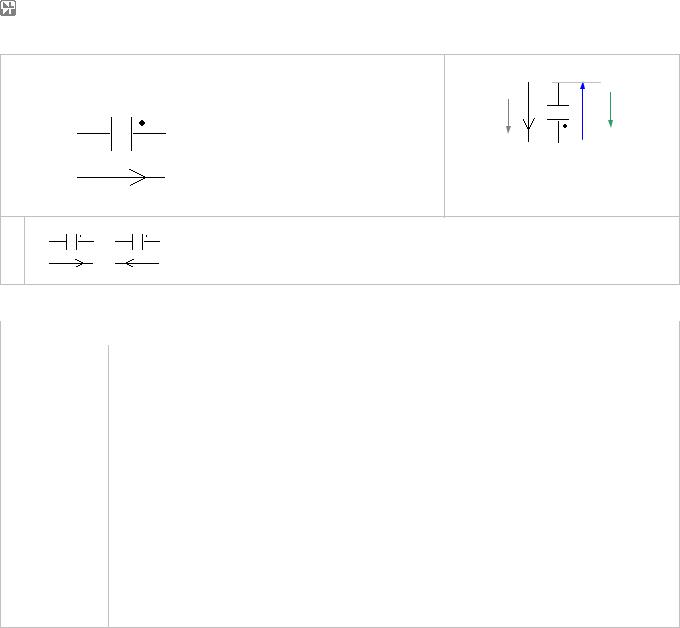
C |
|
Voltage controlled capacitor |
|
C/C_VCC_PWL.nl5 |
||
|
|
|
|
|
|
|
|
Model |
Parameter |
Units |
Description |
||
|
|
|
|
|
|
|
|
PWL |
pwl |
|
Comma-separated string, C(Vin) |
||
|
|
|
|
|
||
|
IC |
V |
Initial condition: voltage. Leave blank if IC not defined. |
|||
|
|
|
||||
|
|
|
|
|
|
|
Piece-wise linear voltage controlled capacitor. At any moment, capacitor is a linear capacitor. Its capacitance C is a function of control voltage:
I = C(Vin)*dV/dt.
“pwl” string defines capacitance as a function of control voltage Vin. See Working with PWL model chapter for details.
When calculating DC operating point, if “IC” is defined, capacitor is replaced with voltage source equal to IC. If “IC” is not defined (blank), capacitor is temporarily removed (open circuit), DC operating point calculated, and then the voltage found across the capacitor is assigned to the capacitor as its initial voltage.
314
NL5 circuit simulator |
Руководство Пользователя |
C |
Current controlled |
|
PWL |
|
capacitor |
|
|
||
|
|
|
||
|
|
Models |
|
Traces |
|
|
|
|
|
Views
I in |
V I |
|
P = V • I |
|
|
|
|
|
C |
|
Current controlled capacitor |
|
C/C_CCC_PWL.nl5 |
||
|
|
|
|
|
|
|
|
Model |
Parameter |
Units |
Description |
||
|
|
|
|
|
|
|
|
PWL |
pwl |
|
Comma-separated string, C(Iin) |
||
|
|
|
|
|
||
|
IC |
V |
Initial condition: voltage. Leave blank if IC not defined. |
|||
|
|
|
||||
|
|
|
|
|
|
|
Piece-wise linear current controlled capacitor. At any moment, capacitor is a linear capacitor. Its capacitance C is a function of control current:
I = C(Iin)*dV/dt.
“pwl” string defines capacitance as a function of control current Iin. See Working with PWL model chapter for details.
When calculating DC operating point, if “IC” is defined, capacitor is replaced with voltage source equal to IC. If “IC” is not defined (blank), capacitor is temporarily removed (open circuit), DC operating point calculated, and then the voltage found across the capacitor is assigned to the capacitor as its initial voltage.
315
NL5 circuit simulator |
Руководство Пользователя |
D
Diode
Models
Diode
Storage
Soft
PWL
SubCir
Traces
V  I
I
P = V • I
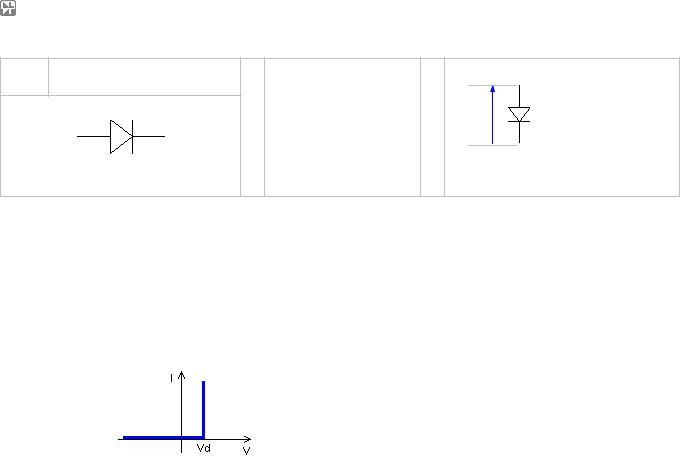
D |
|
Diode |
|
|
|
D/D_Diode_Diode.nl5 |
|
|
|
|
|
|
|
|
Model |
Parameter |
Units |
Description |
||
|
|
|
|
|
|
|
Diode |
Vd |
V |
Forward voltage drop. |
|||
|
|
|
|
|||
IC |
|
Initial condition: On/Off. |
||||
|
|
|
|
|||
|
|
|
|
|
|
|
|
|
|
Ideal diode. If V >= “Vd”, diode is On (short circuit). Otherwise diode is Off (open circuit, I=0). |
|||
|
|
|
When calculating DC operating point diode is set to the state specified in “IC”. |
|||
|
|
|
|
|
|
|
316
NL5 circuit simulator |
|
|
Руководство Пользователя |
|
|||
|
|
|
|
|
|
|
|
D |
|
Diode |
|
|
|
D/D_Diode_Storage.nl5 |
|
|
|
|
|
|
|
|
|
|
Model |
Parameter |
Units |
Description |
|
||
|
|
|
|
|
|
|
|
Storage |
Vd |
V |
Forward voltage drop. |
|
|||
|
|
|
|
|
|||
t |
s |
Recombination time constant. |
|
||||
|
|
|
|
||||
|
|
|
|
|
|
|
|
|
|
|
IC |
|
Initial condition: Off/On. |
|
|
|
|
|
|
|
|
|
|
|
|
|
ICQ |
C (A*s) |
Initial condition: charge. |
|
|
|
|
|
|
|
|
|
|
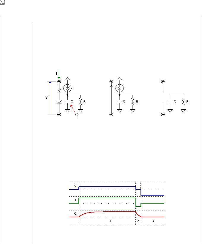
Charge storage diode. Simplified equivalent schematic of the model is the following:
1. Forward current |
2. Reverse current |
3. No current |
V = ”Vd”, I > 0, Q > 0 |
V = 0, I < 0, Q > 0 |
V < 0, I = 0, Q = 0 |
The diode has internal capacitor C and resistor R, with the time constant RC = “t”, Q is the charge on the capacitor. In mode 1, forward current flows through the diode and forward voltage drop is “Vd”. At the same time, the current equal to forward current is charging capacitor C. In mode 2, reverse current is applied to the diode, and capacitor C is being discharged by the current equal to reverse current. As long as charge Q on the capacitor is positive, the diode is a short circuit with zero voltage drop. Finally, when charge drops to zero, the diode switches to mode 3, with zero current and negative voltage drop (open circuit). V, I, and Q waveforms are shown on the graph:
When calculating DC operating point the diode is set to the state specified in “IC”, and internal charge Q is set to specified “ICQ” value.
317
NL5 circuit simulator |
|
|
Руководство Пользователя |
|
|||
|
|
|
|
|
|
|
|
D |
|
Diode |
|
|
|
D/D_Diode_Soft.nl5 |
|
|
|
|
|
|
|
|
|
|
Model |
Parameter |
Units |
Description |
|
||
|
|
|
|
|
|
|
|
|
Soft |
Vd |
V |
Forward voltage drop. |
|
||
|
|
|
|
|
|
||
|
t |
s |
Recombination time constant. |
|
|||
|
|
|
|
||||
|
|
|
|
|
|
|
|
|
|
|
ts |
s |
Soft recovery time constant. |
|
|
|
|
|
|
|
|
|
|
|
|
|
IC |
|
Initial condition: Off/On. |
|
|
|
|
|
|
|
|
|
|
|
|
|
ICQ |
C (A*s) |
Initial condition: charge. |
|
|
|
|
|
|
|
|
|
|
Soft recovery charge storage diode. Simplified equivalent schematic of the model is the following:
1. Forward current |
2. Reverse current |
3. Soft recovery |
V = “Vd”, I > 0, Q > 0 |
V = “Vd”, I < 0, Q > 0 |
V < “Vd”, I < 0, Q > 0 |
C = 1, R = “t” |
C = 1, R = “t” |
C = 1, R = “ts” |
The diode has internal capacitor C=1 and resistor R. Time constant RC is equal either recombination time constant “t”, or soft recovery time constant= “ts”. Q is the charge on the capacitor. In mode 1, forward current flows through the diode and forward voltage drop is “Vd”. At the same time, the current equal to forward current is charging capacitor C. In mode 2, reverse current is applied to the diode, and capacitor C is being discharged by the current equal to reverse current. Voltage drop on the diode is still “Vd”. At the moment when reverse current is equal or less than charge divided by soft recovery time constant “ts”, a mode 3 is turned on. In mode 3, capacitor C is being exponentially discharged by the current through resistor R with time constant “ts” (plus small constant current to ensure full discharge - not shown on the picture). Reverse diode current is proportional to the charge. As soon as charge drops to zero, the diode switches to mode 4 (not shown), with zero current and negative voltage drop (open circuit). See demo schematic D/D_Diode_Soft.nl5 for examples of soft recovery waveforms.
When calculating DC operating point the diode is set to the state specified in “IC”, and internal charge Q is set to specified “ICQ” value.
318

NL5 circuit simulator |
|
|
Руководство Пользователя |
|
|||
|
|
|
|
|
|
|
|
D |
|
Diode |
|
|
|
D/D_Diode_PWL.nl5 |
|
|
|
|
|
|
|
|
|
|
Model |
Parameter |
Units |
Description |
|
||
|
|
|
|
|
|
|
|
|
PWL |
pwl |
|
Comma-separated string, R(V) |
|
||
|
|
|
|
|
|
||
|
Piece-wise linear diode. “pwl” string defines resistance as a function of voltage. See Working |
|
|||||
|
|
|
|
||||
|
|
|
with PWL model chapter for details. |
|
|||
|
|
|
|
|
|
|
|
|
|
|
|
|
|
|
|
D |
|
Diode |
|
|
|
D/D_Diode_SubCir.nl5 |
|
|
|
|
|
|
|
|
|
|
Model |
Parameter |
Units |
Description |
|
||
|
|
|
|
|
|
|
|
SubCir |
File |
|
File name of subcircuit schematic. |
|
|||
|
|
|
|
|
|||
Pin1 |
|
Name of subcircuit label connected to pin 1 |
|
||||
|
|
|
|
|
|||
|
|
|
|
|
|
|
|
|
|
|
Pin2 |
|
Name of subcircuit label connected to pin 2 |
|
|
|
|
|
|
|
|
|
|
|
|
|
Cmd |
|
Subcircuit start-up command string |
|
|
|
|
|
|
|
|
|
|
|
|
|
IC |
|
Subcircuit Initial conditions string |
|
|
|
|
|
|
|
|
|
|
Subcircuit. See Working with Subcircuits chapter for details.
319
NL5 circuit simulator |
Руководство Пользователя |
D
Zener
Models
Zener
PWL
SubCir
Traces
V  I
I
P = V • I
D |
|
Zener |
|
|
|
D/D_Zener_Zener.nl5 |
|
|
|
|
|
|
|
|
|
|
Model |
Parameter |
Units |
Description |
|||
|
|
|
|
|
|
||
Zener |
V |
V |
Breakdown voltage drop. |
||||
|
|
|
|
||||
Vd |
V |
Forward voltage drop. |
|||||
|
|
|
|||||
|
|
|
|
|
|
||
|
|
|
IC |
|
Initial condition: Minus/Off/Plus. |
||
|
|
|
|
|
|
||
|
|
|
Ideal zener. If V <= -“V” or V >= “Vd”, zener is On (short circuit). Otherwise zener is Off (open |
||||
|
|
|
circuit, I=0). |
|
|
|
|
|
|
|
When calculating DC operating point zener is set to the state specified in “IC”. |
||||
|
|
|
|
|
|
|
|
|
|
|
|
|
|
|
|
D |
|
Zener |
|
|
|
D/D_Zener_PWL.nl5 |
|
|
|
|
|
|
|
|
|
|
Model |
Parameter |
Units |
Description |
|||
|
|
|
|
|
|
||
|
PWL |
pwl |
|
Comma-separated string, R(V) |
|||
|
|
|
|
|
|||
|
Piece-wise linear zener. “pwl” string defines resistance as a function of voltage. See Working |
||||||
|
|
|
|||||
|
|
|
with PWL model chapter for details. |
||||
|
|
|
|
|
|
|
|
|
|
|
|
|
|
|
|
D |
|
Zener |
|
|
|
D/D_Zener_SubCir.nl5 |
|
|
|
|
|
|
|
|
|
|
Model |
Parameter |
Units |
Description |
|||
|
|
|
|
|
|
||
SubCir |
File |
|
File name of subcircuit schematic. |
||||
|
|
|
|
||||
Pin1 |
|
Name of subcircuit label connected to pin 1 |
|||||
|
|
|
|
||||
|
|
|
|
|
|
||
|
|
|
Pin2 |
|
Name of subcircuit label connected to pin 2 |
||
|
|
|
|
|
|
||
|
|
|
Cmd |
|
Subcircuit start-up command string |
||
|
|
|
|
|
|
||
|
|
|
IC |
|
Subcircuit Initial conditions string |
||
|
|
|
|
|
|
||
|
|
|
Subcircuit. See Working with Subcircuits chapter for details. |
||||
|
|
|
|
|
|
|
|
320

NL5 circuit simulator |
Руководство Пользователя |
D Bidirectional zener
Models
Zener
PWL
SubCir
Traces
V  I
I
P = V • I
D |
|
Bidirectional zener |
|
|
|
D/D_BZener_Zener.nl5 |
|
|
|
|
|
|
|
|
|
|
Model |
Parameter |
Units |
|
Description |
||
|
|
|
|
|
|
|
|
Zener |
V |
V |
|
Breakdown voltage drop. |
|||
|
|
|
|
|
|||
IC |
|
|
Initial condition: Minus/Off/Plus. |
||||
|
|
|
|
|
|||
|
|
|
|
|
|
||
|
|
|
Ideal bidirectional zener. If V <= -“V” or V >= “V”, zener is On (short circuit). Otherwise zener |
||||
|
|
|
is Off (open circuit, I=0). |
|
|
||
|
|
|
When calculating DC operating point zener is set to the state specified in “IC”. |
||||
|
|
|
|
|
|
|
|
|
|
|
|
|
|
|
|
D |
|
Bidirectional zener |
|
|
|
D/D_BZener_PWL.nl5 |
|
|
|
|
|
|
|
|
|
|
Model |
Parameter |
Units |
|
Description |
||
|
|
|
|
|
|
|
|
|
PWL |
pwl |
|
|
Comma-separated string, R(V) |
||
|
|
|
|
|
|
||
|
|
|
|
|
|
||
Piece-wise linear zener. “pwl” string defines resistance as a function of voltage. See Working with PWL model chapter for details.
D |
|
Bidirectional zener |
|
|
D/D_BZener_SubCir.nl5 |
|
|
|
|
|
|
|
|
|
Model |
Parameter |
Units |
Description |
||
|
|
|
|
|
|
|
SubCir |
File |
|
File name of subcircuit schematic. |
|||
|
|
|
|
|||
Pin1 |
|
Name of subcircuit label connected to pin 1 |
||||
|
|
|
|
|||
|
|
|
|
|
|
|
|
|
|
Pin2 |
|
Name of subcircuit label connected to pin 2 |
|
|
|
|
|
|
|
|
|
|
|
Cmd |
|
Subcircuit start-up command string |
|
|
|
|
|
|
|
|
|
|
|
IC |
|
Subcircuit Initial conditions string |
|
|
|
|
|
|
|
|
Subcircuit. See Working with Subcircuits chapter for details.
321
NL5 circuit simulator Руководство Пользователя
D |
|
|
Bridge rectifier |
|
|
|
Diode |
|
P = V1•I1 + V2•I2 |
||||
|
|
|
|
|
|
Models |
|
|
|
Traces |
+ V3•I3 + V4•I4 |
||
|
|
|
|
|
|
|
|
|
|
||||
|
|
|
|
|
|
|
|
|
|
|
|
||
|
|
|
|
|
|
|
|
|
|
|
|
||
D |
|
Bridge rectifier |
|
|
|
|
|
|
|
D/D_Bridge_Diode.nl5 |
|||
|
|
|
|
|
|
|
|
|
|
||||
|
Model |
|
Parameter |
Units |
|
Description |
|
||||||
|
|
|
|
|
|
|
|
|
|||||
Diode |
Vd |
V |
|
Forward voltage drop. |
|
||||||||
|
|
|
|
|
|
|
|
|
|||||
Bridge rectifier with ideal diodes. For each diode, if V >= “Vd”, diode is On (short circuit). |
|||||||||||||
|
|
|
|
||||||||||
|
|
|
|
Otherwise diode is Off (open circuit, I=0). |
|
||||||||
|
|
|
|
When calculating DC operating point all diodes are Off. |
|
||||||||
|
|
|
|
|
|
|
|
|
|
|
|
|
|
322

NL5 circuit simulator |
Руководство Пользователя |
D |
Logic controlled |
thyristor |
Models
Thyristor
SubCir
Traces
V  I
I
V in
P = V • I
D |
|
Logic controlled thyristor |
|
D/D_LCT_Thyristor.nl5 |
||||
|
|
|
|
|
|
|
|
|
|
Model |
Parameter |
|
Units |
|
Description |
||
|
|
|
|
|
|
|
|
|
Thyristor |
Vd |
|
V |
|
Forward voltage drop. |
|||
|
|
|
|
|
|
|||
Ihold |
|
A |
|
Holding current. |
||||
|
|
|
|
|
||||
|
|
|
|
|
|
|
|
|
|
|
|
IC |
|
|
|
Initial condition: Off/On. |
|
|
|
|
|
|
|
|
||
|
|
|
Ideal thyristor. Thyristor has two states: |
|||||
|
|
|
- Off state (non-conducting): open circuit. |
|||||
|
|
|
- On state (conducting): ideal diode with “Vd” forward voltage drop. |
|||||
|
|
|
If control voltage “Vin” is greater than logical threshold, thyristor is in On state (ideal diode). |
|||||
|
|
|
When control voltage drops below logical threshold, thyristor stays in On state as long as |
|||||
|
|
|
current I exceeds holding current “Ihold”, and voltage V is not negative. |
|||||
|
|
|
To see and set logical levels and threshold go to Transient | Settings, or AC | Settings, then |
|||||
|
|
|
click Advanced button. |
|
|
|||
|
|
|
When calculating DC operating point thyristor is set to the state specified in “IC”. |
|||||
|
|
|
|
|
|
|
|
|
|
|
|
|
|
|
|
||
D |
|
Logic controlled thyristor |
|
|
|
D/D_LCT_SubCir.nl5 |
||
|
|
|
|
|
|
|
||
|
Model |
Parameter |
|
Units |
|
Description |
||
|
|
|
|
|
|
|
|
|
SubCir |
File |
|
|
|
File name of subcircuit schematic. |
|||
|
|
|
|
|
|
|||
Pin1 |
|
|
|
Name of subcircuit label connected to pin 1 |
||||
|
|
|
|
|
|
|||
|
|
|
|
|
|
|
|
|
|
|
|
Pin2 |
|
|
|
Name of subcircuit label connected to pin 2 |
|
|
|
|
|
|
|
|
|
|
|
|
|
Pin3 |
|
|
|
Name of subcircuit label connected to pin 3 |
|
|
|
|
|
|
|
|
|
|
|
|
|
Pin4 |
|
|
|
Name of subcircuit label connected to pin 4 |
|
|
|
|
Cmd |
|
|
|
Subcircuit start-up command string |
|
|
|
|
|
|
|
|
|
|
|
|
|
IC |
|
|
|
Subcircuit Initial conditions string |
|
|
|
|
|
|
|
|
|
|
Subcircuit. See Working with Subcircuits chapter for details.
323

NL5 circuit simulator |
Руководство Пользователя |
D |
Voltage controlled |
|
|
thyristor |
|
Thyristor |
|
|
|
Models |
SubCir |
|
|
|
|
|
|
|
|
Views
Traces
V in |
V I |
|||
|
|
|
|
|
P = V • I |
|
|
||
D |
|
Voltage controlled thyristor |
|
D/D_VCT_Thyristor.nl5 |
|||
|
|
|
|
|
|
|
|
|
Model |
Parameter |
Units |
Description |
|||
|
|
|
|
|
|
||
Thyristor |
Vd |
V |
Forward voltage drop. |
||||
|
|
|
|
||||
Ihold |
A |
Holding current. |
|||||
|
|
|
|||||
|
|
|
|
|
|
||
|
|
|
Threshold |
V |
Voltage threshold. |
||
|
|
|
|
|
|
||
|
|
|
IC |
|
Initial condition: Off/On. |
||
|
|
|
|
|
|
|
|
Ideal thyristor. Thyristor has two states:
-Off state (non-conducting): open circuit.
-On state (conducting): ideal diode with “Vd” forward voltage drop.
If control voltage “Vin” is greater than “Threshold”, thyristor is in On state (ideal diode). When control voltage drops below “Threshold”, thyristor stays in On state as long as current I exceeds holding current “Ihold”, and voltage V is not negative.
When calculating DC operating point thyristor is set to the state specified in “IC”.
D |
|
Voltage controlled thyristor |
|
D/D_VCT_SubCir.nl5 |
||
|
|
|
|
|
|
|
|
Model |
Parameter |
Units |
Description |
||
|
|
|
|
|
|
|
SubCir |
File |
|
File name of subcircuit schematic. |
|||
|
|
|
|
|||
Pin1 |
|
Name of subcircuit label connected to pin 1 |
||||
|
|
|
|
|||
|
|
|
|
|
|
|
|
|
|
Pin2 |
|
Name of subcircuit label connected to pin 2 |
|
|
|
|
Pin3 |
|
Name of subcircuit label connected to pin 3 |
|
|
|
|
|
|
|
|
|
|
|
Pin4 |
|
Name of subcircuit label connected to pin 4 |
|
|
|
|
|
|
|
|
|
|
|
Cmd |
|
Subcircuit start-up command string |
|
|
|
|
|
|
|
|
|
|
|
IC |
|
Subcircuit Initial conditions string |
|
|
|
|
|
|
|
|
Subcircuit. See Working with Subcircuits chapter for details.
324

NL5 circuit simulator |
Руководство Пользователя |
D |
Current controlled |
|
|
thyristor |
|
Thyristor |
|
|
|
Models |
SubCir |
|
|
|
|
|
|
|
|
Views
Traces
I in |
V I |
|
P = V • I |
|
|
|
|
|
D |
|
Current controlled thyristor |
|
D/D_CCT_Thyristor.nl5 |
|||
|
|
|
|
|
|
|
|
|
Model |
Parameter |
Units |
Description |
|||
|
|
|
|
|
|
||
Thyristor |
Vd |
V |
Forward voltage drop. |
||||
|
|
|
|
||||
Ihold |
A |
Holding current. |
|||||
|
|
|
|||||
|
|
|
|
|
|
||
|
|
|
Threshold |
A |
Current threshold. |
||
|
|
|
|
|
|
||
|
|
|
IC |
|
Initial condition: Off/On. |
||
|
|
|
|
|
|
|
|
Ideal thyristor. Thyristor has two states:
-Off state (non-conducting): open circuit.
-On state (conducting): ideal diode with “Vd” forward voltage drop.
If control current “Iin” is greater than “Threshold”, thyristor is in On state (ideal diode). When control current drops below “Threshold”, thyristor stays in On state as long as current I exceeds holding current “Ihold”, and voltage V is not negative.
When calculating DC operating point thyristor is set to the state specified in “IC”.
D |
|
Current controlled thyristor |
|
D/D_CCT_SubCir.nl5 |
||
|
|
|
|
|
|
|
|
Model |
Parameter |
Units |
Description |
||
|
|
|
|
|
|
|
SubCir |
File |
|
File name of subcircuit schematic. |
|||
|
|
|
|
|||
Pin1 |
|
Name of subcircuit label connected to pin 1 |
||||
|
|
|
|
|||
|
|
|
|
|
|
|
|
|
|
Pin2 |
|
Name of subcircuit label connected to pin 2 |
|
|
|
|
Pin3 |
|
Name of subcircuit label connected to pin 3 |
|
|
|
|
|
|
|
|
|
|
|
Pin4 |
|
Name of subcircuit label connected to pin 4 |
|
|
|
|
|
|
|
|
|
|
|
Cmd |
|
Subcircuit start-up command string |
|
|
|
|
|
|
|
|
|
|
|
IC |
|
Subcircuit Initial conditions string |
|
|
|
|
|
|
|
|
Subcircuit. See Working with Subcircuits chapter for details.
325
NL5 circuit simulator
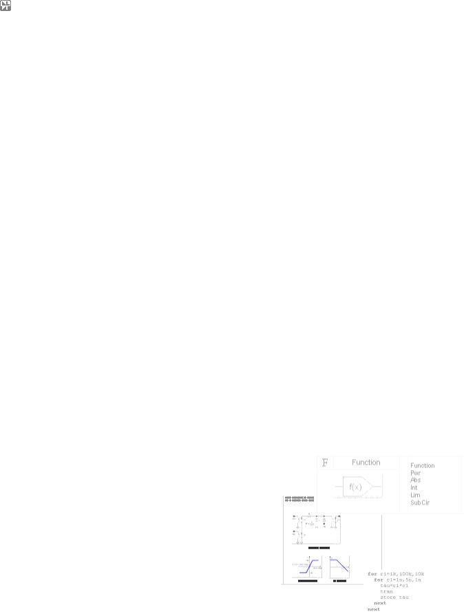
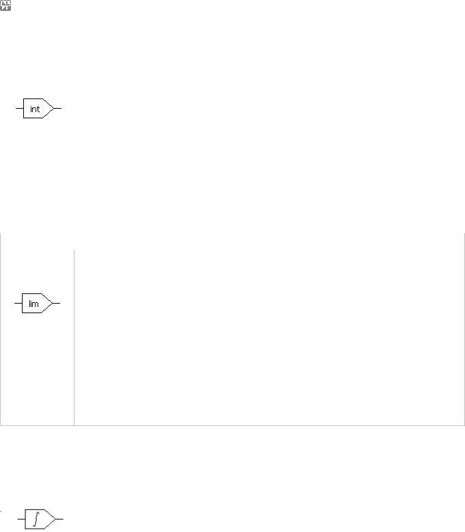
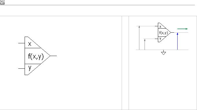
F |
Function |
|
Function |
|
|
|
Pwr |
|
|
Models |
Abs |
|
|
Int |
|
|
|
Lim |
|
|
|
|
Integral |
|
|
|
Table |
|
|
|
SubCir |
|
|
|
|
Руководство Пользователя
|
|
|
|
I |
|
|
|
|
|
Traces |
Vin |
V |
||
|
|
|
||
|
|
|
|
|
P = V • I
326

NL5 circuit simulator |
|
|
Руководство Пользователя |
|
|||
|
|
|
|
|
|
|
|
F |
|
Function |
|
|
|
F/F_Function_Function.nl5 |
|
|
|
|
|
|
|
|
|
|
Model |
Parameter |
Units |
Description |
|
||
|
|
|
|
|
|
|
|
Function |
F(x) |
V |
Output as function of the input. |
|
|||
|
|
|
|
|
|||
F(s) |
|
AC transfer function in s domain. |
|
||||
|
|
|
|
|
|||
|
|
|
|
|
|
|
|
|
|
|
IC |
V |
Initial condition: output voltage. |
|
|
|
|
|
|
|
|
|
|
Arbitrary function.
Transient analysis. F(x) defines output voltage as a function of the following variables:
x – input voltage Vin t - current time
V(name) - voltage on the component name I(name) - current through the component name P(name) – power on the component name
where name is the name of any component in the schematic. If F(x) is blank, output is zero. F(s) is ignored.
Example:
F(x) = x*x
F(x) = x * sin(t)
F(x) = P(r1)+P(r2)
Please note that input voltage x and variables V, I, and P are taken at previous calculation step. This may affect stability of the schematic with closed loop.
AC analysis. F(s) defines transfer function in s domain. Only operators and functions that support complex numbers can be used in this function. The following variables can be used in the function:
f – current AC frequency, Hz
w – angular AC frequency, w = 2πf .
s or p – Laplace parameter, s = p = j*2πf.
z – Z-transform parameter, is defined by custom formula in the Advanced Settings dialog box.
Example:
F(s) = 1/(1+s)
F(s) = exp(-1mk*s)
F(s) is calculated at each frequency. If F(s) is blank, it is assumed to be 1. Also, if F(x) is not blank, it is linearized at DC operating point, and F(s) is multiplied by linearized gain at each frequency.
When calculating DC operating point for transient or AC analysis, output is set to specified output voltage “IC”.
327

NL5 circuit simulator |
|
|
|
Руководство Пользователя |
|
|||
|
|
|
|
|
|
|
|
|
F |
|
Function |
|
|
|
|
F/F_Function_Pwr.nl5 |
|
|
|
|
|
|
|
|
|
|
|
Model |
Parameter |
Units |
|
Description |
|
||
|
|
|
|
|
|
|
|
|
|
Pwr |
power |
|
|
Power. |
|
||
|
|
|
|
|
|
|
||
|
K |
V/V |
|
Gain. |
|
|||
|
|
|
|
|
||||
|
|
|
|
|
|
|
|
|
|
|
|
IC |
V |
|
Initial condition: output voltage. |
|
|
|
|
|
|
|
|
|
||
|
|
|
“Signed” power function. V = K * pwr( Vin, power ). |
|
||||
|
|
|
The function is calculated as follows: |
|
||||
|
|
|
if power = 0: |
|
|
|
|
|
|
|
|
if Vin < 0 . . . : |
V = -K |
|
|||
|
|
|
if Vin = 0 . . . : |
V = 0 |
|
|||
|
|
|
if Vin > 0 . . . : |
V = K |
|
|||
|
|
|
if power ≠ 0: |
|
|
|
|
|
|
|
|
if Vin < 0 . . . : V = - K * (-Vin)power |
|
||||
|
|
|
if Vin = 0 . . . : |
V = 0 |
|
|||
|
|
|
if Vin > 0 . . . : |
V(= K * Vinpower |
|
|||
|
|
|
When calculating DC operating point output is set to specified output voltage “IC”. When |
|
||||
|
|
|
calculating transient, output voltage is always delayed by one calculation step. This may affect |
|
||||
|
|
|
stability of the schematic with closed loop. |
|
||||
|
|
|
|
|
|
|
|
|
|
|
|
|
|
|
|
|
|
F |
|
Function |
|
|
|
|
F/F_Function_Abs.nl5 |
|
|
|
|
|
|
|
|
|
|
|
Model |
Parameter |
Units |
|
Description |
|
||
|
|
|
|
|
|
|
|
|
|
Abs |
K |
V/V |
|
Gain. |
|
||
|
|
|
|
|
|
|
||
|
IC |
V |
|
Initial condition: output voltage. |
|
|||
|
|
|
|
|
||||
|
|
|
|
|
|
|
|
|
Absolute value. V = K * abs( Vin ).
When calculating DC operating point output is set to specified output voltage “IC”. When calculating transient, output voltage is always delayed by one calculation step. This may affect stability of the schematic with closed loop.
328
NL5 circuit simulator |
|
|
Руководство Пользователя |
|
|||
|
|
|
|
|
|
|
|
F |
|
Function |
|
|
|
F/F_Function_Int.nl5 |
|
|
|
|
|
|
|
|
|
|
Model |
Parameter |
Units |
Description |
|
||
|
|
|
|
|
|
|
|
|
Int |
resolution |
V |
Resolution. |
|
||
|
|
|
|
|
|
||
|
K |
V/V |
Gain. |
|
|||
|
|
|
|
||||
|
|
|
|
|
|
|
|
|
|
|
IC |
V |
Initial condition: output voltage. |
|
|
|
|
|
|
|
|
|
|
|
|
|
Rounding function. V = K * round( Vin, resolution ). |
|
|||
|
|
|
Round to the nearest multiple of “resolution”. If resolution = 1, round to the nearest integer. |
|
|||
|
|
|
When calculating DC operating point output is set to specified output voltage “IC”. When |
|
|||
|
|
|
calculating transient, output voltage is always delayed by one calculation step. This may affect |
|
|||
|
|
|
stability of the schematic with closed loop. |
|
|||
|
|
|
|
|
|
|
|
|
|
|
|
|
|
|
|
F |
|
Function |
|
|
|
F/F_Function_Lim.nl5 |
|
|
|
|
|
|
|
|
|
|
Model |
Parameter |
Units |
Description |
|
||
|
|
|
|
|
|
|
|
|
Lim |
Max |
V |
Maximum. |
|
||
|
|
|
|
|
|
||
|
Min |
V |
Minimum. |
|
|||
|
|
|
|
||||
|
|
|
|
|
|
|
|
|
|
|
IC |
V |
Initial condition: output voltage. |
|
|
|
|
|
|
|
|
|
|
Limiting function. The function is calculated as follows:
if Vin < Min . . . : V = Min if Vin > Max . . : V = Max Otherwise . . . . . : V = Vin
When calculating DC operating point output is set to specified output voltage “IC”. When calculating transient, output voltage is always delayed by one calculation step. This may affect stability of the schematic with closed loop.
F |
|
Function |
|
|
|
F/F_Function_Integral.nl5 |
|
|
|
|
|
|
|
|
|
|
Model |
Parameter |
Units |
Description |
|||
|
|
|
|
|
|
||
Integral |
K |
V/V |
Gain. |
||||
|
|
|
|
||||
IC |
V |
Initial condition: output voltage. |
|||||
|
|
|
|||||
|
|
|
Integral. V = K * ∫Vin dt. |
||||
|
|
|
When calculating DC operating point output is set to specified output voltage “IC”. |
||||
|
|
|
|
|
|
|
|
329
NL5 circuit simulator |
|
|
Руководство Пользователя |
|
|||
|
|
|
|
|
|
|
|
F |
|
Function |
|
|
|
F/F_Function_Table.nl5 |
|
|
|
|
|
|
|
|
|
|
Model |
Parameter |
Units |
Description |
|
||
|
|
|
|
|
|
|
|
|
Table |
Table |
|
Comma-separated string, Vin/Vout pairs. |
|
||
|
|
|
|
|
|
||
|
IC |
V |
Initial condition: output voltage. |
|
|||
|
|
|
|
||||
|
|
|
|
|
|
|
|
|
|
|
Look-up table. Function output is defined by “Table” parameter in the csv (“comma |
|
|||
|
|
|
separated values”) format, as follows: |
|
|||
|
|
|
X1,Y1,X2,Y2,…,XN,YN |
|
|||
|
|
|
where Xi,Yi pair defines input value (X) and output value (Y). Output value between specified |
|
|||
|
|
|
points is linearly interpolated. Output value below X1 is linearly extrapolated using X1…X2 |
|
|||
|
|
|
interval data, output value above XN is linearly extrapolated using X(N-1)…XN interval data. |
|
|||
|
|
|
Values X1…XN should be given in an ascending order. |
|
|||
|
|
|
See Working with Table model chapter for more details. |
|
|||
|
|
|
When calculating DC operating point output is set to specified output voltage “IC”. When |
|
|||
|
|
|
calculating transient, output voltage is always delayed by one calculation step. This may affect |
|
|||
|
|
|
stability of the schematic with closed loop. |
|
|||
|
|
|
|
|
|
|
|
|
|
|
|
|
|
|
|
F |
|
Function |
|
|
|
F/F_Function_SubCir.nl5 |
|
|
|
|
|
|
|
|
|
|
Model |
Parameter |
Units |
Description |
|
||
|
|
|
|
|
|
|
|
SubCir |
File |
|
File name of subcircuit schematic. |
|
|||
|
|
|
|
|
|||
Pin1 |
|
Name of subcircuit label connected to pin 1 |
|
||||
|
|
|
|
|
|||
|
|
|
|
|
|
|
|
|
|
|
Pin2 |
|
Name of subcircuit label connected to pin 2 |
|
|
|
|
|
|
|
|
|
|
|
|
|
Cmd |
|
Subcircuit start-up command string |
|
|
|
|
|
|
|
|
|
|
|
|
|
IC |
|
Subcircuit Initial conditions string |
|
|
|
|
|
|
|
|
|
|
Subcircuit. See Working with Subcircuits chapter for details.
330
NL5 circuit simulator
F |
Function-2 |
|
Function |
|
|
|
Mul |
|
|
|
Div |
|
|
|
Sum |
|
|
|
Sub |
|
|
Models |
Max |
|
|
Min |
|
|
|
GT |
|
|
|
|
LT |
|
|
|
Pwr |
|
|
|
Mag |
|
|
|
Phase |
|
|
|
Table |
|
|
|
SubCir |
|
|
|
|
Traces
Руководство Пользователя
I
Vx
V
Vy
P = V • I
331

NL5 circuit simulator |
|
|
Руководство Пользователя |
|
|||
|
|
|
|
|
|
|
|
F |
|
Function-2 |
|
|
F/F_Function-2_Function.nl5 |
|
|
|
|
|
|
|
|
|
|
|
Model |
Parameter |
Units |
Description |
|
||
|
|
|
|
|
|
|
|
Function |
F(x,y) |
V |
Output as function of the inputs. |
|
|||
|
|
|
|
|
|||
F(s) |
|
AC transfer function in s domain. |
|
||||
|
|
|
|
|
|||
|
|
|
|
|
|
|
|
|
|
|
IC |
V |
Initial condition: output voltage. |
|
|
|
|
|
|
|
|
|
|
Arbitrary function.
Transient analysis. F(x,y) defines output voltage as a function of the following variables:
x – input voltage Vx y – input voltage Vy t - current time
V(name) - voltage on the component name I(name) - current through the component name P(name) – power on the component name
where name is the name of any component in the schematic. If F(x,y) is blank, output is zero. F(s) is ignored.
Example:
F(x,y) = sqrt(x*x+y*y)
F(x,y) = x * y * sin(t)
F(x,y) = P(r1)+P(r2)
Please note that input voltages x, y, and variables V, I, P are taken at previous calculation step. This may affect stability of the schematic with closed loop.
AC analysis. F(s) defines transfer function in s domain. Only operators and functions that support complex numbers can be used in this function. The following variables can be used in the function:
f – current AC frequency, Hz
w – angular AC frequency, w = 2πf .
s or p – Laplace parameter, s = p = j*2πf.
z – Z-transform parameter, is defined by custom formula in the Advanced Settings dialog box.
Example:
F(s) = 1/(1+s)
F(s) = exp(-1mk*s)
F(s) is calculated at each frequency. If F(s) is blank, it is assumed to be 1. Also, if F(x,y) is not blank, it is linearized at DC operating point, and F(s) is multiplied by linearized gain..
When calculating DC operating point for transient or AC analysis, output is set to specified output voltage “IC”.
332
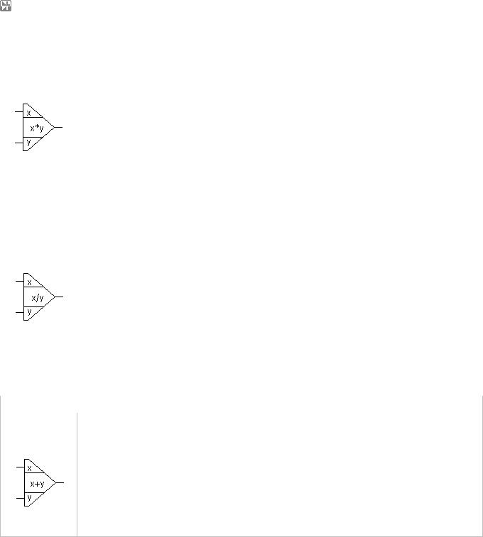
NL5 circuit simulator |
|
|
Руководство Пользователя |
|
|||
|
|
|
|
|
|
|
|
F |
|
Function-2 |
|
|
F/F_Function-2_Mul.nl5 |
|
|
|
|
|
|
|
|
|
|
|
Model |
Parameter |
Units |
Description |
|
||
|
|
|
|
|
|
|
|
|
Mul |
K |
V/V |
Gain. |
|
||
|
|
|
|
|
|
||
|
IC |
V |
Initial condition: output voltage. |
|
|||
|
|
|
|
||||
|
|
|
|
|
|
|
|
|
|
|
Multiplication. V = K * Vx * Vy. |
|
|||
|
|
|
When calculating DC operating point output is set to specified output voltage “IC”. When |
|
|||
|
|
|
calculating transient, output voltage is always delayed by one calculation step. This may affect |
|
|||
|
|
|
stability of the schematic with closed loop. |
|
|||
|
|
|
|
|
|
|
|
|
|
|
|
|
|
|
|
F |
|
Function-2 |
|
|
F/F_Function-2_Div.nl5 |
|
|
|
|
|
|
|
|
|
|
|
Model |
Parameter |
Units |
Description |
|
||
|
|
|
|
|
|
|
|
|
Div |
K |
V/V |
Gain. |
|
||
|
|
|
|
|
|
||
|
IC |
V |
Initial condition: output voltage. |
|
|||
|
|
|
|
||||
|
|
|
|
|
|
|
|
|
|
|
Division. V = K * Vx / Vy. |
|
|||
|
|
|
If Vy = 0, V = 0. |
|
|
|
|
|
|
|
When calculating DC operating point output is set to specified output voltage “IC”. When |
|
|||
|
|
|
calculating transient, output voltage is always delayed by one calculation step. This may affect |
|
|||
|
|
|
stability of the schematic with closed loop. |
|
|||
|
|
|
|
|
|
|
|
|
|
|
|
|
|
|
|
F |
|
Function-2 |
|
|
F/F_Function-2_Sum.nl5 |
|
|
|
|
|
|
|
|
|
|
|
Model |
Parameter |
Units |
Description |
|
||
|
|
|
|
|
|
|
|
|
Sum |
K |
V/V |
Gain. |
|
||
|
|
|
|
|
|
||
|
IC |
V |
Initial condition: output voltage. |
|
|||
|
|
|
|
||||
|
|
|
|
|
|
|
|
Addition. V = K * (Vx + Vy).
When calculating DC operating point output is set to specified output voltage “IC”. When calculating transient, output voltage is always delayed by one calculation step. This may affect stability of the schematic with closed loop.
333
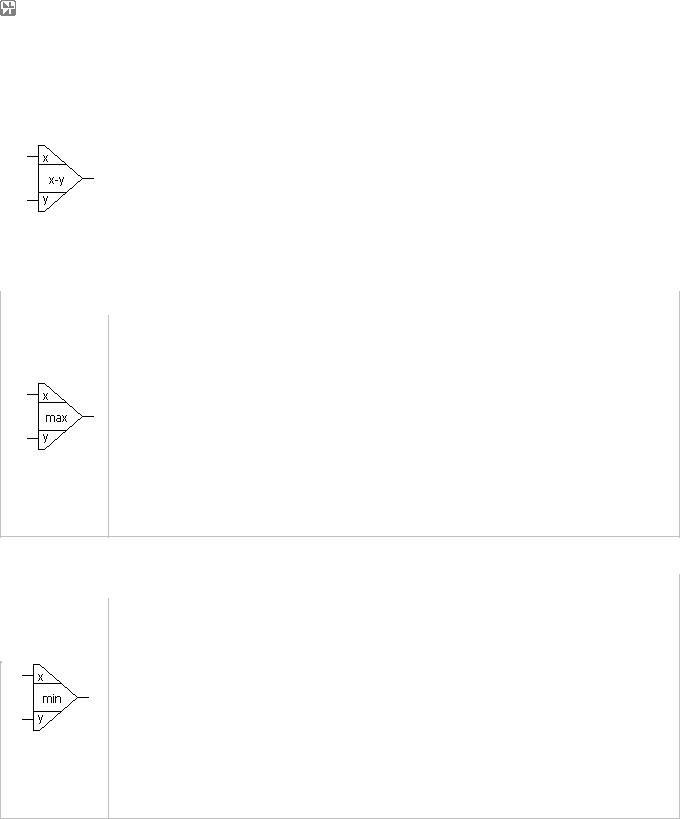
NL5 circuit simulator |
|
|
Руководство Пользователя |
|
|||
|
|
|
|
|
|
|
|
F |
|
Function-2 |
|
|
F/F_Function-2_Sub.nl5 |
|
|
|
|
|
|
|
|
|
|
|
Model |
Parameter |
Units |
Description |
|
||
|
|
|
|
|
|
|
|
|
Sub |
K |
V/V |
Gain. |
|
||
|
|
|
|
|
|
||
|
IC |
V |
Initial condition: output voltage. |
|
|||
|
|
|
|
||||
|
|
|
|
|
|
|
|
|
|
|
Subtraction. V = K * (Vx - Vy). |
|
|||
|
|
|
When calculating DC operating point output is set to specified output voltage “IC”. When |
|
|||
|
|
|
calculating transient, output voltage is always delayed by one calculation step. This may affect |
|
|||
|
|
|
stability of the schematic with closed loop. |
|
|||
|
|
|
|
|
|
|
|
|
|
|
|
|
|
|
|
F |
|
Function-2 |
|
|
F/F_Function-2_Max.nl5 |
|
|
|
|
|
|
|
|
|
|
|
Model |
Parameter |
Units |
Description |
|
||
|
|
|
|
|
|
|
|
|
Max |
K |
V/V |
Gain. |
|
||
|
|
|
|
|
|
||
|
IC |
V |
Initial condition: output voltage. |
|
|||
|
|
|
|
||||
|
|
|
|
|
|
|
|
Maximum. V = K * max( Vx, Vy ).
if Vx >= Vy . . : V = K * Vx if Vx < Vy . . . : V = K * Vy
When calculating DC operating point output is set to specified output voltage “IC”. When calculating transient, output voltage is always delayed by one calculation step. This may affect stability of the schematic with closed loop.
F |
|
Function-2 |
|
|
F/F_Function-2_Min.nl5 |
|
|
|
|
|
|
|
|
|
Model |
Parameter |
Units |
Description |
||
|
|
|
|
|
|
|
|
Min |
K |
V/V |
Gain. |
||
|
|
|
|
|
||
|
IC |
V |
Initial condition: output voltage. |
|||
|
|
|
||||
Minimum. V = K * min(Vx, Vy).
if Vx >= Vy . . : V = K * Vy if Vx < Vy . . . : V = K * Vx
When calculating DC operating point output is set to specified output voltage “IC”. When calculating transient, output voltage is always delayed by one calculation step. This may affect stability of the schematic with closed loop.
334
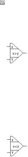
NL5 circuit simulator |
|
|
|
Руководство Пользователя |
|
|||
|
|
|
|
|
|
|
|
|
F |
|
Function-2 |
|
|
|
F/F_Function-2_GT.nl5 |
|
|
|
|
|
|
|
|
|
|
|
|
Model |
Parameter |
Units |
Description |
|
|||
|
|
|
|
|
|
|
|
|
|
GT |
IC |
V |
|
Initial condition: output voltage. |
|
||
|
|
|
|
|
|
|
||
|
Greater than. V = Vx > Vy ? High : Low. |
|
||||||
|
|
|
|
|||||
|
|
|
if Vx <= Vy . . : |
V = Low |
|
|||
|
|
|
if Vx > Vy . . . : |
V = High |
|
|||
|
|
|
High and Low are logical levels. To see and set logical levels go to Transient | Settings, or |
|
||||
|
|
|
AC | Settings then click Advanced button. |
|
||||
|
|
|
When calculating DC operating point output is set to specified output voltage “IC”. When |
|
||||
|
|
|
calculating transient, output voltage is always delayed by one calculation step. This may affect |
|
||||
|
|
|
stability of the schematic with closed loop. |
|
||||
|
|
|
|
|
|
|
|
|
|
|
|
|
|
|
|
|
|
F |
|
Function-2 |
|
|
|
F/F_Function-2_LT.nl5 |
|
|
|
|
|
|
|
|
|
|
|
|
Model |
Parameter |
Units |
Description |
|
|||
|
|
|
|
|
|
|
|
|
|
LT |
IC |
V |
|
Initial condition: output voltage. |
|
||
|
|
|
|
|
|
|
||
|
Less than. V = Vx < Vy ? High : Low. |
|
||||||
|
|
|
|
|||||
|
|
|
if Vx < Vy . . . . : |
V = High |
|
|||
|
|
|
if Vx >= Vy . . . : |
V = Low |
|
|||
|
|
|
High and Low are logical levels. To see and set logical levels go to Transient | Settings, or |
|
||||
|
|
|
AC | Settings then click Advanced button. |
|
||||
|
|
|
When calculating DC operating point output is set to specified output voltage “IC”. When |
|
||||
|
|
|
calculating transient, output voltage is always delayed by one calculation step. This may affect |
|
||||
|
|
|
stability of the schematic with closed loop. |
|
||||
|
|
|
|
|
|
|
|
|
335
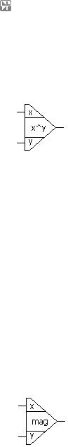
NL5 circuit simulator |
|
|
Руководство Пользователя |
|
|||
|
|
|
|
|
|
|
|
F |
|
Function-2 |
|
|
F/F_Function-2_Pwr.nl5 |
|
|
|
|
|
|
|
|
|
|
|
Model |
Parameter |
Units |
Description |
|
||
|
|
|
|
|
|
|
|
|
Pwr |
K |
V/V |
Gain. |
|
||
|
|
|
|
|
|
||
|
IC |
V |
Initial condition: output voltage. |
|
|||
|
|
|
|
||||
|
|
|
|
|
|
|
|
|
|
|
“Signed” power function. V = K * pwr( Vx, Vy ). |
|
|||
|
|
|
The function is calculated as follows: |
|
|||
|
|
|
if Vy = 0: |
|
|
|
|
|
|
|
if Vx < 0. . . : V = -K |
|
|||
|
|
|
if Vx = 0. . . : V = 0 |
|
|||
|
|
|
if Vx > 0. . . : V = K |
|
|||
|
|
|
if Vy ≠ 0: |
|
|
|
|
|
|
|
if Vx < 0. . . : V = - K * (-Vx)Vy |
|
|||
|
|
|
if Vx = 0. . . : V = 0 |
|
|||
|
|
|
if Vx > 0. . . : V = K * VxVy |
|
|||
|
|
|
When calculating DC operating point output is set to specified output voltage “IC”. When |
|
|||
|
|
|
calculating transient, output voltage is always delayed by one calculation step. This may affect |
|
|||
|
|
|
stability of the schematic with closed loop. |
|
|||
|
|
|
|
|
|
|
|
|
|
|
|
|
|
|
|
F |
|
Function-2 |
|
|
F/F_Function-2_Mag.nl5 |
|
|
|
|
|
|
|
|
|
|
|
Model |
Parameter |
Units |
Description |
|
||
|
|
|
|
|
|
|
|
|
Mag |
K |
V/V |
Gain. |
|
||
|
|
|
|
|
|
||
|
IC |
V |
Initial condition: output voltage. |
|
|||
|
|
|
|
||||
|
|
|
|
|
|
|
|
|
|
|
Magnitude. V = K * sqrt( Vx2 + Vy2 ). |
|
|||
|
|
|
When calculating DC operating point output is set to specified output voltage “IC”. When |
|
|||
|
|
|
calculating transient, output voltage is always delayed by one calculation step. This may affect |
|
|||
|
|
|
stability of the schematic with closed loop. |
|
|||
|
|
|
|
|
|
|
|
336
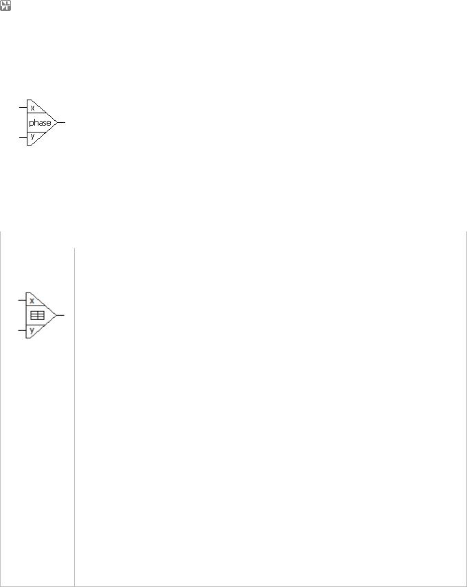
NL5 circuit simulator |
|
|
Руководство Пользователя |
|
|||
|
|
|
|
|
|
|
|
F |
|
Function-2 |
|
|
F/F_Function-2_Phase.nl5 |
|
|
|
|
|
|
|
|
|
|
|
Model |
Parameter |
Units |
Description |
|
||
|
|
|
|
|
|
|
|
Phase |
K |
V/V |
Gain. |
|
|||
|
|
|
|
|
|||
IC |
V |
Initial condition: output voltage. |
|
||||
|
|
|
|
||||
|
|
|
|
|
|
|
|
|
|
|
Phase. V = K * phase( Vx, Vy ). |
|
|||
|
|
|
V in Volts is equal to phase of a vector Vx + jVy in degrees. |
|
|||
|
|
|
If Vx = 0 and Vy = 0: V = 0. |
|
|||
|
|
|
When calculating DC operating point output is set to specified output voltage “IC”. When |
|
|||
|
|
|
calculating transient, output voltage is always delayed by one calculation step. This may affect |
|
|||
|
|
|
stability of the schematic with closed loop. |
|
|||
|
|
|
|
|
|
|
|
|
|
|
|
|
|
|
|
F |
|
Function-2 |
|
|
F/F_Function-2_Table.nl5 |
|
|
|
|
|
|
|
|
|
|
|
Model |
Parameter |
Units |
Description |
|
||
|
|
|
|
|
|
|
|
|
Table |
X |
|
Comma-separated string, X (input values). |
|
||
|
|
|
|
|
|
||
|
Y |
|
Comma-separated string, Y (input values). |
|
|||
|
|
|
|
|
|||
|
|
|
|
|
|
|
|
|
|
|
Table |
|
Comma-separated string, Table of Z (output values). |
|
|
|
|
|
|
|
|
|
|
|
|
|
IC |
V |
Initial condition: output voltage. |
|
|
|
|
|
|
|
|
|
|
2D look-up table. Function output is defined by “Table” parameter in the csv (“comma separated values”) format, as follows:
“Table” parameter of the model defines output of the component Z as a function of X and Y inputs of the component in the following format:
Z11,Z12,…,Z1N,Z21,Z22,…,Z2N,…,ZM1,ZM2,…,ZMN
where:
Zij defines output of the function for input values Xi and Yj;
N is total number of X input values, defined by “X” parameter;
M is total number of Y input values, defined by “Y” parameter.
Output value between specified X and Y points is linearly interpolated on both coordinates.
Output value below X1 is linearly extrapolated using X1…X2 interval data, output value above XN is linearly extrapolated using X(N-1)…XN interval data. The same rule is applied to Y coordinate
See Working with 2D Table model chapter for more details.
When calculating DC operating point output is set to specified output voltage “IC”. When calculating transient, output voltage is always delayed by one calculation step. This may affect stability of the schematic with closed loop.
337

NL5 circuit simulator |
|
|
Руководство Пользователя |
|
|||
|
|
|
|
|
|
|
|
F |
|
Function-2 |
|
|
F/F_Function-2_SubCir.nl5 |
|
|
|
|
|
|
|
|
|
|
|
Model |
Parameter |
Units |
Description |
|
||
|
|
|
|
|
|
|
|
SubCir |
File |
|
File name of subcircuit schematic. |
|
|||
|
|
|
|
|
|||
Pin1 |
|
Name of subcircuit label connected to pin 1 |
|
||||
|
|
|
|
|
|||
|
|
|
|
|
|
|
|
|
|
|
Pin2 |
|
Name of subcircuit label connected to pin 2 |
|
|
|
|
|
|
|
|
|
|
|
|
|
Pin3 |
|
Name of subcircuit label connected to pin 3 |
|
|
|
|
|
|
|
|
|
|
|
|
|
Cmd |
|
Subcircuit start-up command string |
|
|
|
|
|
|
|
|
|
|
|
|
|
IC |
|
Subcircuit Initial conditions string |
|
|
|
|
|
|
|
|
|
|
|
|
|
Subcircuit. See Working with Subcircuits chapter for details. |
|
|||
|
|
|
|
|
|
|
|
338
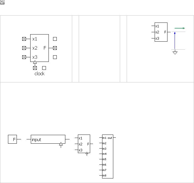
NL5 circuit simulator |
Руководство Пользователя |
F |
Custom function |
Function |
Models |
Traces |
I
V
P = V • I
This is a customized component. A component can be edited in the Edit Component dialog box. See Editing customized component chapter for instructions on editing a component.
This component may have:
-arbitrary size up to 32(width) X 8(height),
-up to 8 inputs on the left side,
-one output on the right side,
-one or no clock pins on the bottom side.
-custom input and output names.
Examples of Custom function component:
339
NL5 circuit simulator |
|
|
Руководство Пользователя |
|
|||
|
|
|
|
|
|
|
|
|
|
|
|
|
|
F/F_Custom_Function_Ex1.nl5 |
|
F |
|
Custom function |
|
|
F/F_Custom_Function_Ex2.nl5 |
|
|
|
|
|
|
|
|
F/F_Custom_Function_Ex3.nl5 |
|
|
|
|
|
|
|
|
|
|
Model |
Parameter |
Units |
Description |
|
||
|
|
|
|
|
|
|
|
Function |
F(x) |
V |
Output as function of the inputs. |
|
|||
|
|
|
|
|
|||
F(s) |
|
AC transfer function in s domain. |
|
||||
|
|
|
|
|
|||
|
|
|
|
|
|
|
|
|
|
|
IC |
V |
Initial condition: output voltage. |
|
|
|
|
|
|
|
|
|
|
Arbitrary function.
Transient analysis. F(x) defines output voltage as a function of the following variables:
pin_name – input voltage on the input pin “pin_name” t - current time
V(name) - voltage on the component name I(name) - current through the component name P(name) – power on the component name
where name is the name of any component in the schematic. If F(x) is blank, output is zero. F(s) is ignored.
Example:
F(x) = max(x1,x2,x3)
F(x) = (in1+in2)*V(R1)
If clock pin does not exist, the model operates in “continuous” mode: the function is calculated and applied to the output on every calculation step. Please note that input voltages and variables V, I, P are taken at previous calculation step. This may affect stability of the schematic with closed loop.
If clock pin exists, the model operates in “synchronized” mode: the function is calculated and applied to the output only on rising edge of logical clock signal. As a result, “synchronized” mode provides faster simulation than “continuous” mode.
AC analysis. F(s) defines transfer function in s domain. Only operators and functions that support complex numbers can be used in this function. The following variables can be used in the function:
f – current AC frequency, Hz
w – angular AC frequency, w = 2πf .
s or p – Laplace parameter, s = p = j*2πf.
z – Z-transform parameter, is defined by custom formula in the Advanced Settings dialog box.
Example:
F(s) = 1/(1+s)
F(s) = exp(-1mk*s)
F(s) is calculated at each frequency. If F(s) is blank, it is assumed to be 1. Also, if F(x) is not blank, it is linearized at DC operating point, and F(s) is multiplied by linearized gain.
When calculating DC operating point for transient or AC analysis, output is set to specified output voltage “IC”.
If clock pin exists, F(s) is ignored, and transfer function of the model is zero.
340
NL5 circuit simulator |
Руководство Пользователя |
I |
Current source |
Models
I
Pulse
Step
Sin
PWL
Function
File
Trace
SubCir
Traces
V

 I
I
P = V • I
I |
|
Current source |
|
|
I/I_CS_I.nl5 |
|
|
|
|
|
|
|
|
|
Model |
Parameter |
Units |
Description |
||
|
|
|
|
|
|
|
|
|
I |
I |
A |
Current. |
|
|
|
|
|
|
|
|
|
|
Constant current source. Current = “I”. |
||||
|
|
|
||||
|
|
|
|
|
|
|
341
NL5 circuit simulator |
|
|
Руководство Пользователя |
|
|||
|
|
|
|
|
|
|
|
I |
|
Current source |
|
|
I/I_CS_Pulse.nl5 |
|
|
|
|
|
|
|
|
|
|
|
Model |
Parameter |
Units |
Description |
|
||
|
|
|
|
|
|
|
|
|
Pulse |
I1 |
A |
Pulse On current. |
|
||
|
|
|
|
|
|
||
|
I0 |
A |
Pulse Off current. |
|
|||
|
|
|
|
||||
|
|
|
|
|
|
|
|
|
|
|
Period |
s |
Period. |
|
|
|
|
|
|
|
|
|
|
|
|
|
Width |
s |
Pulse width. |
|
|
|
|
|
|
|
|
|
|
|
|
|
Slope |
|
Slope type: Linear/Cos/Exp |
|
|
|
|
|
|
|
|
|
|
|
|
|
Rise |
s |
Pulse rise length. |
|
|
|
|
|
|
|
|
|
|
|
|
|
Fall |
s |
Pulse fall length. |
|
|
|
|
|
|
|
|
|
|
|
|
|
Delay |
s |
Delay before first pulse starts. |
|
|
|
|
|
|
|
|
|
|
Pulse current source. Pulses start after “Delay” time. “Rise” time is included into “Width”, “Fall” time is not included into “Width”. Almost every parameter can be set to zero and infinity (“inf”), otherwise the error message will be displayed.
Slope type applies both to pulse rise and fall. The following slope types are available:
Linear |
Cos (cosine) |
Exp (exponential) |
342
NL5 circuit simulator |
|
|
Руководство Пользователя |
|
|||
|
|
|
|
|
|
|
|
I |
|
Current source |
|
|
I/I_CS_Step.nl5 |
|
|
|
|
|
|
|
|
|
|
|
Model |
Parameter |
Units |
Description |
|
|
|
|
|
|
|
|
|
|
|
|
Step |
I1 |
A |
Step On current. |
|
|
|
|
|
|
|
|
|
||
|
I0 |
A |
Step Off current. |
|
|
||
|
|
|
|
|
|||
|
|
|
|
|
|
|
|
|
|
|
Slope |
|
Slope type: Linear/Cos/Exp |
|
|
|
|
|
|
|
|
|
|
|
|
|
Rise |
s |
Step rise length. |
|
|
|
|
|
|
|
|
|
|
|
|
|
Delay |
s |
Delay before step starts. |
|
|
|
|
|
|
|
|
|
|
|
|
|
Step current source. Step starts after “Delay” time. |
|
|||
|
|
|
The following slope types are available: |
|
|
||
|
|
|
Linear |
|
Cos (cosine) |
Exp (exponential) |
|
|
|
|
|
|
|
|
|
343
NL5 circuit simulator |
|
|
|
Руководство Пользователя |
|
|||
|
|
|
|
|
|
|
|
|
I |
|
Current source |
|
|
|
I/I_CS_Sin.nl5 |
|
|
|
|
|
|
|
|
|
|
|
|
Model |
Parameter |
|
Units |
Description |
|
||
|
|
|
|
|
|
|
|
|
|
Sin |
I1 |
|
A |
Current amplitude. |
|
||
|
|
|
|
|
|
|
||
|
I0 |
|
A |
Current baseline. |
|
|||
|
|
|
|
|
||||
|
|
|
|
|
|
|
|
|
|
|
|
Period |
|
s |
Period. |
|
|
|
|
|
|
|
|
|
|
|
|
|
|
Phase |
|
deg |
Phase. |
|
|
|
|
|
|
|
|
|
|
|
|
|
|
Delay |
|
s |
Delay before sine signal starts. |
|
|
|
|
|
|
|
|
|
||
|
|
|
Sine current source. Sine signal starts after “Delay” time. “Phase” is sine phase in degrees at |
|
||||
|
|
|
the moment when signal starts: |
|
||||
|
|
|
|
Phase = 0 |
|
Phase = 90 |
|
|
|
|
|
If transient is paused, sine period changed, then transient is continued, the phase of the signal |
|
||||
|
|
|
remains continuous, providing smooth sine signal of variable frequency: |
|
||||
|
|
|
|
|
|
|
|
|
344
NL5 circuit simulator |
|
|
|
|
Руководство Пользователя |
|
|||
|
|
|
|
|
|
|
|
|
|
I |
|
Current source |
|
|
|
|
I/I_CS_PWL.nl5 |
|
|
|
|
|
|
|
|
|
|
|
|
|
Model |
Parameter |
|
Units |
|
Description |
|
||
|
|
|
|
|
|
|
|
|
|
|
PWL |
pwl |
|
|
|
Comma-separated string. |
|
||
|
|
|
|
|
|
|
|
||
|
Cycle |
|
|
|
Cycling (repeat): No/Yes. |
|
|||
|
|
|
|
|
|
|
|||
|
|
|
|
|
|
|
|
|
|
|
|
|
Delay |
|
s |
|
Delay. |
|
|
|
|
|
|
|
|
|
|||
|
|
|
Piece-wise linear current source. Signal is defined by “pwl” parameter in the csv (“comma- |
|
|||||
|
|
|
separated values”) format, as follows: |
|
|||||
|
|
|
t0,I0,t1,I1,...,tn,In |
|
|
|
|||
|
|
|
where all t and I can be numerical values or expressions. If t<t0, signal is I0. If t0<t<t1, signal |
|
|||||
|
|
|
value is linearly interpolated between I0 and I1, etc. If t>tn, then signal value is In if “Cycle” |
|
|||||
|
|
|
parameter is set to “No”, otherwise signal defined in t0…tn interval is repeated continuously. In |
|
|||||
|
|
|
addition, the whole signal is delayed by “Delay” time. |
|
|||||
|
|
|
Example: |
|
|
|
|
|
|
|
|
|
|
pwl = 0,0,1,2,4,3,5,0,8,0 |
|
||||
|
|
|
If “Cycle” = Yes, “Delay” = 0, the following current will be generated: |
|
|||||
|
|
|
See Working with PWL source chapter for more details. |
|
|||||
|
|
|
|
|
|
|
|
|
|
|
|
|
|
|
|
|
|
|
|
I |
|
Current source |
|
|
|
|
I/I_CS_Function.nl5 |
|
|
|
|
|
|
|
|
|
|
|
|
|
Model |
Parameter |
|
Units |
|
Description |
|
||
|
|
|
|
|
|
|
|
|
|
Function |
F(t) |
|
A |
|
Function |
|
|||
|
|
|
|
|
|
|
|||
Arbitrary function. F(t) defines current as a function of the following variables: |
|
||||||||
|
|
|
|
||||||
|
|
|
t - current time |
|
|
|
|||
|
|
|
V(name) - voltage on the component name |
|
|||||
|
|
|
I(name) - current through the component name |
|
|||||
|
|
|
P(name) – power on the component name |
|
|||||
|
|
|
where name is the name of any component in the schematic. If F(t) is blank, current is zero. |
|
|||||
|
|
|
Example: |
|
|
|
|
|
|
|
|
|
F(t) = sin(t) * (1+cos(t*.01)) |
|
|||||
|
|
|
F(t) = V(R1) * I(R1) |
|
|
|
|||
|
|
|
Please note that V, I, and P variables are taken at previous calculation step. This may affect |
|
|||||
|
|
|
stability of the schematic with closed loop. |
|
|||||
|
|
|
|
|
|
|
|
|
|
345

NL5 circuit simulator |
|
|
Руководство Пользователя |
|
|||
|
|
|
|
|
|
|
|
I |
|
Current source |
|
|
I/I_CS_File.nl5 |
|
|
|
|
|
|
|
|
|
|
|
Model |
Parameter |
Units |
Description |
|
||
|
|
|
|
|
|
|
|
|
File |
File |
|
File name. |
|
||
|
|
|
|
|
|
||
|
Cycle |
|
Cycling (repeat): No/Yes. |
|
|||
|
|
|
|
|
|||
|
|
|
|
|
|
|
|
|
|
|
Delay |
s |
Delay. |
|
|
|
|
|
|
|
|
|
|
Current source defined in the text file.“File“ parameter is a file name, with full path to the file. If the file is located in the same directory as schematic file, the path can be omitted. Signal is defined in the following format:
<if first line does not start with a number, it is ignored> t0,I0
t1,I1
.....
tn,In
where all t and I can be numerical values or expressions. If t<t0, signal is v0. If t0<t<t1, signal value is linearly interpolated between I0 and I1, etc. If t>tn, then signal value is In if “Cycle” parameter is set to “No”, otherwise signal defined in t0…tn interval is repeated continuously. In addition, the whole signal is delayed by “Delay” time.
Example:
0,0
1,2
4,3
5,0
8,0
If “Cycle” = Yes, “Delay” = 0, the following current will be generated:
I |
|
Current source |
|
|
I/I_CS_Trace.nl5 |
|
|
|
|
|
|
|
|
|
Model |
Parameter |
Units |
Description |
||
|
|
|
|
|
|
|
|
Trace |
Trace |
|
Trace name. |
||
|
|
|
|
|
||
|
Cycle |
|
Cycling (repeat): No/Yes. |
|||
|
|
|
|
|||
|
|
|
|
|
|
|
|
|
|
Delay |
s |
Delay. |
|
|
|
|
|
|
|
|
|
|
|
Current source defined by a trace. “Trace” parameter is a name of the trace in the Trace list |
|||
|
|
|
(Transient/Data). Only traces loaded from data file, imported from text or binary file, |
|||
|
|
|
duplicated, or pasted from clipboard can be used for the current source. If “Cycle” parameter |
|||
|
|
|
is set to “Yes”, the signal is repeated continuously. In addition, the whole signal is delayed by |
|||
|
|
|
“Delay” time. |
|
|
|
|
|
|
|
|
|
|
346

NL5 circuit simulator |
|
|
Руководство Пользователя |
|
|||
|
|
|
|
|
|
|
|
I |
|
Current source |
|
|
I/I_CS_SubCir.nl5 |
|
|
|
|
|
|
|
|
|
|
|
Model |
Parameter |
Units |
Description |
|
||
|
|
|
|
|
|
|
|
SubCir |
File |
|
File name of subcircuit schematic. |
|
|||
|
|
|
|
|
|||
Pin1 |
|
Name of subcircuit label connected to pin 1 |
|
||||
|
|
|
|
|
|||
|
|
|
|
|
|
|
|
|
|
|
Pin2 |
|
Name of subcircuit label connected to pin 2 |
|
|
|
|
|
|
|
|
|
|
|
|
|
Cmd |
|
Subcircuit start-up command string |
|
|
|
|
|
|
|
|
|
|
|
|
|
IC |
|
Subcircuit Initial conditions string |
|
|
|
|
|
|
|
|
|
|
|
|
|
Subcircuit. See Working with Subcircuits chapter for details. |
|
|||
|
|
|
|
|
|
|
|
347

NL5 circuit simulator |
Руководство Пользователя |
I |
Voltage controlled |
|
Linear |
current source |
|
||
|
Function |
||
|
|
|
|
|
|
Models |
PWL |
|
|
VCO |
|
|
|
|
|
|
|
|
Pulse |
|
|
|
PWM |
|
|
|
SubCir |
|
|
|
|
Views
Traces
V in |
V I |
|||
|
|
|
|
|
P = V • I |
|
|
||
I |
|
Voltage controlled current source |
|
I/I_VCCS_Linear.nl5 |
||
|
|
|
|
|
|
|
|
Model |
Parameter |
Units |
Description |
||
|
|
|
|
|
|
|
|
Linear |
K |
A/V |
Gain |
||
|
|
|
|
|
||
|
|
|
|
|
||
Linear voltage controlled current source. I = K * Vin.
348

NL5 circuit simulator |
|
|
Руководство Пользователя |
|
|||
|
|
|
|
|
|
|
|
I |
|
Voltage controlled current source |
|
I/I_VCCS_Function.nl5 |
|
||
|
|
|
|
|
|
|
|
|
Model |
Parameter |
Units |
Description |
|
||
|
|
|
|
|
|
|
|
Function |
F(x) |
A |
Output as function of the input. |
|
|||
|
|
|
|
|
|||
F(s) |
|
AC transfer function in s domain. |
|
||||
|
|
|
|
|
|||
|
|
|
|
|
|
|
|
|
|
|
IC |
A |
Initial condition: output current. |
|
|
|
|
|
|
|
|
|
|
Arbitrary function.
Transient analysis. F(x) defines output current as a function of the following variables:
x – input voltage Vin t - current time
V(name) - voltage on the component name I(name) - current through the component name P(name) – power on the component name
where name is the name of any component in the schematic. If F(x) is blank, output is zero. F(s) is ignored.
Example:
F(x) = x*x
F(x) = x * sin(t)
F(x) = P(r1)+P(r2)
Please note that input voltage x and variables V, I, and P are taken at previous calculation step. This may affect stability of the schematic with closed loop.
AC analysis. F(s) defines transfer function in s domain. Only operators and functions that support complex numbers can be used in this function. The following variables can be used in the function:
f – current AC frequency, Hz
w – angular AC frequency, w = 2πf .
s or p – Laplace parameter, s = p = j*2πf.
z – Z-transform parameter, is defined by custom formula in the Advanced Settings dialog box.
Example:
F(s) = 1/(1+s)
F(s) = exp(-1mk*s)
F(s) is calculated at each frequency. If F(s) is blank, it is assumed to be 1. Also, if F(x) is not blank, it is linearized at DC operating point, and F(s) is multiplied by linearized gain.
When calculating DC operating point for transient or AC analysis, output is set to specified output current “IC”.
349
NL5 circuit simulator |
|
|
|
Руководство Пользователя |
|
|||
|
|
|
|
|
|
|
|
|
I |
|
Voltage controlled current source |
|
I/I_VCCS_PWL.nl5 |
|
|||
|
|
|
|
|
|
|
|
|
|
Model |
Parameter |
Units |
|
Description |
|
||
|
|
|
|
|
|
|
|
|
|
PWL |
pwl |
|
|
Comma-separated string, K(Vin) |
|
||
|
|
|
|
|
|
|
||
|
Piece-wise linear voltage controlled current source. Source gain K is defined by “pwl” |
|
||||||
|
|
|
|
|||||
|
|
|
string as a function of input voltage Vin. See Working with PWL model chapter for details. |
|
||||
|
|
|
|
|
|
|
|
|
|
|
|
|
|
|
|||
I |
|
Voltage controlled current source |
|
I/I_VCCS_VCO.nl5 |
|
|||
|
|
|
|
|
|
|
|
|
|
Model |
Parameter |
Units |
|
Description |
|
||
|
|
|
|
|
|
|
|
|
|
VCO |
I1 |
A |
|
Current amplitude (Sin), or Pulse On current (Pulse). |
|
||
|
|
|
|
|
|
|
||
|
I0 |
A |
|
Current baseline (Sin), or Pulse Off current (Pulse). |
|
|||
|
|
|
|
|
||||
|
|
|
|
|
|
|
|
|
|
|
|
dFdV |
Hz/V |
|
Gain. |
|
|
|
|
|
|
|
|
|
|
|
|
|
|
Phase |
deg |
|
Phase. |
|
|
|
|
|
|
|
|
|
|
|
|
|
|
Type |
|
|
Signal type: Sin/Square/Triangle/Sawtooth. |
|
|
|
|
|
|
|
|
|
||
|
|
|
Voltage controlled oscillator. Output current is a signal with frequency equal to: |
|
||||
|
|
|
f(Hz) = dFdV * Vin. |
|
|
|
||
|
|
|
For Sine signal, “I0” is baseline, and “I1” is amplitude. For Square, Triangle, and Sawtooth |
|
||||
|
|
|
signals, “I0” is Off level, “I1” is On level. “Phase” is additional phase of the signal, in degrees. |
|
||||
|
|
|
|
|
|
|
||
|
|
|
|
|
|
|||
I |
|
Voltage controlled current source |
|
I/I_VCCS_Pulse.nl5 |
|
|||
|
|
|
|
|
|
|
|
|
|
Model |
Parameter |
Units |
|
Description |
|
||
|
|
|
|
|
|
|
|
|
|
Pulse |
Width |
s |
|
Pulse width. |
|
||
|
|
|
|
|
|
|
||
|
Threshold |
V |
|
Voltage threshold. |
|
|||
|
|
|
|
|
||||
|
|
|
|
|
|
|
|
|
|
|
|
I1 |
A |
|
Pulse On current. |
|
|
|
|
|
|
|
|
|
|
|
|
|
|
I0 |
A |
|
Pulse Off current. |
|
|
|
|
|
|
|
|
|
|
|
One-shot pulse generator. When increasing input voltage Vin crosses “Threshold” value, current pulse of “Width” duration is generated. “I0” is pulse Off level, “I1” is pulse On level. If increasing Vin crosses “Threshold” value while pulse is generated, the pulse is restarted.
350

NL5 circuit simulator |
|
|
Руководство Пользователя |
|
|||
|
|
|
|
|
|
|
|
I |
|
Voltage controlled current source |
|
I/I_VCCS_PWM.nl5 |
|
||
|
|
|
|
|
|
|
|
|
Model |
Parameter |
Units |
Description |
|
||
|
|
|
|
|
|
|
|
|
PWM |
I1 |
A |
Pulse On current. |
|
||
|
|
|
|
|
|
||
|
I0 |
A |
Pulse Off current. |
|
|||
|
|
|
|
||||
|
|
|
|
|
|
|
|
|
|
|
F |
Hz |
Frequency. |
|
|
|
|
|
|
|
|
|
|
|
|
|
Phase |
deg |
Phase. |
|
|
|
|
|
|
|
|
|
|
|
|
|
Vmax |
V |
Input voltage corresponding to 100% duty. |
|
|
|
|
|
|
|
|
|
|
|
|
|
Voltage controlled Pulse-Width Modulator. Output current is a pulse signal of frequency “F” |
|
|||
|
|
|
shifted by “Phase”. Input voltage Vin is sampled at the beginning of each cycle of the signal, |
|
|||
|
|
|
and width of the output pulse during this cycle is calculated according to the equation: |
|
|||
|
|
|
width = 1/F * (Vin / Vmax) |
|
|||
|
|
|
or |
|
|
|
|
|
|
|
duty = 100% * (Vin / Vmax); |
|
|||
|
|
|
If the width is equal or less than zero, a short “On” pulse with the width equal to the minimum |
|
|||
|
|
|
calculation step at that moment will be generated. If the width is equal or greater than period |
|
|||
|
|
|
of frequency “F”, a short “Off” pulse at the end of the period will be generated. Due to that, the |
|
|||
|
|
|
frequency of the output signal is always “F". |
|
|||
|
|
|
|
|
|
|
|
|
|
|
|
|
|
||
I |
|
Voltage controlled current source |
|
I/I_VCCS_SubCir.nl5 |
|
||
|
|
|
|
|
|
|
|
|
Model |
Parameter |
Units |
Description |
|
||
|
|
|
|
|
|
|
|
SubCir |
File |
|
File name of subcircuit schematic. |
|
|||
|
|
|
|
|
|||
Pin1 |
|
Name of subcircuit label connected to pin 1 |
|
||||
|
|
|
|
|
|||
|
|
|
|
|
|
|
|
|
|
|
Pin2 |
|
Name of subcircuit label connected to pin 2 |
|
|
|
|
|
|
|
|
|
|
|
|
|
Pin3 |
|
Name of subcircuit label connected to pin 3 |
|
|
|
|
|
|
|
|
|
|
|
|
|
Pin4 |
|
Name of subcircuit label connected to pin 4 |
|
|
|
|
|
|
|
|
|
|
|
|
|
Cmd |
|
Subcircuit start-up command string |
|
|
|
|
|
|
|
|
|
|
|
|
|
IC |
|
Subcircuit Initial conditions string |
|
|
|
|
|
|
|
|
|
|
|
|
|
Subcircuit. See Working with Subcircuits chapter for details. |
|
|||
|
|
|
|
|
|
|
|
351
NL5 circuit simulator |
Руководство Пользователя |
I |
Current controlled |
|
Linear |
current source |
|
||
|
Function |
||
|
|
|
|
|
|
Models |
PWL |
|
|
CCO |
|
|
|
|
|
|
|
|
Pulse |
|
|
|
PWM |
|
|
|
SubCir |
|
|
|
|
Views
Traces
I in |
V I |
|
P = V • I |
|
|
|
|
|
I |
|
Current controlled current source |
|
I/I_CCCS_Linear.nl5 |
||
|
|
|
|
|
|
|
|
Model |
Parameter |
Units |
Description |
||
|
|
|
|
|
|
|
|
Linear |
K |
A/A |
Gain |
||
|
|
|
|
|
||
|
|
|
|
|
||
Linear current controlled current source. I = K * Iin.
352

NL5 circuit simulator |
|
|
Руководство Пользователя |
|
|||
|
|
|
|
|
|
|
|
I |
|
Current controlled current source |
|
I/I_CCCS_Function.nl5 |
|
||
|
|
|
|
|
|
|
|
|
Model |
Parameter |
Units |
Description |
|
||
|
|
|
|
|
|
|
|
Function |
F(x) |
A |
Output as function of the input. |
|
|||
|
|
|
|
|
|||
F(s) |
|
AC transfer function in s domain. |
|
||||
|
|
|
|
|
|||
|
|
|
|
|
|
|
|
|
|
|
IC |
A |
Initial condition: output current. |
|
|
|
|
|
|
|
|
|
|
Arbitrary function.
Transient analysis. F(x) defines output current as a function of the following variables:
x – input current Iin t - current time
V(name) - voltage on the component name I(name) - current through the component name P(name) – power on the component name
where name is the name of any component in the schematic. If F(x) is blank, output is zero. F(s) is ignored.
Example:
F(x) = x*x
F(x) = x * sin(t)
F(x) = P(r1)+P(r2)
Please note that input current x, and variables V, I, and P are taken at previous calculation step. This may affect stability of the schematic with closed loop.
AC analysis. F(s) defines transfer function in s domain. Only operators and functions that support complex numbers can be used in this function. The following variables can be used in the function:
f – current AC frequency, Hz
w – angular AC frequency, w = 2πf .
s or p – Laplace parameter, s = p = j*2πf.
z – Z-transform parameter, is defined by custom formula in the Advanced Settings dialog box.
Example:
F(s) = 1/(1+s)
F(s) = exp(-1mk*s)
F(s) is calculated at each frequency. If F(s) is blank, it is assumed to be 1. Also, if F(x) is not blank, it is linearized at DC operating point, and F(s) is multiplied by linearized gain.
When calculating DC operating point for transient or AC analysis, output is set to specified output current “IC”.
353

NL5 circuit simulator |
|
|
Руководство Пользователя |
|
|||
|
|
|
|
|
|
|
|
I |
|
Current controlled current source |
|
I/I_CCCS_PWL.nl5 |
|||
|
|
|
|
|
|
|
|
|
Model |
Parameter |
Units |
Description |
|||
|
|
|
|
|
|||
|
PWL |
pwl |
|
Comma-separated string, K(Iin) |
|||
|
|
|
Piece-wise linear current controlled current source. Source gain K is defined by “pwl” |
||||
|
|
|
string as a function of input current Iin. See Working with PWLmodel chapter for details. |
||||
|
|
|
|
|
|
|
|
|
|
|
|
|
|||
I |
|
Current controlled current source |
|
I/I_CCCS_CCO.nl5 |
|||
|
|
|
|
|
|
|
|
|
Model |
Parameter |
Units |
Description |
|||
|
|
|
|
|
|
||
|
CCO |
I1 |
A |
Current amplitude (Sin), or Pulse On current (Pulse). |
|||
|
|
|
|
|
|
||
|
I0 |
A |
Current baseline (Sin), or Pulse Off current (Pulse). |
||||
|
|
|
|||||
|
|
|
|
|
|
||
|
|
|
dFdI |
Hz/A |
Gain. |
||
|
|
|
|
|
|
||
|
|
|
Phase |
deg |
Phase. |
||
|
|
|
|
|
|
||
|
|
|
Type |
|
Signal type: Sin/Square/Triangle/Sawtooth. |
||
|
|
|
|
|
|
||
|
|
|
Current controlled oscillator. Output current is a signal with frequency equal to: |
||||
|
|
|
f(Hz) = dFdI * Iin. |
|
|
|
|
|
|
|
For Sine signal, “I0” is baseline, and “I1” is amplitude. For Square, Triangle, and Sawtooth |
||||
|
|
|
signals, “I0” is Off level, “I1” is On level. “Phase” is additional phase of the signal, in degrees. |
||||
|
|
|
|
|
|
||
|
|
|
|
|
|||
I |
|
Current controlled current source |
|
I/I_CCCS_Pulse.nl5 |
|||
|
|
|
|
|
|
|
|
|
Model |
Parameter |
Units |
Description |
|||
|
|
|
|
|
|
||
|
Pulse |
Width |
s |
Pulse width. |
|||
|
|
|
|
|
|
||
|
Threshold |
A |
Current threshold. |
||||
|
|
|
|||||
|
|
|
|
|
|
||
|
|
|
I1 |
A |
Pulse Off current.. |
||
|
|
|
|
|
|
||
|
|
|
I0 |
A |
Phase. |
||
|
|
|
|
|
|
|
|
One-shot pulse generator. When increasing input current Iin crosses “Threshold” value, current pulse of “Width” duration is generated. “I0” is pulse Off level, “I1” is pulse On level. If increasing Iin crosses “Threshold” value while pulse is generated, the pulse is restarted.
354

NL5 circuit simulator |
|
|
Руководство Пользователя |
|
|||
|
|
|
|
|
|
|
|
I |
|
Current controlled current source |
|
I/I_CCCS_PWM.nl5 |
|
||
|
|
|
|
|
|
|
|
|
Model |
Parameter |
Units |
Description |
|
||
|
|
|
|
|
|
|
|
|
PWM |
I1 |
A |
Pulse On current. |
|
||
|
|
|
|
|
|
||
|
I0 |
A |
Pulse Off current. |
|
|||
|
|
|
|
||||
|
|
|
|
|
|
|
|
|
|
|
F |
Hz |
Frequency. |
|
|
|
|
|
|
|
|
|
|
|
|
|
Phase |
deg |
Phase. |
|
|
|
|
|
|
|
|
|
|
|
|
|
Imax |
A |
Input current corresponding to 100% duty. |
|
|
|
|
|
|
|
|
|
|
|
|
|
Current controlled Pulse-Width Modulator. Output current is a pulse signal of frequency “F” |
|
|||
|
|
|
shifted by “Phase”. Input current Iin is sampled at the beginning of each cycle of the signal, |
|
|||
|
|
|
and width of the output pulse during this cycle is calculated according to the equation: |
|
|||
|
|
|
width = 1/F * (Iin / Imax) |
|
|||
|
|
|
or |
|
|
|
|
|
|
|
duty = 100% * (Iin / Imax); |
|
|||
|
|
|
If the width is equal or less than zero, a short “On” pulse with the width equal to the minimum |
|
|||
|
|
|
calculation step at that moment will be generated. If the width is equal or greater than period |
|
|||
|
|
|
of frequency “F”, a short “Off” pulse at the end of the period will be generated. Due to that, the |
|
|||
|
|
|
frequency of the output signal is always “F". |
|
|||
|
|
|
|
|
|
|
|
|
|
|
|
|
|
||
I |
|
Current controlled current source |
|
I/I_CCCS_SubCir.nl5 |
|
||
|
|
|
|
|
|
|
|
|
Model |
Parameter |
Units |
Description |
|
||
|
|
|
|
|
|
|
|
SubCir |
File |
|
File name of subcircuit schematic. |
|
|||
|
|
|
|
|
|||
Pin1 |
|
Name of subcircuit label connected to pin 1 |
|
||||
|
|
|
|
|
|||
|
|
|
|
|
|
|
|
|
|
|
Pin2 |
|
Name of subcircuit label connected to pin 2 |
|
|
|
|
|
|
|
|
|
|
|
|
|
Pin3 |
|
Name of subcircuit label connected to pin 3 |
|
|
|
|
|
|
|
|
|
|
|
|
|
Pin4 |
|
Name of subcircuit label connected to pin 4 |
|
|
|
|
|
|
|
|
|
|
|
|
|
Cmd |
|
Subcircuit start-up command string |
|
|
|
|
|
|
|
|
|
|
|
|
|
IC |
|
Subcircuit Initial conditions string |
|
|
|
|
|
|
|
|
|
|
|
|
|
Subcircuit. See Working with Subcircuits chapter for details. |
|
|||
|
|
|
|
|
|
|
|
355
NL5 circuit simulator |
Руководство Пользователя |
L
Inductor
Models
L
PWL
Function
SubCir
Traces
V  I
I
P = V • I
L |
|
Inductor |
|
|
|
L/L_Inductor_L.nl5 |
|
|
|
|
|
|
|
|
Model |
Parameter |
Units |
Description |
||
|
|
|
|
|
|
|
|
|
L |
L |
H |
Inductance |
|
|
|
|
|
|
|
|
|
|
IC |
A |
Initial condition: current. Leave blank if IC not defined. |
||
|
|
|
||||
|
|
|
|
|
|
|
|
|
|
Linear inductor. V = L*dI/dt. |
|||
|
|
|
When calculating DC operating point, if “IC” is defined, inductor is replaced with current source |
|||
|
|
|
equal to IC. If “IC” is not defined (blank), inductor is temporarily replaced by short circuit, DC |
|||
|
|
|
operating point calculated, and then the current through short circuit is assigned to the |
|||
|
|
|
inductor as its initial current. |
|||
|
|
|
|
|
|
|
|
|
|
|
|
|
|
L |
|
Inductor |
|
|
|
L/L_Inductor_PWL.nl5 |
|
|
|
|
|
|
|
|
Model |
Parameter |
Units |
Description |
||
|
|
|
|
|
|
|
|
PWL |
pwl |
|
Comma-separated string, L(I) |
||
|
|
|
|
|
||
|
IC |
A |
Initial condition: current. Leave blank if IC not defined. |
|||
|
|
|
||||
|
|
|
|
|
|
|
Piece-wise linear capacitor. “pwl” string defines inductance as a function of current. See
Working with PWL model chapter for details.
When calculating DC operating point, if “IC” is defined, inductor is replaced with current source equal to IC. If “IC” is not defined (blank), inductor is temporarily replaced by short circuit, DC operating point calculated, and then the current through short circuit is assigned to the inductor as its initial current.
356

NL5 circuit simulator |
|
|
|
Руководство Пользователя |
|
|||
|
|
|
|
|
|
|
|
|
L |
|
Inductor |
|
|
|
|
L/L_Inductor_Function.nl5 |
|
|
|
|
|
|
|
|
|
|
|
Model |
Parameter |
Units |
Description |
|
|||
|
|
|
|
|
|
|
||
Function |
Z(s) |
Ohm |
Impedance as a function of s parameter. |
|
||||
|
|
|
|
|
|
|||
Impedance function in s domain. For transient, constant impedance Z(0) is used. For |
|
|||||||
|
|
|
|
|||||
|
|
|
linearized AC analysis, complex impedance Z(s) is used. The following variables can be used |
|
||||
|
|
|
in the function: |
|
|
|
|
|
|
|
|
f – current AC frequency, Hz |
|
||||
|
|
|
w – angular AC frequency, |
w = 2πf . |
|
|||
|
|
|
s or p – Laplace parameter, s = p = j*2πf. |
|
||||
|
|
|
z – Z-transform parameter, is defined by custom formula in the Advanced Settings |
|
||||
|
|
|
dialog box. |
|
|
|
|
|
|
|
|
Example: |
|
|
|
|
|
|
|
|
Z(s) = 3n*s + 0.5 |
|
- 3 nH inductor in series with 0.5 Ohm resistor. |
|
||
|
|
|
Z(s) = (1u*s)||(1.0/10p/s) |
- 1 mkH inductor in parallel with 10 pF capacitor. |
|
|||
|
|
|
|
|
|
|
|
|
|
|
|
|
|
|
|
|
|
L |
|
Inductor |
|
|
|
|
L/L_Inductor_SubCir.nl5 |
|
|
|
|
|
|
|
|
|
|
|
Model |
Parameter |
Units |
Description |
|
|||
|
|
|
|
|
|
|
||
SubCir |
File |
|
File name of subcircuit schematic. |
|
||||
|
|
|
|
|
|
|||
Pin1 |
|
Name of subcircuit label connected to pin 1 |
|
|||||
|
|
|
|
|
||||
|
|
|
|
|
|
|
||
|
|
|
Pin2 |
|
Name of subcircuit label connected to pin 2 |
|
||
|
|
|
|
|
|
|
||
|
|
|
Cmd |
|
Subcircuit start-up command string |
|
||
|
|
|
|
|
|
|
||
|
|
|
IC |
|
Subcircuit Initial conditions string |
|
||
|
|
|
|
|
|
|
||
|
|
|
Subcircuit. See Working with Subcircuits chapter for details. |
|
||||
|
|
|
|
|
|
|
|
|
357
NL5 circuit simulator |
Руководство Пользователя |
L |
Voltage controlled |
|
PWL |
|
inductor |
|
|
||
|
|
|
||
|
|
Models |
|
Traces |
|
|
|
|
|
Views
V in |
V I |
|||
|
|
|
|
|
P = V • I |
|
|
||
L |
|
Voltage controlled inductor |
|
L/L_VCL_PWL.nl5 |
||
|
|
|
|
|
|
|
|
Model |
Parameter |
Units |
Description |
||
|
|
|
|
|
|
|
|
PWL |
pwl |
|
Comma-separated string, L(Vin) |
||
|
|
|
|
|
||
|
IC |
A |
Initial condition: current. Leave blank if IC not defined. |
|||
|
|
|
||||
|
|
|
|
|
|
|
Piece-wise linear voltage controlled inductor. At any moment, inductor is a linear inductor. Its inductance L is a function of control voltage:
V = L(Vin)*dI/dt.
“pwl” string defines inductance as a function of control voltage Vin. See Working with PWL model chapter for details.
When calculating DC operating point, if “IC” is defined, inductor is replaced with current source equal to IC. If “IC” is not defined (blank), inductor is temporarily replaced by short circuit, DC operating point calculated, and then the current through short circuit is assigned to the inductor as its initial current.
358
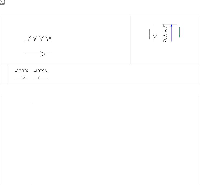
NL5 circuit simulator |
Руководство Пользователя |
L |
Current controlled |
|
PWL |
|
inductor |
|
|
||
|
|
|
||
|
|
Models |
|
Traces |
|
|
|
|
|
Views
I in |
V I |
|
P = V • I |
|
|
|
|
|
L |
|
Current controlled inductor |
|
L/L_CCL_PWL.nl5 |
||
|
|
|
|
|
|
|
|
Model |
Parameter |
Units |
Description |
||
|
|
|
|
|
|
|
|
PWL |
pwl |
|
Comma-separated string, L(Iin) |
||
|
|
|
|
|
||
|
IC |
A |
Initial condition: current. Leave blank if IC not defined. |
|||
|
|
|
||||
|
|
|
|
|
|
|
Piece-wise linear current controlled inductor. At any moment, inductor is a linear inductor. Its inductance L is a function of control current:
V = L(Iin)*dI/dt.
“pwl” string defines inductance as a function of control current Iin. See Working with PWL model chapter for details.
When calculating DC operating point, if “IC” is defined, inductor is replaced with current source equal to IC. If “IC” is not defined (blank), inductor is temporarily replaced by short circuit, DC operating point calculated, and then the current through short circuit is assigned to the inductor as its initial current.
359
NL5 circuit simulator |
Руководство Пользователя |
L |
Coupled |
|
L |
inductors |
|
||
|
|
|
|
|
|
Models |
|
|
|
|
|
Views
Traces
|
I1 |
|
I2 |
||
|
|
|
|
|
|
V1 |
|
V2 |
|||
|
|
|
|
|
|
L |
|
Coupled inductors |
|
|
L/L_CoupledInductors_L.nl5 |
|
|
|
|
|
|
|
|
|
Model |
Parameter |
Units |
Description |
||
|
|
|
|
|
|
|
|
|
L |
L1 |
H |
L1 inductance |
|
|
|
|
|
|
|
|
|
|
L2 |
H |
L2 inductance |
||
|
|
|
||||
|
|
|
|
|
|
|
|
|
|
K |
|
Coupling coefficient (-1…1) |
|
|
|
|
|
|
|
|
|
|
|
IC1 |
A |
L1 initial condition: current. Leave blank if IC1 not defined. |
|
|
|
|
|
|
|
|
|
|
|
IC2 |
A |
L2 initial condition: current. Leave blank if IC2 not defined. |
|
|
|
|
|
|
|
|
Coupled linear inductors.
V1 = L1*dI1/dt + M*dI2/dt
V2 = M*dI1/dt + L2*dI2/dt
Where M = K*sqrt(L1*L2) is mutual inductance.
When calculating DC operating point, initial conditions IC1 and IC2 are independently applied to corresponding inductors L1 and L2, similar to how it is done for the component L (inductor).
360

NL5 circuit simulator |
Руководство Пользователя |
L |
Custom coupled |
|
inductors |
||
|
Models
L
SubCir
IC
Traces
This is a customized component. A component can be edited in the Edit Component dialog box. See Editing customized component chapter for instructions on editing a component.
This component may have:
-height from 2 to 32,
-up to 9 windings (total) on both sides,
-arbitrary length of a winding.
Examples of Custom coupled inductors component:
Views
361

NL5 circuit simulator |
|
|
Руководство Пользователя |
|
|||
|
|
|
|
|
|
|
|
L |
|
Custom coupled inductors |
|
L/L_CustomCoupledInductors_L.nl5 |
|
||
|
|
|
|
|
|
|
|
|
Model |
Parameter |
Units |
Description |
|
||
|
|
|
|
|
|
|
|
|
|
L |
L1 |
H |
L1 inductance |
|
|
|
|
|
|
|
|
|
|
|
|
… |
H |
… |
|
||
|
|
|
|
||||
|
|
|
LN |
H |
LN inductance |
|
|
|
|
|
|
|
|
|
|
|
|
|
K12 |
|
L1-L2 coupling coefficient (-1…1) |
|
|
|
|
|
|
|
|
|
|
|
|
|
… |
|
… |
|
|
|
|
|
K(N-1)N |
|
L(N-1)-LN coupling coefficient (-1…1) |
|
|
|
|
|
|
|
|
|
|
|
|
|
IC1 |
A |
L1 initial condition: current. Leave blank if IC1 not defined. |
|
|
|
|
|
|
|
|
|
|
|
|
|
… |
A |
… |
|
|
|
|
|
ICN |
A |
LN initial condition: current. Leave blank if ICN not defined. |
|
|
|
|
|
|
|
|
|
|
Custom coupled inductors.
V1 = L1*dI1/dt + M12*dI2/dt + … + M1N*dIN/dt
V2 = M12*dI1/dt + L2*dI2/dt + … + M2N*dIN/dt
…
VN = M1N*dI1/dt + M2N*dI2/dt + … + LN*dIN/dt
Where Mij = Kij*sqrt(Li*Lj) is mutual inductance, Mij = Mji.
When calculating DC operating point, initial conditions ICN are independently applied to corresponding inductors LN, similar to how it is done for the component L (inductor).
If only one winding is defined, a component behaves exactly as a linear inductor L.
Please be aware that coupling coefficients Kij should be properly specified within allowable range (-1…1) in order to represent a “physically-realizable” system. See NL5 website
(http://nl5.sidelinesoft.com) and other public resources for more details.
If all coupling coefficients are equal to 1 (or -1), using Winding components W with one magnetizing inductor will give better performance and more stable solution.
L |
|
Custom coupled inductors |
|
L/L_CustomCoupledInductors_SubCir.nl5 |
||
|
|
|
|
|
|
|
|
Model |
Parameter |
Units |
Description |
||
|
|
|
|
|
|
|
SubCir |
File |
|
File name of subcircuit schematic. |
|||
|
|
|
|
|||
Pin1 |
|
Name of subcircuit label connected to pin 1 |
||||
|
|
|
|
|||
|
|
|
|
|
|
|
|
|
|
… |
|
… |
|
|
|
|
PinN |
|
Name of subcircuit label connected to pin N |
|
|
|
|
|
|
|
|
|
|
|
Cmd |
|
Subcircuit start-up command string |
|
|
|
|
|
|
|
|
|
|
|
IC |
|
Subcircuit Initial conditions string |
|
|
|
|
|
|
|
|
Subcircuit. See Working with Subcircuits chapter for details.
362
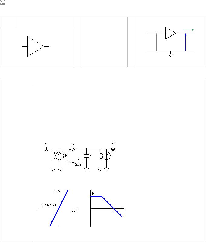
NL5 circuit simulator |
Руководство Пользователя |
O
Amplifier
Models
Linear
OpAmp
Comparator
Function
PWL
SubCir
Traces
I
Vin |
V |
|
P = V • I
O |
|
Amplifier |
|
|
|
O/O_Amplifier_Linear.nl5 |
|
|
|
|
|
|
|
|
|
|
Model |
Parameter |
Units |
Description |
|||
|
|
|
|
|
|
||
Linear |
K |
V/V |
Gain |
||||
|
|
|
|
||||
f1 |
Hz |
Unit gain frequency. |
|||||
|
|
|
|||||
|
|
|
|
|
|
||
|
|
|
IC |
V |
Initial condition: output voltage. |
||
|
|
|
|
|
|
|
|
Linear amplifier. “K” is open loop gain. Frequency response consists of one pole, “f1” is unit gain frequency. “K” and “f1” can be set to infinity (“inf”).
When calculating DC operating point, if “f1” is not infinity and “IC” is defined, amplifier output is set to specified output voltage “IC”. If “IC” is blank, static characteristic is used.
Equivalent schematic
Static characteristic |
AC response |
363
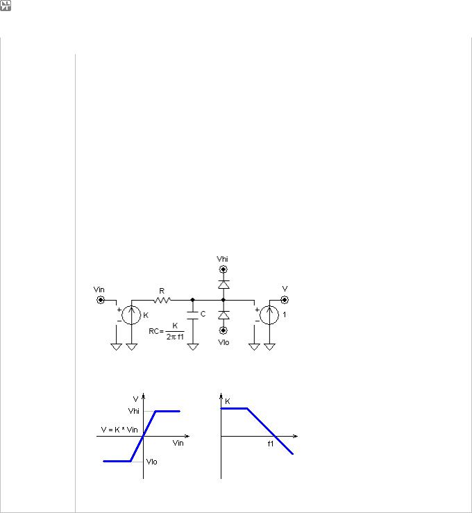
NL5 circuit simulator |
|
|
Руководство Пользователя |
|
|||
|
|
|
|
|
|
|
|
O |
|
Amplifier |
|
|
|
O/O_Amplifier_OpAmp.nl5 |
|
|
|
|
|
|
|
|
|
|
Model |
Parameter |
Units |
Description |
|
||
|
|
|
|
|
|
|
|
OpAmp |
K |
V/V |
Gain |
|
|||
|
|
|
|
|
|||
f1 |
Hz |
Unit gain frequency. |
|
||||
|
|
|
|
||||
|
|
|
|
|
|
|
|
|
|
|
Vhi |
V |
Max output voltage. |
|
|
|
|
|
|
|
|
|
|
|
|
|
Vlo |
V |
Min output voltage. |
|
|
|
|
|
|
|
|
|
|
|
|
|
IC |
V |
Initial condition: output voltage. |
|
|
|
|
|
|
|
|
|
|
Linear amplifier with output limiter. “K” is open loop gain. Frequency response consists of one pole, “f1” is unit gain frequency. “K” and “f1” can be set to infinity (“inf”). Output voltage is limiting between “Vlo” and “Vhi”.
When calculating DC operating point, if “f1” is not infinity and “IC” is defined, amplifier output is set to specified output voltage “IC”. If “IC” is blank, static characteristic is used.
Please note: if both “K” and “f1” are set to infinity, the model may experience convergence problem. Use Comparator model instead.
Equivalent schematic
Static characteristic |
AC response |
364
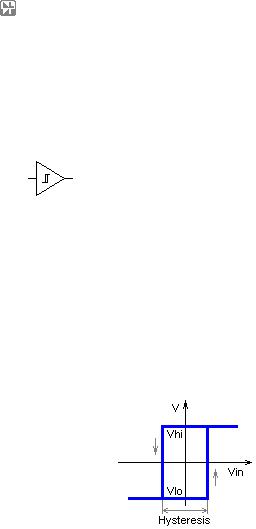
NL5 circuit simulator |
|
|
|
Руководство Пользователя |
|
||||
|
|
|
|
|
|
|
|
|
|
O |
|
Amplifier |
|
|
|
|
|
O/O_Amplifier_Comparator.nl5 |
|
|
|
|
|
|
|
|
|
|
|
|
Model |
Parameter |
|
Units |
Description |
|
|||
|
|
|
|
|
|
|
|
||
Comparator |
Hysteresis |
|
V |
Hysteresis |
|
||||
|
|
|
|
|
|
|
|||
Vhi |
|
V |
Max output voltage. |
|
|||||
|
|
|
|
|
|||||
|
|
|
|
|
|
|
|
||
|
|
|
Vlo |
|
V |
Min output voltage. |
|
||
|
|
|
|
|
|
|
|
||
|
|
|
Delay |
|
s |
Output delay. |
|
||
|
|
|
|
|
|
|
|
||
|
|
|
IC |
|
|
Initial condition: Low/High. |
|
||
|
|
|
|
|
|
|
|||
|
|
|
Comparator with hysteresis. Comparator output is set to “Vhi” or “Vlo” using following rules: |
|
|||||
|
|
|
Vin > Hysteresis/2 . . . : |
V = Vhi |
|
||||
|
|
|
Vin < - Hysteresis/2 . . : |
V = Vlo |
|
||||
|
|
|
Otherwise . . . . . . . . . .: |
V = previous state |
|
||||
|
|
|
The output is delayed by “Delay” time. Input pulses shorter than “Delay” will not pass through |
|
|||||
|
|
|
and will not affect output. |
|
|
|
|||
|
|
|
When calculating DC operating point comparator output is set to “Vlo” or to “Vhi”, according to |
|
|||||
|
|
|
selected “IC”. |
|
|
|
|
|
|
|
|
|
Static characteristic |
|
|
|
|||
|
|
|
|
|
|
|
|
|
|
365

NL5 circuit simulator |
|
|
Руководство Пользователя |
|
|||
|
|
|
|
|
|
|
|
O |
|
Amplifier |
|
|
|
O/O_Amplifier_Function.nl5 |
|
|
|
|
|
|
|
|
|
|
Model |
Parameter |
Units |
Description |
|
||
|
|
|
|
|
|
|
|
Function |
F(x) |
V |
Output as function of the input. |
|
|||
|
|
|
|
|
|||
F(s) |
|
AC transfer function in s domain. |
|
||||
|
|
|
|
|
|||
|
|
|
|
|
|
|
|
|
|
|
IC |
V |
Initial condition: output voltage. |
|
|
|
|
|
|
|
|
|
|
Arbitrary function.
Transient analysis. F(x) defines output voltage as a function of the following variables:
x – input voltage Vin t - current time
V(name) - voltage on the component name I(name) - current through the component name P(name) – power on the component name
where name is the name of any component in the schematic. If F(x) is blank, output is zero. F(s) is ignored.
Example:
F(x) = x*x
F(x) = x * sin(t)
F(x) = P(r1)+P(r2)
Please note that input voltage x, and variables V, I, and P are taken at previous calculation step. This may affect stability of the schematic with closed loop.
AC analysis. F(s) defines transfer function in s domain. Only operators and functions that support complex numbers can be used in this function. The following variables can be used in the function:
f – current AC frequency, Hz
w – angular AC frequency, w = 2πf .
s or p – Laplace parameter, s = p = j*2πf.
z – Z-transform parameter, is defined by custom formula in the Advanced Settings dialog box.
Example:
F(s) = 1/(1+s)
F(s) = exp(-1mk*s)
F(s) is calculated at each frequency. If F(s) is blank, it is assumed to be 1. Also, if F(x) is not blank, it is linearized at DC operating point, and F(s) is multiplied by linearized gain.
When calculating DC operating point for transient or AC analysis, output is set to specified output voltage “IC”.
366

NL5 circuit simulator |
|
|
Руководство Пользователя |
|
|||
|
|
|
|
|
|
|
|
O |
|
Amplifier |
|
|
|
O/O_Amplifier_PWL.nl5 |
|
|
|
|
|
|
|
|
|
|
Model |
Parameter |
Units |
Description |
|
||
|
|
|
|
|
|
|
|
|
PWL |
pwl |
|
Comma-separated string, K(Vin) |
|
||
|
|
|
|
|
|
||
|
Piece-wise linear amplifier. Amplifier gain K is defined by “pwl” string as a function of input |
|
|||||
|
|
|
|
||||
|
|
|
voltage Vin. See Working with PWL model chapter for details. |
|
|||
|
|
|
|
|
|
|
|
|
|
|
|
|
|
|
|
O |
|
Amplifier |
|
|
|
O/O_Amplifier_SubCir.nl5 |
|
|
|
|
|
|
|
|
|
|
Model |
Parameter |
Units |
Description |
|
||
|
|
|
|
|
|
|
|
SubCir |
File |
|
File name of subcircuit schematic. |
|
|||
|
|
|
|
|
|||
Pin1 |
|
Name of subcircuit label connected to pin 1 |
|
||||
|
|
|
|
|
|||
|
|
|
|
|
|
|
|
|
|
|
Pin2 |
|
Name of subcircuit label connected to pin 2 |
|
|
|
|
|
|
|
|
|
|
|
|
|
Cmd |
|
Subcircuit start-up command string |
|
|
|
|
|
|
|
|
|
|
|
|
|
IC |
|
Subcircuit Initial conditions string |
|
|
|
|
|
|
|
|
|
|
|
|
|
Subcircuit. See Working with Subcircuits chapter for details. |
|
|||
|
|
|
|
|
|
|
|
367

NL5 circuit simulator |
Руководство Пользователя |
O Differential
amplifier
Models
Linear
OpAmp
Comparator
Function
PWL
SubCir
Traces
I
Vin
V
P = V • I
O |
|
Differential amplifier |
|
|
O/O_DiffAmp_Linear.nl5 |
||
|
|
|
|
|
|
|
|
|
Model |
Parameter |
Units |
Description |
|||
|
|
|
|
|
|
||
Linear |
K |
V/V |
Gain |
||||
|
|
|
|
||||
f1 |
Hz |
Unit gain frequency. |
|||||
|
|
|
|||||
|
|
|
|
|
|
||
|
|
|
IC |
V |
Initial condition: output voltage. |
||
|
|
|
|
|
|
|
|
Linear differential amplifier. “K” is open loop gain. Frequency response consists of one pole, “f1” is unit gain frequency. “K” and “f1” can be set to infinity (“inf”).
When calculating DC operating point, if “f1” is not infinity and “IC” is defined, amplifier output is set to specified output voltage “IC”. If “IC” is blank, static characteristic is used.
Equivalent schematic
Static characteristic |
AC response |
368
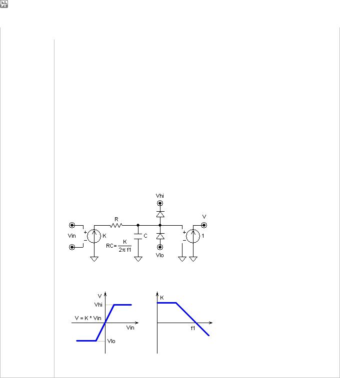
NL5 circuit simulator |
|
|
Руководство Пользователя |
|
|||
|
|
|
|
|
|
|
|
O |
|
Differential amplifier |
|
|
O/O_DiffAmp_OpAmp.nl5 |
|
|
|
|
|
|
|
|
|
|
|
Model |
Parameter |
Units |
Description |
|
||
|
|
|
|
|
|
|
|
OpAmp |
K |
V/V |
Gain |
|
|||
|
|
|
|
|
|||
f1 |
Hz |
Unit gain frequency. |
|
||||
|
|
|
|
||||
|
|
|
|
|
|
|
|
|
|
|
Vhi |
V |
Max output voltage. |
|
|
|
|
|
|
|
|
|
|
|
|
|
Vlo |
V |
Min output voltage. |
|
|
|
|
|
|
|
|
|
|
|
|
|
IC |
V |
Initial condition: output voltage. |
|
|
|
|
|
|
|
|
|
|
Linear amplifier with output limiter. “K” is open loop gain. Frequency response consists of one pole, “f1” is unit gain frequency. “K” and “f1” can be set to infinity (“inf”). Output voltage is limiting between “Vlo” and “Vhi”.
When calculating DC operating point, if “f1” is not infinity and “IC” is defined, amplifier output is set to specified output voltage “IC”. If “IC” is blank, static characteristic is used.
Please note: if both “K” and “f1” are set to infinity, the model may experience convergence problem. Use Comparator model instead.
Equivalent schematic
Static characteristic |
AC response |
369
NL5 circuit simulator |
|
|
Руководство Пользователя |
|
|||
|
|
|
|
|
|
|
|
O |
|
Differential amplifier |
|
|
O/O_DiffAmp_Comparator.nl5 |
|
|
|
|
|
|
|
|
|
|
|
Model |
Parameter |
Units |
Description |
|
||
|
|
|
|
|
|
|
|
Comparator |
Hysteresis |
V |
Hysteresis |
|
|||
|
|
|
|
|
|||
Vhi |
V |
Max output voltage. |
|
||||
|
|
|
|
||||
|
|
|
|
|
|
|
|
|
|
|
Vlo |
V |
Min output voltage. |
|
|
|
|
|
|
|
|
|
|
|
|
|
Delay |
s |
Output delay. |
|
|
|
|
|
|
|
|
|
|
|
|
|
IC |
|
Initial condition: Low/High. |
|
|
|
|
|
|
|
|
|
|
Comparator with hysteresis. Comparator output is set to “Vhi” or “Vlo” using following rules:
Vin > Hysteresis/2. . . . : V = Vhi
Vin < - Hysteresis/2. . . : V = Vlo
Otherwise . . . . . . . . . . : V = previous state
The output is delayed by “Delay” time. Input pulses shorter than “Delay” will not pass through and will not affect output.
When calculating DC operating point comparator output is set to “Vlo” or to “Vhi”, according to selected “IC”.
Static characteristic
370

NL5 circuit simulator |
|
|
Руководство Пользователя |
|
|||
|
|
|
|
|
|
|
|
O |
|
Differential amplifier |
|
|
O/O_DiffAmp_Function.nl5 |
|
|
|
|
|
|
|
|
|
|
|
Model |
Parameter |
Units |
Description |
|
||
|
|
|
|
|
|
|
|
Function |
F(x) |
V |
Output as function of the input. |
|
|||
|
|
|
|
|
|||
F(s) |
|
AC transfer function in s domain. |
|
||||
|
|
|
|
|
|||
|
|
|
|
|
|
|
|
|
|
|
IC |
V |
Initial condition: output voltage. |
|
|
|
|
|
|
|
|
|
|
Arbitrary function.
Transient analysis. F(x) defines output voltage as a function of the following variables:
x – input voltage Vin t - current time
V(name) - voltage on the component name I(name) - current through the component name P(name) – power on the component name
where name is the name of any component in the schematic. If F(x) is blank, output is zero. F(s) is ignored.
Example:
F(x) = x*x
F(x) = x * sin(t)
F(x) = P(r1)+P(r2)
Please note that input voltage x, and variables V, I, and P are taken at previous calculation step. This may affect stability of the schematic with closed loop.
AC analysis. F(s) defines transfer function in s domain. Only operators and functions that support complex numbers can be used in this function. The following variables can be used in the function:
f – current AC frequency, Hz
w – angular AC frequency, w = 2πf .
s or p – Laplace parameter, s = p = j*2πf.
z – Z-transform parameter, is defined by custom formula in the Advanced Settings dialog box.
Example:
F(s) = 1/(1+s)
F(s) = exp(-1mk*s)
F(s) is calculated at each frequency. If F(s) is blank, it is assumed to be 1. Also, if F(x) is not blank, it is linearized at DC operating point, and F(s) is multiplied by linearized gain.
When calculating DC operating point for transient or AC analysis, output is set to specified output voltage “IC”.
371

NL5 circuit simulator |
|
|
Руководство Пользователя |
|
|||
|
|
|
|
|
|
|
|
O |
|
Differential amplifier |
|
|
O/O_DiffAmp_PWL.nl5 |
|
|
|
|
|
|
|
|
|
|
|
Model |
Parameter |
Units |
Description |
|
||
|
|
|
|
|
|
|
|
|
PWL |
pwl |
|
Comma-separated string, K(Vin) |
|
||
|
|
|
|
|
|
||
|
Piece-wise linear amplifier. Amplifier gain K is defined by “pwl” string as a function of input |
|
|||||
|
|
|
|
||||
|
|
|
voltage Vin. See Working with PWL model chapter for details. |
|
|||
|
|
|
|
|
|
|
|
|
|
|
|
|
|
|
|
O |
|
Differential amplifier |
|
|
O/O_DiffAmp_SubCir.nl5 |
|
|
|
|
|
|
|
|
|
|
|
Model |
Parameter |
Units |
Description |
|
||
|
|
|
|
|
|
|
|
SubCir |
File |
|
File name of subcircuit schematic. |
|
|||
|
|
|
|
|
|||
Pin1 |
|
Name of subcircuit label connected to pin 1 |
|
||||
|
|
|
|
|
|||
|
|
|
|
|
|
|
|
|
|
|
Pin2 |
|
Name of subcircuit label connected to pin 2 |
|
|
|
|
|
|
|
|
|
|
|
|
|
Pin3 |
|
Name of subcircuit label connected to pin 3 |
|
|
|
|
|
|
|
|
|
|
|
|
|
Cmd |
|
Subcircuit start-up command string |
|
|
|
|
|
|
|
|
|
|
|
|
|
IC |
|
Subcircuit Initial conditions string |
|
|
|
|
|
|
|
|
|
|
Subcircuit. See Working with Subcircuits chapter for details.
372
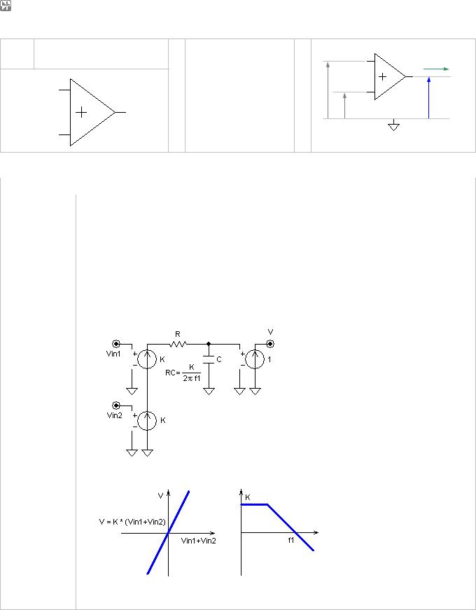
NL5 circuit simulator |
Руководство Пользователя |
O
Summing
amplifier
Models
Linear
OpAmp
Function
PWL
SubCir
Traces
I
Vin1
V
Vin2
P = V • I
O |
Summing amplifier |
|
|
O/O_SumAmp_Linear.nl5 |
||
|
|
|
|
|
|
|
Model |
Parameter |
Units |
Description |
|||
|
|
|
|
|
||
Linear |
K |
V/V |
Gain |
|||
|
|
|
|
|||
f1 |
Hz |
Unit gain frequency. |
||||
|
|
|||||
|
|
|
|
|
||
|
|
IC |
V |
Initial condition: output voltage. |
||
|
|
|
|
|
|
|
Linear summing amplifier. “K” is open loop gain. Frequency response consists of one pole, “f1” is unit gain frequency. “K” and “f1” can be set to infinity (“inf”).
When calculating DC operating point, if “f1” is not infinity and “IC” is defined, amplifier output is set to specified output voltage “IC”. If “IC” is blank, static characteristic is used.
Equivalent schematic
Static characteristic |
AC response |
373
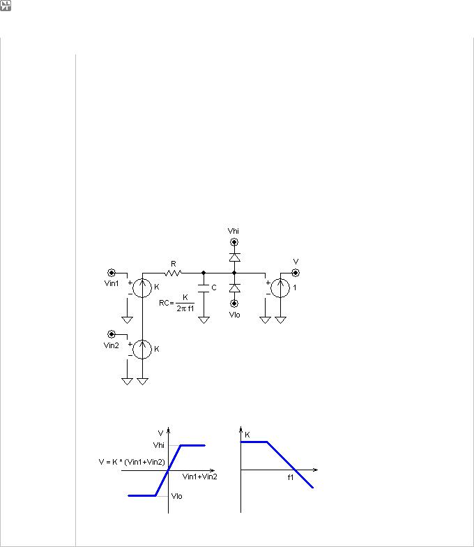
NL5 circuit simulator |
|
|
Руководство Пользователя |
|
|||
|
|
|
|
|
|
|
|
O |
|
Summing amplifier |
|
|
O/O_SumAmp_OpAmp.nl5 |
|
|
|
|
|
|
|
|
|
|
|
Model |
Parameter |
Units |
Description |
|
||
|
|
|
|
|
|
|
|
OpAmp |
K |
V/V |
Gain |
|
|||
|
|
|
|
|
|||
f1 |
Hz |
Unit gain frequency. |
|
||||
|
|
|
|
||||
|
|
|
|
|
|
|
|
|
|
|
Vhi |
V |
Max output voltage. |
|
|
|
|
|
|
|
|
|
|
|
|
|
Vlo |
V |
Min output voltage. |
|
|
|
|
|
|
|
|
|
|
|
|
|
IC |
V |
Initial condition: output voltage. |
|
|
|
|
|
|
|
|
|
|
Linear amplifier with output limiter. “K” is open loop gain. Frequency response consists of one pole, “f1” is unit gain frequency. “K” and “f1” can be set to infinity (“inf”). Output voltage is limiting between “Vlo” and “Vhi”.
When calculating DC operating point, if “f1” is not infinity and “IC” is defined, amplifier output is set to specified output voltage “IC”. If “IC” is blank, static characteristic is used.
Equivalent schematic
Static characteristic |
AC response |
374

NL5 circuit simulator |
|
|
Руководство Пользователя |
|
|||
|
|
|
|
|
|
||
O |
|
Summing amplifier |
|
|
O/O_SumAmp_Function.nl5 |
||
|
|
|
|
|
|
|
|
|
Model |
Parameter |
Units |
Description |
|||
|
|
|
|
|
|
||
Function |
F(x) |
V |
Output as function of the input. |
||||
|
|
|
|
|
|||
F(s) |
|
AC transfer function in s domain. |
|||||
|
|
|
|
||||
|
|
|
|
|
|
||
|
|
|
IC |
V |
Initial condition: output voltage. |
||
|
|
|
|
|
|
|
|
Arbitrary function.
Transient analysis. F(x) defines output voltage as a function of the following variables:
x – voltage Vin1+Vin2 t - current time
V(name) - voltage on the component name I(name) - current through the component name P(name) – power on the component name
where name is the name of any component in the schematic. If F(x) is blank, output is zero. F(s) is ignored.
Example:
F(x) = x*x
F(x) = x * sin(t)
F(x) = P(r1)+P(r2)
Please note that input voltage x, and variables V, I, and P are taken at previous calculation step. This may affect stability of the schematic with closed loop.
AC analysis. F(s) defines transfer function in s domain. Only operators and functions that support complex numbers can be used in this function. The following variables can be used in the function:
f – current AC frequency, Hz
w – angular AC frequency, w = 2πf .
s or p – Laplace parameter, s = p = j*2πf.
z – Z-transform parameter, is defined by custom formula in the Advanced Settings dialog box.
Example:
F(s) = 1/(1+s)
F(s) = exp(-1mk*s)
F(s) is calculated at each frequency. If F(s) is blank, it is assumed to be 1. Also, if F(x) is not blank, it is linearized at DC operating point, and F(s) is multiplied by linearized gain.
When calculating DC operating point for transient or AC analysis, output is set to specified output voltage “IC”.
375

NL5 circuit simulator |
|
|
Руководство Пользователя |
|
|||
|
|
|
|
|
|
|
|
O |
|
Summing amplifier |
|
|
O/O_SumAmp_PWL.nl5 |
||
|
|
|
|
|
|
|
|
|
Model |
Parameter |
Units |
Description |
|||
|
|
|
|
|
|||
|
PWL |
pwl |
|
Comma-separated string, K(Vin1+Vin2) |
|||
|
|
|
Piece-wise linear amplifier. Amplifier gain K is defined by “pwl” string as a function of sum of |
||||
|
|
|
input voltages Vin1+Vin2. See Working with PWL model chapter for details. |
||||
|
|
|
|
|
|
|
|
|
|
|
|
|
|
||
O |
|
Summing amplifier |
|
|
O/O_SumAmp_SubCir.nl5 |
||
|
|
|
|
|
|
|
|
|
Model |
Parameter |
Units |
Description |
|||
|
|
|
|
|
|
||
SubCir |
File |
|
File name of subcircuit schematic. |
||||
|
|
|
|
|
|||
Pin1 |
|
Name of subcircuit label connected to pin 1 |
|||||
|
|
|
|
||||
|
|
|
|
|
|
||
|
|
|
Pin2 |
|
Name of subcircuit label connected to pin 2 |
||
|
|
|
|
|
|
||
|
|
|
Pin3 |
|
Name of subcircuit label connected to pin 3 |
||
|
|
|
|
|
|
||
|
|
|
Cmd |
|
Subcircuit start-up command string |
||
|
|
|
|
|
|
||
|
|
|
IC |
|
Subcircuit Initial conditions string |
||
|
|
|
|
|
|
||
|
|
|
Subcircuit. See Working with Subcircuits chapter for details. |
||||
|
|
|
|
|
|
|
|
376
NL5 circuit simulator |
Руководство Пользователя |
O |
Voltage controlled |
|
PWL |
|
amplifier |
|
|
||
|
|
Models |
|
Traces |
|
|
|
||
|
|
|
|
|
Views
I
Vin |
V |
|
|
|
Vc |
P = V • I
O |
Voltage controlled amplifier |
|
O/O_VCA_PWL.nl5 |
||
|
|
|
|
|
|
Model |
Parameter |
Units |
Description |
||
|
|
|
|
|
|
PWL |
pwl |
|
Comma-separated string, K(Vc) |
||
|
|
|
|
||
|
|
|
|
||
Piece-wise linear voltage controlled amplifier. At any moment, the amplifier is a linear amplifier. Its gain K is a function of control voltage:
V = K(Vc)*Vin.
“pwl” string defines gain K as a function of control voltage Vc. See Working with PWL model chapter for details.
377
NL5 circuit simulator |
Руководство Пользователя |
O |
Current controlled |
|
PWL |
|
amplifier |
|
|
||
|
|
Models |
|
Traces |
|
|
|
||
|
|
|
|
|
Views
I
Vin |
V |
|
|
|
Ic |
P = V • I
O |
Current controlled amplifier |
|
O/O_CCA_PWL.nl5 |
||
|
|
|
|
|
|
Model |
Parameter |
Units |
Description |
||
|
|
|
|
|
|
PWL |
pwl |
|
Comma-separated string, K(Ic) |
||
|
|
|
|
||
|
|
|
|
||
Piece-wise linear current controlled amplifier. At any moment, the amplifier is a linear amplifier. Its gain K is a function of control current:
V = K(Ic)*Vin.
“pwl” string defines gain K as a function of control current Ic. See Working with PWL model chapter for more details.
378

NL5 circuit simulator |
Руководство Пользователя |
R
Resistor
Models
R PWL PWL-I
Function SubCir
Traces
V  I
I
P = V • I
R |
|
Resistor |
|
|
|
R/R_Resistor_R.nl5 |
|
|
|
|
|
|
|
|
Model |
Parameter |
Units |
Description |
||
|
|
|
|
|
|
|
|
R |
R |
Ohm |
Resistance |
||
|
|
|
|
|
||
|
Linear resistor. V = R*I. |
|||||
|
|
|
||||
|
|
|
|
|
|
|
|
|
|
|
|
|
|
R |
|
Resistor |
|
|
|
R/R_Resistor_PWL.nl5 |
|
|
|
|
|
|
|
|
Model |
Parameter |
Units |
Description |
||
|
|
|
|
|
|
|
|
PWL |
pwl |
|
Comma-separated string, R(V) |
||
|
|
|
|
|
||
|
|
|
|
|
||
Piece-wise linear resistor. “pwl” string defines resistance as a function of voltage across the resitor R(V). See Working with PWL model chapter for details.
R |
Resistor |
|
|
|
R/R_Resistor_PWL-I.nl5 |
|
|
|
|
|
|
Model |
Parameter |
Units |
Description |
||
|
|
|
|
|
|
PWL-I |
pwl |
|
Comma-separated string, R(I) |
||
|
|
|
|
||
|
|
|
|
||
Piece-wise linear resistor. “pwl” string defines resistance as a function of current through the resistor R(I). See Working with PWL model chapter for details.
379
NL5 circuit simulator |
|
|
Руководство Пользователя |
|
|||
|
|
|
|
|
|
|
|
R |
|
Resistor |
|
|
|
R/R_Resistor_Function.nl5 |
|
|
|
|
|
|
|
|
|
|
Model |
Parameter |
Units |
Description |
|
||
|
|
|
|
|
|
|
|
Function |
Z(s) |
Ohm |
Impedance as a function of s parameter. |
|
|||
|
|
|
|
|
|||
Impedance function in s domain. For transient, constant impedance Z(0) is used. For |
|
||||||
|
|
|
|
||||
|
|
|
linearized AC analysis, complex impedance Z(s) is used. The following variables can be used |
|
|||
|
|
|
in the function: |
|
|
|
|
|
|
|
f – current AC frequency, Hz |
|
|||
|
|
|
w – angular AC frequency, w = 2πf . |
|
|||
|
|
|
s or p – Laplace parameter, s = p = j*2πf. |
|
|||
|
|
|
z – Z-transform parameter, is defined by custom formula in the Advanced Settings |
|
|||
|
|
|
dialog box. |
|
|
|
|
|
|
|
Example: |
|
|
|
|
|
|
|
Z(s) = 10+3n*s |
- 10 Ohm resistor in series with 3 nH inductor. |
|
||
|
|
|
Z(s) = 10||(1.0/3p/s) - 10 Ohm resistor in parallel with 3 pF capacitor. |
|
|||
|
|
|
|
|
|
|
|
|
|
|
|
|
|
|
|
R |
|
Resistor |
|
|
|
R/R_Resistor_SubCir.nl5 |
|
|
|
|
|
|
|
|
|
|
Model |
Parameter |
Units |
Description |
|
||
|
|
|
|
|
|
|
|
SubCir |
File |
|
File name of subcircuit schematic. |
|
|||
|
|
|
|
|
|||
Pin1 |
|
Name of subcircuit label connected to pin 1 |
|
||||
|
|
|
|
|
|||
|
|
|
|
|
|
|
|
|
|
|
Pin2 |
|
Name of subcircuit label connected to pin 2 |
|
|
|
|
|
|
|
|
|
|
|
|
|
Cmd |
|
Subcircuit start-up command string |
|
|
|
|
|
|
|
|
|
|
|
|
|
IC |
|
Subcircuit Initial conditions string |
|
|
|
|
|
|
|
|
|
|
|
|
|
Subcircuit. See Working with Subcircuits chapter for details. |
|
|||
|
|
|
|
|
|
|
|
380
NL5 circuit simulator |
Руководство Пользователя |
R |
Potentiometer |
|
Potentiometer |
|
|
|
Models |
|
Traces |
|
|
|
|
|
R*(1-Position)
V
R*Position
R |
Potentiometer |
|
|
|
R/R_Potentiometer_Potentiometer.nl5 |
|
|
|
|
|
|
|
Model |
Parameter |
Units |
Description |
|
|
|
|
|
|
|
Potentiometer |
R |
Ohm |
Resistance |
||
|
|
|
|
||
Position |
|
Position of the wiper (0…1) |
|||
|
|
|
|||
|
|
|
|
|
|
Potentiometer. Position of the wiper is referenced to the terminal with dot:
0 – wiper is connected to the terminal with dot 1 – wiper is connected to another terminal.
381
NL5 circuit simulator |
Руководство Пользователя |
R |
Voltage controlled |
|
PWL |
|
resistor |
|
|
||
|
|
|
||
|
|
Models |
|
Traces |
|
|
|
|
|
Views
V in |
V I |
|||
|
|
|
|
|
P = V • I |
|
|
||
R |
Voltage controlled resistor |
|
R/R_VCR_PWL.nl5 |
||
|
|
|
|
|
|
Model |
Parameter |
Units |
Description |
||
|
|
|
|
|
|
PWL |
pwl |
|
Comma-separated string, R(Vin) |
||
|
|
|
|
||
|
|
|
|
||
Piece-wise linear voltage controlled resistor. At any moment, resistor is a linear resistor. Its resistance R is a function of control voltage:
V = R(Vin)*I.
“pwl” string defines resistance as a function of control voltage Vin. See Working with PWL model chapter for details.
382
NL5 circuit simulator |
Руководство Пользователя |
R |
Current controlled |
|
PWL |
|
resistor |
|
|
||
|
|
|
||
|
|
Models |
|
Traces |
|
|
|
|
|
Views
I in |
V I |
|
P = V • I |
|
|
|
|
|
R |
Current controlled resistor |
|
R/R_CCR_PWL.nl5 |
||
|
|
|
|
|
|
Model |
Parameter |
Units |
Description |
||
|
|
|
|
|
|
PWL |
pwl |
|
Comma-separated string, R(Iin) |
||
|
|
|
|
||
|
|
|
|
||
Piece-wise linear current controlled resistor. At any moment, resistor is a linear resistor. Its resistance R is a function of control current:
V = R(Iin)*I.
“pwl” string defines resistance as a function of control current Iin. See Working with PWL model chapter for details.
383
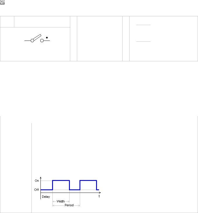
NL5 circuit simulator |
Руководство Пользователя |
S
Switch
Models
Switch
Pulse
Step
List
File
SubCir
Traces
V

 I
I
P = V • I
S |
|
Switch |
|
|
|
S/S_Switch_Switch.nl5 |
|
|
|
|
|
|
|
|
|
|
Model |
Parameter |
Units |
Description |
|||
|
|
|
|
|
|
||
Switch |
Switch |
|
Switch state: Off/On. |
||||
|
|
|
|
||||
Switch. Off – open switch, infinite resistance. On – closed switch, zero resistance. |
|||||||
|
|
|
|||||
|
|
|
|
|
|
|
|
|
|
|
|
|
|
|
|
S |
|
Switch |
|
|
|
S/S_Switch_Pulse.nl5 |
|
|
|
|
|
|
|
|
|
|
Model |
Parameter |
Units |
Description |
|||
|
|
|
|
|
|
||
|
Pulse |
Period |
s |
Period. |
|||
|
|
|
|
|
|||
|
Width |
s |
Pulse width. |
||||
|
|
|
|||||
|
|
|
|
|
|
||
|
|
|
Delay |
s |
Delay before first pulse starts. |
||
|
|
|
|
|
|
||
|
|
|
Active |
|
Active switch state: Off/On. |
||
|
|
|
|
|
|
|
|
Pulse switch. Switching starts after “Delay” time. Switch is in active state during “Width” time.
The following switching diagram is shown for “Active” = On:
384
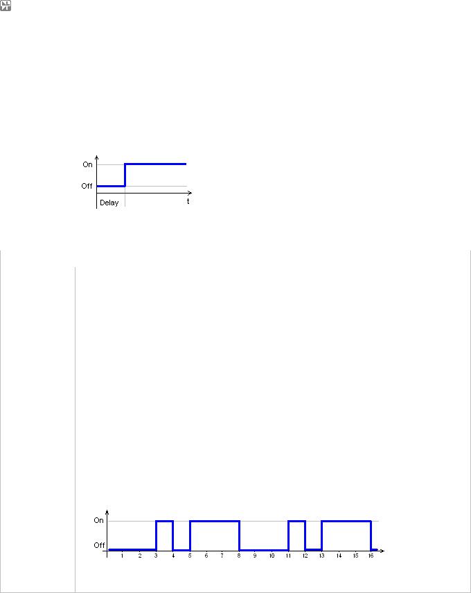
NL5 circuit simulator |
|
|
Руководство Пользователя |
|
|||
|
|
|
|
|
|
|
|
S |
|
Switch |
|
|
|
S/S_Switch_Step.nl5 |
|
|
|
|
|
|
|
|
|
|
Model |
Parameter |
Units |
Description |
|
||
|
|
|
|
|
|
|
|
|
Step |
Delay |
s |
Delay before active state. |
|
||
|
|
|
|
|
|
||
|
Active |
|
Active switch state: Off/On. |
|
|||
|
|
|
|
|
|||
|
|
|
|
|
|
|
|
|
|
|
Step switch. Switch is in active state after “Delay” time. |
|
|||
|
|
|
The following switching diagram is shown for “Active” = On: |
|
|||
|
|
|
|
|
|
|
|
|
|
|
|
|
|
|
|
S |
|
Switch |
|
|
|
V/S_Switch_List.nl5 |
|
|
|
|
|
|
|
|
|
|
Model |
Parameter |
Units |
Description |
|
||
|
|
|
|
|
|
|
|
|
List |
List |
|
Comma-separated string. |
|
||
|
|
|
|
|
|
||
|
Cycle |
|
Cycling (repeat): No/Yes. |
|
|||
|
|
|
|
|
|||
|
|
|
|
|
|
|
|
|
|
|
Delay |
s |
Delay. |
|
|
|
|
|
|
|
|
|
|
List switch. Switching sequence is defined in the “List” parameter in the csv (“commaseparated values”) format, as follows:
t0,s0,t1,s1,...,tn,sn
s0…sn defines switch state: positive number corresponds to On state, zero or negative number - Off state. If t<t0, switch is in s0 state. At t0 switch is set to s0 state. At t1 switch is set to s1 state, and so on. At t>tn, switch remains in sn state if “Cycle” parameter is set to “No”, otherwise states sequence defined in t0…tn interval is repeated continuously. In addition, the whole signal is delayed by “Delay” time.
Example:
List = 0,0,3,1,4,0,5,1,8,0
The following switching diagram is shown for “Cycle” = Yes, “Delay” = 0:
See Working with List model chapter for more details.
385
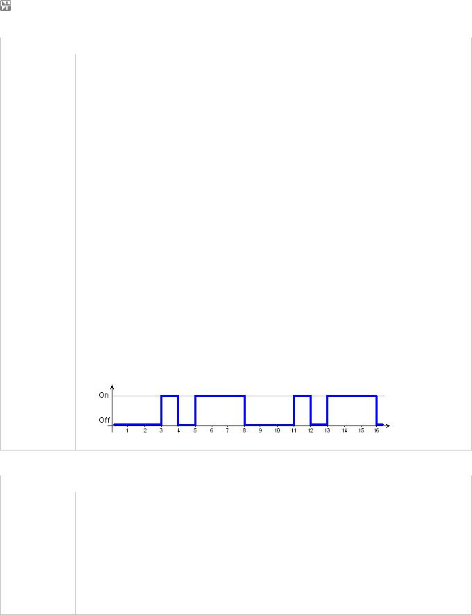
NL5 circuit simulator |
|
|
Руководство Пользователя |
|
|||
|
|
|
|
|
|
|
|
S |
|
Switch |
|
|
|
V/S_Switch_File.nl5 |
|
|
|
|
|
|
|
|
|
|
Model |
Parameter |
Units |
Description |
|
||
|
|
|
|
|
|
|
|
|
File |
File |
|
File name. |
|
||
|
|
|
|
|
|
||
|
Cycle |
|
Cycling (repeat): No/Yes. |
|
|||
|
|
|
|
|
|||
|
|
|
|
|
|
|
|
|
|
|
Delay |
s |
Delay. |
|
|
|
|
|
|
|
|
|
|
File switch. Switching sequence is defined in the text file. “File“ parameter is a file name, with full path to the file. If the file is located in the same directory as schematic file, the path can be omitted. Switching sequence is defined in the csv (“comma-separated values”) format, as follows:
<if first line does not start with a number, it is ignored> t0,s0
t1,s1
.....
tn,sn
s0…sn defines switch state: positive number corresponds to On state, zero or negative number - Off state. If t<t0, switch is in s0 state. At t0 switch is set to s0 state. At t1 switch is set to s1 state, and so on. At t>tn, switch remains in sn state if “Cycle” parameter is set to “No”, otherwise states sequence defined in t0…tn interval is repeated continuously. In addition, the whole signal is delayed by “Delay” time.
Example:
0,0
3,1
4,0
5,1
8,0
The following switching diagram is shown for “Cycle” = Yes, “Delay” = 0:
S |
|
Switch |
|
|
|
S/S_Switch_SubCir.nl5 |
|
|
|
|
|
|
|
|
Model |
Parameter |
Units |
Description |
||
|
|
|
|
|
|
|
SubCir |
File |
|
File name of subcircuit schematic. |
|||
|
|
|
|
|||
Pin1 |
|
Name of subcircuit label connected to pin 1 |
||||
|
|
|
|
|||
|
|
|
|
|
|
|
|
|
|
Pin2 |
|
Name of subcircuit label connected to pin 2 |
|
|
|
|
|
|
|
|
|
|
|
Cmd |
|
Subcircuit start-up command string |
|
|
|
|
|
|
|
|
|
|
|
IC |
|
Subcircuit Initial conditions string |
|
|
|
|
|
|
|
|
Subcircuit. See Working with Subcircuits chapter for details.
386

NL5 circuit simulator |
Руководство Пользователя |
S |
Logic controlled |
switch |
Models
Switch
Pulse
Steps
SubCir
Traces
V  I
I
V in
P = V • I
S |
|
Logic controlled switch |
|
|
|
|
S/S_LCS_Switch.nl5 |
|
|
|
|
|
|
|
|
|
|
|
Model |
Parameter |
Units |
|
Description |
|||
|
|
|
|
|
|
|
||
Switch |
Active |
|
|
Active state: Off/On. |
||||
|
|
|
|
|
|
|||
IC |
|
|
Initial condition: Off/On. |
|||||
|
|
|
|
|
||||
|
|
|
|
|
|
|||
|
|
|
Logic controlled switch. Switch is set to active or non-active state using following rules: |
|||||
|
|
|
Vin > logical threshold . . . : |
active |
||||
|
|
|
Vin < logical threshold . . . : |
non-active |
||||
|
|
|
To see and set logical levels and threshold go to Transient | Settings, or AC | Settings, then |
|||||
|
|
|
click Advanced button. |
|
|
|
||
|
|
|
When calculating DC operating point switch is set to the state defined in “IC”. |
|||||
|
|
|
|
|
|
|
|
|
|
|
|
|
|
|
|
|
|
S |
|
Logic controlled switch |
|
|
|
|
S/S_LCS_Pulse.nl5 |
|
|
|
|
|
|
|
|
||
|
Model |
Parameter |
Units |
|
Description |
|||
|
|
|
|
|
|
|
||
|
Pulse |
Width |
s |
|
Pulse width. |
|||
|
|
|
|
|
|
|
||
|
Active |
|
|
Active state: Off/On. |
||||
|
|
|
|
|
||||
|
|
|
One-shot pulse generator. When increasing input voltage Vin crosses logical threshold, |
|||||
|
|
|
switch is set to active state for “Width” time interval. If increasing Vin crosses logical threshold |
|||||
|
|
|
value while switch is in active state, the pulse is restarted. |
|||||
|
|
|
To see and set logical levels and threshold go to Transient | Settings, or AC | Settings, then |
|||||
|
|
|
click Advanced button. |
|
|
|
||
|
|
|
|
|
|
|
|
|
387
NL5 circuit simulator |
|
|
Руководство Пользователя |
|
|||
|
|
|
|
|
|
|
|
S |
|
Logic controlled switch |
|
|
S/S_LCS_Steps.nl5 |
|
|
|
|
|
|
|
|
|
|
|
Model |
Parameter |
Units |
Description |
|
||
|
|
|
|
|
|
|
|
|
Steps |
Roff |
Ohm |
Off state resistance. |
|
||
|
|
|
|
|
|
||
|
Ron |
Ohm |
On state resistance. |
|
|||
|
|
|
|
||||
|
|
|
|
|
|
|
|
|
|
|
Slope |
|
Type of resistance change: Linear/Cos/Log. |
|
|
|
|
|
|
|
|
|
|
|
|
|
Ramp |
s |
Resistance ramp time. |
|
|
|
|
|
|
|
|
|
|
|
|
|
Steps |
|
Number of resistance steps in the ramp. |
|
|
|
|
|
|
|
|
|
|
|
|
|
IC |
|
Initial condition: Off/On. |
|
|
|
|
|
|
|
|
|
|
Switch with resistance ramping. When increasing input voltage Vin crosses logical threshold, switch resistance starts ramping from “Roff” to “Ron”. When decreasing input voltage Vin crosses logical threshold, switch resistance starts ramping from “Ron” to “Roff”.
Resistance is changing during “Ramp” time interval, with number of steps specified by “Steps” parameter. If “Steps” = 0, resistance is changed instantly.
“Slope” parameter specifies how resistance is changing during he ramp. The following slope types are available (“Steps” = 6):
Linear Cos Log
To see and set logical levels and threshold go to Transient | Settings, or AC | Settings, then click Advanced button.
When calculating DC operating point switch is set to the state specified in “IC”.
S |
|
Logic controlled switch |
|
|
S/S_LCS_SubCir.nl5 |
|
|
|
|
|
|
|
|
|
Model |
Parameter |
Units |
Description |
||
|
|
|
|
|
|
|
SubCir |
File |
|
File name of subcircuit schematic. |
|||
|
|
|
|
|||
Pin1 |
|
Name of subcircuit label connected to pin 1 |
||||
|
|
|
|
|||
|
|
|
|
|
|
|
|
|
|
Pin2 |
|
Name of subcircuit label connected to pin 2 |
|
|
|
|
|
|
|
|
|
|
|
Pin3 |
|
Name of subcircuit label connected to pin 3 |
|
|
|
|
|
|
|
|
|
|
|
Pin4 |
|
Name of subcircuit label connected to pin 4 |
|
|
|
|
|
|
|
|
|
|
|
Cmd |
|
Subcircuit start-up command string |
|
|
|
|
|
|
|
|
|
|
|
IC |
|
Subcircuit Initial conditions string |
|
|
|
|
|
|
|
|
Subcircuit. See Working with Subcircuits chapter for details.
388
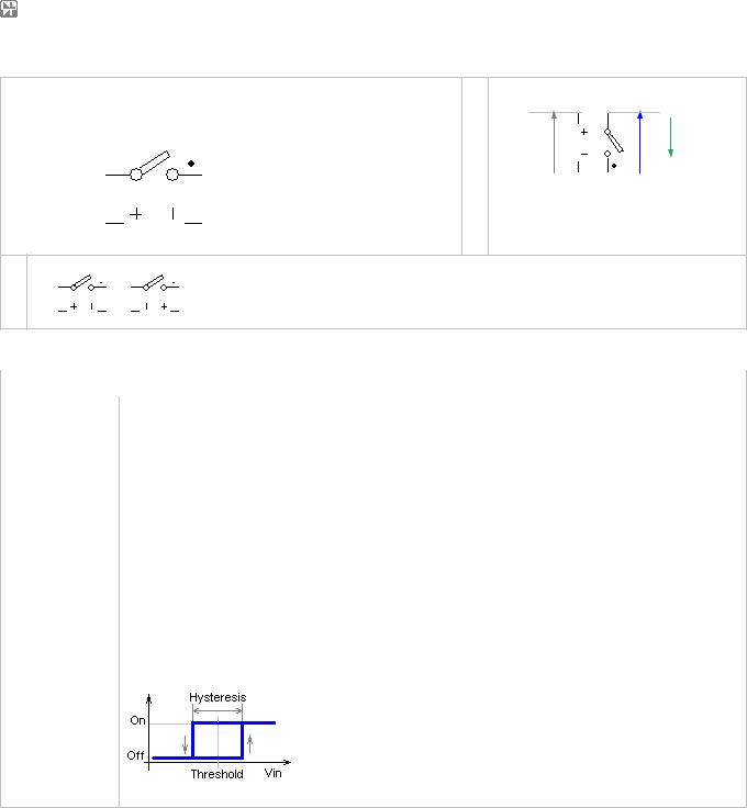
NL5 circuit simulator |
Руководство Пользователя |
S |
Voltage controlled |
|
Switch |
switch |
|
||
|
Pulse |
||
|
|
Models |
|
|
|
Steps |
|
|
|
SubCir |
|
|
|
|
|
|
|
|
|
Views
Traces
V in |
V I |
|||
|
|
|
|
|
P = V • I |
|
|
||
S |
|
Voltage controlled switch |
|
S/S_VCS_Switch.nl5 |
|||
|
|
|
|
|
|
|
|
|
Model |
Parameter |
Units |
Description |
|||
|
|
|
|
|
|
||
Switch |
Threshold |
V |
Voltage threshold. |
||||
|
|
|
|
||||
Hysteresis |
V |
Hysteresis. |
|||||
|
|
|
|||||
|
|
|
|
|
|
||
|
|
|
Active |
|
Active state: Off/On. |
||
|
|
|
|
|
|
||
|
|
|
IC |
|
Initial condition: Off/On. |
||
|
|
|
|
|
|
|
|
Voltage controlled switch. Switch is set to active or non-active state using following rules:
Vin > Threshold + Hysteresis/2. . . |
: |
active |
Vin < Threshold - Hysteresis/2 . . . |
: |
non-active |
Otherwise . . . . . . . . . . . . . . . . . . . |
: |
previous state |
When calculating DC operating point switch is set to the state defined in “IC”.
The following is switching diagram for “Active” = On:
389
NL5 circuit simulator |
|
|
Руководство Пользователя |
|
|||
|
|
|
|
|
|
|
|
S |
|
Voltage controlled switch |
|
S/S_VCS_Pulse.nl5 |
|
||
|
|
|
|
|
|
|
|
|
Model |
Parameter |
Units |
Description |
|
||
|
|
|
|
|
|
|
|
|
Pulse |
Width |
s |
Pulse width. |
|
||
|
|
|
|
|
|
||
|
Threshold |
V |
Voltage threshold. |
|
|||
|
|
|
|
||||
|
|
|
|
|
|
|
|
|
|
|
Active |
|
Active state: Off/On. |
|
|
|
|
|
|
|
|
|
|
|
|
|
One-shot pulse generator. When increasing input voltage Vin crosses “Threshold” value, |
|
|||
|
|
|
switch is set to active state for “Width” time interval. If increasing Vin crosses “Threshold” |
|
|||
|
|
|
value while switch is in active state, the pulse is restarted. |
|
|||
|
|
|
|
|
|
|
|
|
|
|
|
|
|
||
S |
|
Voltage controlled switch |
|
S/S_VCS_Steps.nl5 |
|
||
|
|
|
|
|
|
|
|
|
Model |
Parameter |
Units |
Description |
|
||
|
|
|
|
|
|
|
|
|
Steps |
Threshold |
V |
Voltage threshold. |
|
||
|
|
|
|
|
|
||
|
Hysteresis |
V |
Hysteresis. |
|
|||
|
|
|
|
||||
|
|
|
|
|
|
|
|
|
|
|
Roff |
Ohm |
Off state resistance. |
|
|
|
|
|
|
|
|
|
|
|
|
|
Ron |
Ohm |
On state resistance. |
|
|
|
|
|
|
|
|
|
|
|
|
|
Slope |
|
Type of resistance change: Linear/Cos/Log. |
|
|
|
|
|
|
|
|
|
|
|
|
|
Ramp |
s |
Resistance ramp time. |
|
|
|
|
|
|
|
|
|
|
|
|
|
Steps |
|
Number of resistance steps in the ramp. |
|
|
|
|
|
|
|
|
|
|
|
|
|
IC |
|
Initial condition: Off/On. |
|
|
|
|
|
|
|
|
|
|
Switch with resistance ramping. When increasing input voltage Vin crosses “Threshold” plus “Hysteresis”/2 value, switch resistance starts ramping from “Roff” to “Ron”. When decreasing input voltage Vin crosses “Threshold” minus “Hysteresis”/2 value, switch resistance starts ramping from “Ron” to “Roff”.
Resistance is changing during “Ramp” time interval, with number of steps specified by “Steps” parameter. If “Steps” = 0, resistance is changed instantly.
“Slope” parameter specifies how resistance is changing during he ramp. The following slope types are available (“Steps” = 6):
Linear |
Cos |
Log |
When calculating DC operating point switch is set to the state specified in “IC”.
390

NL5 circuit simulator |
|
|
Руководство Пользователя |
|
|||
|
|
|
|
|
|
|
|
S |
|
Voltage controlled switch |
|
S/S_VCS_SubCir.nl5 |
|
||
|
|
|
|
|
|
|
|
|
Model |
Parameter |
Units |
Description |
|
||
|
|
|
|
|
|
|
|
SubCir |
File |
|
File name of subcircuit schematic. |
|
|||
|
|
|
|
|
|||
Pin1 |
|
Name of subcircuit label connected to pin 1 |
|
||||
|
|
|
|
|
|||
|
|
|
|
|
|
|
|
|
|
|
Pin2 |
|
Name of subcircuit label connected to pin 2 |
|
|
|
|
|
|
|
|
|
|
|
|
|
Pin3 |
|
Name of subcircuit label connected to pin 3 |
|
|
|
|
|
|
|
|
|
|
|
|
|
Pin4 |
|
Name of subcircuit label connected to pin 4 |
|
|
|
|
|
|
|
|
|
|
|
|
|
Cmd |
|
Subcircuit start-up command string |
|
|
|
|
|
|
|
|
|
|
|
|
|
IC |
|
Subcircuit Initial conditions string |
|
|
|
|
|
|
|
|
|
|
|
|
|
Subcircuit. See Working with Subcircuits chapter for details. |
|
|||
|
|
|
|
|
|
|
|
391
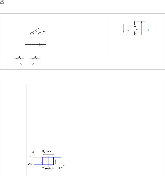
NL5 circuit simulator |
Руководство Пользователя |
S |
Current controlled |
|
Switch |
switch |
|
||
|
Pulse |
||
|
|
Models |
|
|
|
Steps |
|
|
|
SubCir |
|
|
|
|
|
|
|
|
|
Views
Traces
I in |
V I |
|
P = V • I |
|
|
|
|
|
S |
|
Current controlled switch |
|
S/S_CCS_Switch.nl5 |
|||
|
|
|
|
|
|
|
|
|
Model |
Parameter |
Units |
Description |
|||
|
|
|
|
|
|
||
Switch |
Threshold |
A |
Current threshold. |
||||
|
|
|
|
||||
Hysteresis |
A |
Hysteresis. |
|||||
|
|
|
|||||
|
|
|
|
|
|
||
|
|
|
Active |
|
Active state: Off/On. |
||
|
|
|
|
|
|
||
|
|
|
IC |
|
Initial condition: Off/On. |
||
|
|
|
|
|
|
|
|
Current controlled switch. Switch is set to active or non-active state using following rules:
Iin > Threshold + Hysteresis/2. . . : active
Iin < Threshold - Hysteresis/2 . . . : non-active
Otherwise . . . . . . . . . . . . . . . . . . : previous state
When calculating DC operating point switch is set to the state defined in “IC”.
The following is switching diagram for “Active” = On:
392
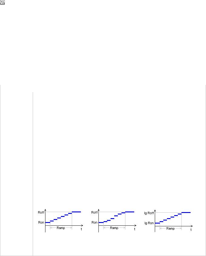
NL5 circuit simulator |
|
|
Руководство Пользователя |
|
|||
|
|
|
|
|
|
|
|
S |
|
Current controlled switch |
|
S/S_CCS_Pulse.nl5 |
|
||
|
|
|
|
|
|
|
|
|
Model |
Parameter |
Units |
Description |
|
||
|
|
|
|
|
|
|
|
|
Pulse |
Width |
s |
Pulse width. |
|
||
|
|
|
|
|
|
||
|
Threshold |
A |
Current threshold. |
|
|||
|
|
|
|
||||
|
|
|
|
|
|
|
|
|
|
|
Active |
|
Active state: Off/On. |
|
|
|
|
|
|
|
|
|
|
|
|
|
One-shot pulse generator. When increasing input current Iin crosses “Threshold” value, |
|
|||
|
|
|
switch is set to active state for “Width” time interval. If increasing Iin crosses “Threshold” value |
|
|||
|
|
|
while switch is in active state, the pulse is restarted. |
|
|||
|
|
|
|
|
|
|
|
|
|
|
|
|
|
||
S |
|
Current controlled switch |
|
S/S_CCS_Steps.nl5 |
|
||
|
|
|
|
|
|
|
|
|
Model |
Parameter |
Units |
Description |
|
||
|
|
|
|
|
|
|
|
|
Steps |
Threshold |
A |
Current threshold. |
|
||
|
|
|
|
|
|
||
|
Hysteresis |
A |
Hysteresis. |
|
|||
|
|
|
|
||||
|
|
|
|
|
|
|
|
|
|
|
Roff |
Ohm |
Off state resistance. |
|
|
|
|
|
|
|
|
|
|
|
|
|
Ron |
Ohm |
On state resistance. |
|
|
|
|
|
|
|
|
|
|
|
|
|
Slope |
|
Type of resistance change: Linear/Cos/Log. |
|
|
|
|
|
|
|
|
|
|
|
|
|
Ramp |
s |
Resistance ramp time. |
|
|
|
|
|
|
|
|
|
|
|
|
|
Steps |
|
Number of resistance steps in the ramp. |
|
|
|
|
|
|
|
|
|
|
|
|
|
IC |
|
Initial condition: Off/On. |
|
|
|
|
|
|
|
|
|
|
Switch with resistance ramping. When increasing input current Iin crosses “Threshold” plus “Hysteresis”/2 value, switch resistance starts ramping from “Roff” to “Ron”. When decreasing input current Iin crosses “Threshold” minus “Hysteresis”/2 value, switch resistance starts ramping from “Ron” to “Roff”.
Resistance is changing during “Ramp” time interval, with number of steps specified by “Steps” parameter. If “Steps” = 0, resistance is changed instantly.
“Slope” parameter specifies how resistance is changing during he ramp. The following slope types are available (“Steps” = 6):
Linear |
Cos |
Log |
When calculating DC operating point switch is set to the state specified in “IC”.
393

NL5 circuit simulator |
|
|
Руководство Пользователя |
|
|||
|
|
|
|
|
|
|
|
S |
|
Current controlled switch |
|
S/S_CCS_SubCir.nl5 |
|
||
|
|
|
|
|
|
|
|
|
Model |
Parameter |
Units |
Description |
|
||
|
|
|
|
|
|
|
|
SubCir |
File |
|
File name of subcircuit schematic. |
|
|||
|
|
|
|
|
|||
Pin1 |
|
Name of subcircuit label connected to pin 1 |
|
||||
|
|
|
|
|
|||
|
|
|
|
|
|
|
|
|
|
|
Pin2 |
|
Name of subcircuit label connected to pin 2 |
|
|
|
|
|
|
|
|
|
|
|
|
|
Pin3 |
|
Name of subcircuit label connected to pin 3 |
|
|
|
|
|
|
|
|
|
|
|
|
|
Pin4 |
|
Name of subcircuit label connected to pin 4 |
|
|
|
|
|
|
|
|
|
|
|
|
|
Cmd |
|
Subcircuit start-up command string |
|
|
|
|
|
|
|
|
|
|
|
|
|
IC |
|
Subcircuit Initial conditions string |
|
|
|
|
|
|
|
|
|
|
|
|
|
Subcircuit. See Working with Subcircuits chapter for details. |
|
|||
|
|
|
|
|
|
|
|
394
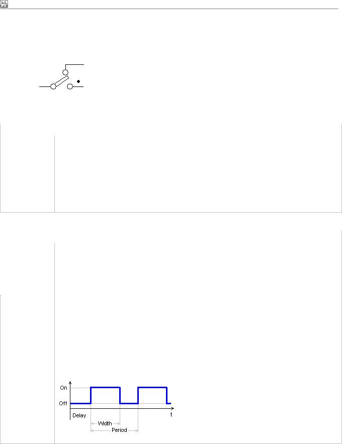
NL5 circuit simulator Руководство Пользователя
S |
|
|
SPDT switch |
|
|
|
Switch |
|
|
|||
|
|
|
|
|
|
Models |
|
Pulse |
Traces |
|
||
|
|
|
|
|
|
|
Step |
|
||||
|
|
|
|
|
|
|
List |
|
||||
|
|
|
|
|
|
|
|
|
File |
|
|
|
|
|
|
|
|
|
|
|
|
SubCir |
|
|
|
|
|
|
|
|
|
|
|
|
|
|
|
|
|
|
|
|
|
|
|
|
|
|
|
|
|
S |
|
SPDT switch |
|
|
|
|
|
|
|
S/S_SPDT_Switch_Switch.nl5 |
||
|
|
|
|
|
|
|
|
|
|
|
||
|
Model |
|
Parameter |
Units |
|
Description |
|
|
||||
|
|
|
|
|
|
|
|
|
|
|
||
Switch |
|
Switch |
|
|
|
Switch state: Off/On. |
|
|
||||
|
|
|
|
|
|
|
|
|
|
|||
|
|
|
|
|
|
|
|
|
|
|||
SPDT (single pole, double throw) switch.
Off state: “common to pin with dot” - open, “common to another pin” - closed.
On state: “common to pin with dot” - closed, “common to another pin” - open.
Open state has infinite resistance, closed state has zero resistance.
S |
|
SPDT switch |
|
|
S/S_ SPDT_Switch_Pulse.nl5 |
|
|
|
|
|
|
|
|
|
Model |
Parameter |
Units |
Description |
||
|
|
|
|
|
|
|
|
Pulse |
Period |
s |
Period. |
||
|
|
|
|
|
||
|
Width |
s |
Pulse width. |
|||
|
|
|
||||
|
|
|
|
|
|
|
|
|
|
Delay |
s |
Delay before first pulse starts. |
|
|
|
|
|
|
|
|
|
|
|
Active |
|
Active switch state: Off/On. |
|
SPDT (single pole, double throw) pulse switch.
Off state: “common to pin with dot” - open, “common to another pin” - closed.
On state: “common to pin with dot” - closed, “common to another pin” - open.
Open state has infinite resistance, closed state has zero resistance.
Switching starts after “Delay” time. Switch is in active state during “Width” time. The following switching diagram shows state of “common to dotted pin” path for “Active” = On. “Common to another pin” always has an opposite state.
395

NL5 circuit simulator |
|
|
Руководство Пользователя |
|
|||
|
|
|
|
|
|
|
|
S |
|
SPDT switch |
|
|
S/S_ SPDT_Switch_Step.nl5 |
|
|
|
|
|
|
|
|
|
|
|
Model |
Parameter |
Units |
Description |
|
||
|
|
|
|
|
|
|
|
|
Step |
Delay |
s |
Delay before active state. |
|
||
|
|
|
|
|
|
||
|
Active |
s |
Active switch state: Off/On. |
|
|||
|
|
|
|
||||
|
|
|
|
|
|
|
|
|
|
|
SPDT (single pole, double throw) step switch. |
|
|||
|
|
|
Off state: “common to pin with dot” - open, “common to another pin” - closed. |
|
|||
|
|
|
On state: “common to pin with dot” - closed, “common to another pin” - open. |
|
|||
|
|
|
Open state has infinite resistance, closed state has zero resistance. |
|
|||
|
|
|
Switch is in active state after “Delay” time. The following switching diagram shows state of |
|
|||
|
|
|
”common to dotted pin” path for “Active” = On. “Common to another pin” always has an |
|
|||
|
|
|
opposite state. |
|
|
|
|
|
|
|
|
|
|
|
|
396

NL5 circuit simulator |
|
|
Руководство Пользователя |
|
|||
|
|
|
|
|
|
|
|
S |
|
SPDT switch |
|
|
V/S_ SPDT_Switch_List.nl5 |
|
|
|
|
|
|
|
|
|
|
|
Model |
Parameter |
Units |
Description |
|
||
|
|
|
|
|
|
|
|
|
List |
List |
|
Comma-separated string. |
|
||
|
|
|
|
|
|
||
|
Cycle |
|
Cycling (repeat): No/Yes. |
|
|||
|
|
|
|
|
|||
|
|
|
|
|
|
|
|
|
|
|
Delay |
s |
Delay. |
|
|
|
|
|
|
|
|
|
|
SPDT (single pole, double throw) list switch.
Off state: “common to pin with dot” - open, “common to another pin” - closed.
On state: “common to pin with dot” - closed, “common to another pin” - open.
Open state has infinite resistance, closed state has zero resistance.
Switching sequence is defined in the “List” parameter in the csv (“comma-separated values”) format, as follows:
t0,s0,t1,s1,...,tn,sn
s0…sn defines switch state: positive number corresponds to On state, zero or negative number - Off state. If t<t0, switch is in s0 state. At t0 switch is set to s0 state. At t1 switch is set to s1 state, and so on. At t>tn, switch remains in sn state if “Cycle” parameter is set to “No”, otherwise states sequence defined in t0…tn interval is repeated continuously. In addition, the whole signal is delayed by “Delay” time.
Example:
List = 0,0,3,1,4,0,5,1,8,0
The following switching diagram shows state of ”common to dotted pin” path for “Cycle” = Yes, “Delay” = 0. “Common to another pin” always has an opposite state.
397
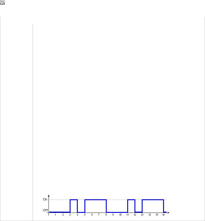
NL5 circuit simulator |
|
|
Руководство Пользователя |
|
|||
|
|
|
|
|
|
||
S |
|
SPDT switch |
|
|
V/S_ SPDT_Switch_File.nl5 |
||
|
|
|
|
|
|
|
|
|
Model |
Parameter |
Units |
Description |
|||
|
|
|
|
|
|
||
|
File |
File |
|
File name. |
|||
|
|
|
|
|
|
||
|
Cycle |
|
Cycling (repeat): No/Yes. |
||||
|
|
|
|
||||
|
|
|
|
|
|
||
|
|
|
Delay |
s |
Delay. |
||
|
|
|
|
|
|
|
|
SPDT (single pole, double throw) file switch.
Off state: “common to pin with dot” - open, “common to another pin” - closed.
On state: “common to pin with dot” - closed, “common to another pin” - open.
Open state has infinite resistance, closed state has zero resistance.
Switching sequence is defined in the text file. “File“ parameter is a file name, with full path to the file. If the file is located in the same directory as schematic file, the path can be omitted.
Switching sequence is defined in the csv (“comma-separated values”) format, as follows:
<if first line does not start with a number, it is ignored> t0,s0
t1,s1
.....
tn,sn
s0…sn defines switch state: positive number corresponds to On state, zero or negative number - Off state. If t<t0, switch is in s0 state. At t0 switch is set to s0 state. At t1 switch is set to s1 state, and so on. At t>tn, switch remains in sn state if “Cycle” parameter is set to “No”, otherwise states sequence defined in t0…tn interval is repeated continuously. In addition, the whole signal is delayed by “Delay” time.
Example:
0,0
3,1
4,0
5,1
8,0
The following switching diagram shows state of ”common to dotted pin” path for “Cycle” = Yes, “Delay” = 0. “Common to another pin” always has an opposite state.
398

NL5 circuit simulator |
|
|
Руководство Пользователя |
|
|||
|
|
|
|
|
|
|
|
S |
|
SPDT switch |
|
|
|
|
|
|
|
|
|
|
|
|
|
|
Model |
Parameter |
Units |
Description |
|
||
|
|
|
|
|
|
|
|
SubCir |
File |
|
File name of subcircuit schematic. |
|
|||
|
|
|
|
|
|||
Pin1 |
|
Name of subcircuit label connected to pin 1 |
|
||||
|
|
|
|
|
|||
|
|
|
|
|
|
|
|
|
|
|
Pin2 |
|
Name of subcircuit label connected to pin 2 |
|
|
|
|
|
|
|
|
|
|
|
|
|
Cmd |
|
Subcircuit start-up command string |
|
|
|
|
|
|
|
|
|
|
|
|
|
IC |
|
Subcircuit Initial conditions string |
|
|
|
|
|
|
|
|
|
|
|
|
|
Subcircuit. See Working with Subcircuits chapter for details. |
|
|||
|
|
|
|
|
|
|
|
399
NL5 circuit simulator |
Руководство Пользователя |
S |
SPDT logic controlled |
switch |
Models
Switch
Pulse
Steps
SubCir
Traces
S |
|
SPDT logic controlled switch |
|
|
S/S_SPDT_LCS_Switch.nl5 |
|||
|
|
|
|
|
|
|
|
|
|
Model |
Parameter |
Units |
|
Description |
|||
|
|
|
|
|
|
|
||
Switch |
Active |
|
|
Active state: Off/On. |
||||
|
|
|
|
|
|
|||
IC |
|
|
Initial condition: Off/On. |
|||||
|
|
|
|
|
||||
|
|
|
|
|
|
|
|
|
|
|
|
Logic controlled switch. |
|
|
|||
|
|
|
Off state: “common to pin with dot” - open, “common to another pin” - closed. |
|||||
|
|
|
On state: “common to pin with dot” - closed, “common to another pin” - open. |
|||||
|
|
|
Open state has infinite resistance, closed state has zero resistance. |
|||||
|
|
|
Switch is set to active or non-active state using following rules: |
|||||
|
|
|
Vin > logical threshold . . . : |
active |
||||
|
|
|
Vin < logical threshold . . . : |
non-active |
||||
|
|
|
To see and set logical levels and threshold go to Transient | Settings, or AC | Settings, then |
|||||
|
|
|
click Advanced button. |
|
|
|
||
|
|
|
When calculating DC operating point switch is set to the state defined in “IC”. |
|||||
|
|
|
|
|
|
|
|
|
400

NL5 circuit simulator |
|
|
|
Руководство Пользователя |
|
|||
|
|
|
|
|
|
|
|
|
S |
|
SPDT logic controlled switch |
|
S/S _SPDT_LCS_Pulse.nl5 |
||||
|
|
|
|
|
|
|
|
|
|
Model |
Parameter |
Units |
|
Description |
|||
|
|
|
|
|
|
|
||
|
Pulse |
Width |
s |
|
Pulse width. |
|||
|
|
|
|
|
|
|
||
|
Active |
|
|
Active state: Off/On. |
||||
|
|
|
|
|
||||
|
|
|
|
|
|
|||
|
|
|
One-shot pulse generator. |
|||||
|
|
|
Off state: “common to pin with dot” - open, “common to another pin” - closed. |
|||||
|
|
|
On state: “common to pin with dot” - closed, “common to another pin” - open. |
|||||
|
|
|
Open state has infinite resistance, closed state has zero resistance. |
|||||
|
|
|
When increasing input voltage Vin crosses logical threshold, switch is set to active state for |
|||||
|
|
|
“Width” time interval. If increasing Vin crosses logical threshold value while switch is in active |
|||||
|
|
|
state, the pulse is restarted. |
|||||
|
|
|
To see and set logical levels and threshold go to Transient | Settings, or AC | Settings, then |
|||||
|
|
|
click Advanced button. |
|
|
|
||
|
|
|
|
|
|
|
|
|
401
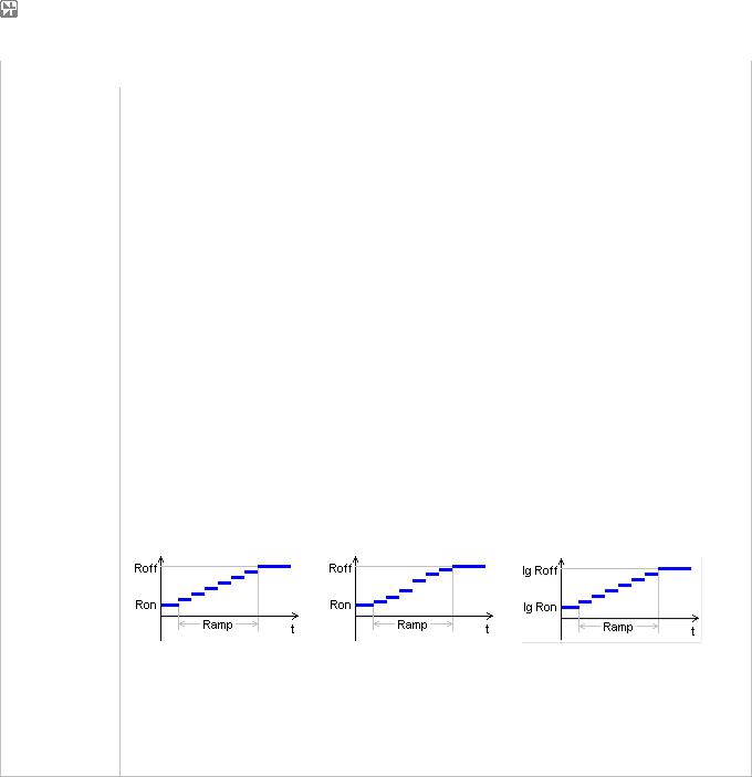
NL5 circuit simulator |
|
|
Руководство Пользователя |
|
|||
|
|
|
|
|
|
|
|
S |
|
SPDT logic controlled switch |
|
S/S_SPDT_LCS_Steps.nl5 |
|
||
|
|
|
|
|
|
|
|
|
Model |
Parameter |
Units |
Description |
|
||
|
|
|
|
|
|
|
|
|
Steps |
Roff |
Ohm |
Off state resistance. |
|
||
|
|
|
|
|
|
||
|
Ron |
Ohm |
On state resistance. |
|
|||
|
|
|
|
||||
|
|
|
|
|
|
|
|
|
|
|
Slope |
|
Type of resistance change: Linear/Cos/Log. |
|
|
|
|
|
|
|
|
|
|
|
|
|
Ramp |
s |
Resistance ramp time. |
|
|
|
|
|
|
|
|
|
|
|
|
|
Steps |
|
Number of resistance steps in the ramp. |
|
|
|
|
|
|
|
|
|
|
|
|
|
IC |
|
Initial condition: Off/On. |
|
|
|
|
|
|
|
|
|
|
Switch with resistance ramping.
When increasing input voltage Vin crosses logical threshold, resistance of “common to pin with dot” path starts ramping from “Roff” to “Ron”, resistance of “common to another pin” path starts ramping from “Ron” to “Roff”
When decreasing input voltage Vin crosses logical threshold, resistance of “common to pin with dot” path starts ramping from “Ron” to “Roff”, resistance of “common to another pin” path starts ramping from “Roff” to “Ron”
Resistance is changing during “Ramp” time interval, with number of steps specified by “Steps” parameter. If “Steps” = 0, resistance is changed instantly.
“Slope” parameter specifies how resistance is changing during he ramp. The following slope types are available (“Steps” = 6):
Linear Cos Log
To see and set logical levels and threshold go to Transient | Settings, or AC | Settings, then click Advanced button.
When calculating DC operating point switch is set to the state specified in “IC”.
402

NL5 circuit simulator |
|
|
Руководство Пользователя |
|
|||
|
|
|
|
|
|
|
|
S |
|
SPDT logic controlled switch |
|
|
|
||
|
|
|
|
|
|
|
|
|
Model |
Parameter |
Units |
Description |
|
||
|
|
|
|
|
|
|
|
SubCir |
File |
|
File name of subcircuit schematic. |
|
|||
|
|
|
|
|
|||
Pin1 |
|
Name of subcircuit label connected to pin 1 |
|
||||
|
|
|
|
|
|||
|
|
|
|
|
|
|
|
|
|
|
Pin2 |
|
Name of subcircuit label connected to pin 2 |
|
|
|
|
|
|
|
|
|
|
|
|
|
Pin3 |
|
Name of subcircuit label connected to pin 3 |
|
|
|
|
|
|
|
|
|
|
|
|
|
Pin4 |
|
Name of subcircuit label connected to pin 4 |
|
|
|
|
|
|
|
|
|
|
|
|
|
Cmd |
|
Subcircuit start-up command string |
|
|
|
|
|
|
|
|
|
|
|
|
|
IC |
|
Subcircuit Initial conditions string |
|
|
|
|
|
|
|
|
|
|
|
|
|
Subcircuit. See Working with Subcircuits chapter for details. |
|
|||
|
|
|
|
|
|
|
|
403

NL5 circuit simulator |
Руководство Пользователя |
S |
SPDT voltage |
|
Switch |
controlled switch |
|
||
|
Pulse |
||
|
|
|
|
|
|
Models |
Steps |
|
|
SubCir |
|
|
|
|
|
|
|
|
|
Views
Traces
S |
|
SPDT voltage controlled switch |
|
S/S_SPDT_VCS_Switch.nl5 |
|||
|
|
|
|
|
|
|
|
|
Model |
Parameter |
Units |
Description |
|||
|
|
|
|
|
|
||
Switch |
Threshold |
V |
Voltage threshold. |
||||
|
|
|
|
||||
Hysteresis |
V |
Hysteresis. |
|||||
|
|
|
|||||
|
|
|
|
|
|
||
|
|
|
Active |
|
Active state: Off/On. |
||
|
|
|
|
|
|
||
|
|
|
IC |
|
Initial condition: Off/On. |
||
|
|
|
|
|
|
|
|
Voltage controlled switch.
Off state: “common to pin with dot” - open, “common to another pin” - closed.
On state: “common to pin with dot” - closed, “common to another pin” - open.
Open state has infinite resistance, closed state has zero resistance.
Switch is set to active or non-active state using following rules:
Vin > Threshold + Hysteresis/2. . . |
: |
active |
Vin < Threshold - Hysteresis/2 . . . |
: |
non-active |
Otherwise . . . . . . . . . . . . . . . . . . . |
: |
previous state |
When calculating DC operating point switch is set to the state defined in “IC”.
The following is switching diagram for “common to pin with dot” path, “Active” = On:
The following switching diagram shows state of ”common to dotted pin” path for “Active” = On. “Common to another pin” always has an opposite state.
404

NL5 circuit simulator |
|
|
Руководство Пользователя |
|
|||
|
|
|
|
|
|
|
|
S |
|
SPDT voltage controlled switch |
|
S/S_SPDT _VCS_Pulse.nl5 |
|||
|
|
|
|
|
|
|
|
|
Model |
Parameter |
Units |
Description |
|||
|
|
|
|
|
|
||
|
Pulse |
Width |
s |
Pulse width. |
|||
|
|
|
|
|
|
||
|
Threshold |
V |
Voltage threshold. |
||||
|
|
|
|||||
|
|
|
|
|
|
||
|
|
|
Active |
|
Active state: Off/On. |
||
|
|
|
|
|
|
||
|
|
|
One-shot pulse generator. |
||||
|
|
|
Off state: “common to pin with dot” - open, “common to another pin” - closed. |
||||
|
|
|
On state: “common to pin with dot” - closed, “common to another pin” - open. |
||||
|
|
|
Open state has infinite resistance, closed state has zero resistance. |
||||
|
|
|
When increasing input voltage Vin crosses “Threshold” value, switch is set to active state for |
||||
|
|
|
“Width” time interval. If increasing Vin crosses “Threshold” value while switch is in active state, |
||||
|
|
|
the pulse is restarted. |
|
|
|
|
|
|
|
|
|
|
|
|
405

NL5 circuit simulator |
|
|
Руководство Пользователя |
|
|||
|
|
|
|
|
|
||
S |
|
SPDT voltage controlled switch |
|
S/S_SPDT _VCS_Steps.nl5 |
|||
|
|
|
|
|
|
|
|
|
Model |
Parameter |
Units |
Description |
|||
|
|
|
|
|
|
||
|
Steps |
Threshold |
V |
Voltage threshold. |
|||
|
|
|
|
|
|
||
|
Hysteresis |
V |
Hysteresis. |
||||
|
|
|
|||||
|
|
|
|
|
|
||
|
|
|
Roff |
Ohm |
Off state resistance. |
||
|
|
|
|
|
|
||
|
|
|
Ron |
Ohm |
On state resistance. |
||
|
|
|
|
|
|
||
|
|
|
Slope |
|
Type of resistance change: Linear/Cos/Log. |
||
|
|
|
|
|
|
||
|
|
|
Ramp |
s |
Resistance ramp time. |
||
|
|
|
|
|
|
||
|
|
|
Steps |
|
Number of resistance steps in the ramp. |
||
|
|
|
|
|
|
||
|
|
|
IC |
|
Initial condition: Off/On. |
||
|
|
|
|
|
|
|
|
Switch with resistance ramping.
When increasing input voltage Vin crosses “Threshold” plus “Hysteresis”/2 value, resistance of “common to pin with dot” path starts ramping from “Roff” to “Ron”, resistance of “common to another pin” path starts ramping from “Ron” to “Roff”.
When decreasing input voltage Vin crosses “Threshold” minus “Hysteresis”/2 value, resistance of “common to pin with dot” path starts ramping from “Ron” to “Roff”, resistance of “common to another pin” path starts ramping from “Roff” to “Ron”
Resistance is changing during “Ramp” time interval, with number of steps specified by “Steps” parameter. If “Steps” = 0, resistance is changed instantly.
“Slope” parameter specifies how resistance is changing during he ramp. The following slope types are available (“Steps” = 6):
Linear |
Cos |
Log |
When calculating DC operating point switch is set to the state specified in “IC”.
406

NL5 circuit simulator |
|
|
Руководство Пользователя |
|
|||
|
|
|
|
|
|
|
|
S |
|
SPDT voltage controlled switch |
|
|
|
||
|
|
|
|
|
|
|
|
|
Model |
Parameter |
Units |
Description |
|
||
|
|
|
|
|
|
|
|
SubCir |
File |
|
File name of subcircuit schematic. |
|
|||
|
|
|
|
|
|||
Pin1 |
|
Name of subcircuit label connected to pin 1 |
|
||||
|
|
|
|
|
|||
|
|
|
|
|
|
|
|
|
|
|
Pin2 |
|
Name of subcircuit label connected to pin 2 |
|
|
|
|
|
|
|
|
|
|
|
|
|
Pin3 |
|
Name of subcircuit label connected to pin 3 |
|
|
|
|
|
|
|
|
|
|
|
|
|
Pin4 |
|
Name of subcircuit label connected to pin 4 |
|
|
|
|
|
|
|
|
|
|
|
|
|
Cmd |
|
Subcircuit start-up command string |
|
|
|
|
|
|
|
|
|
|
|
|
|
IC |
|
Subcircuit Initial conditions string |
|
|
|
|
|
|
|
|
|
|
|
|
|
Subcircuit. See Working with Subcircuits chapter for details. |
|
|||
|
|
|
|
|
|
|
|
407
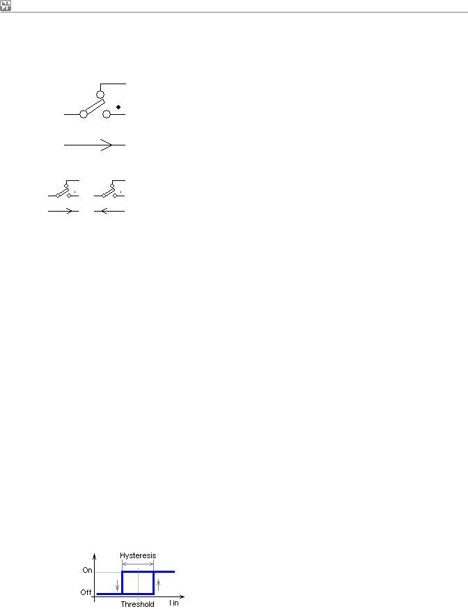
NL5 circuit simulator Руководство Пользователя
S |
|
|
SPDT current |
|
|
Switch |
|
|
||||
|
|
controlled switch |
|
|
|
|
||||||
|
|
|
|
Pulse |
|
|
||||||
|
|
|
|
|
|
|
|
|
|
|
||
|
|
|
|
|
|
|
|
Models |
Steps |
Traces |
|
|
|
|
|
|
|
|
|
|
SubCir |
|
|||
|
|
|
|
|
|
|
|
|
|
|
||
|
|
|
|
|
|
|
|
|
|
|
|
|
Views |
|
|
|
|
|
|
|
|
|
|
|
|
|
|
|
|
|
|
|
|
|
|
|
|
|
|
|
|
|
|
|
|
|
|
|
|
||
S |
|
SPDT current controlled switch |
|
|
|
|
|
S/S_SPDT _CCS_Switch.nl5 |
||||
|
|
|
|
|
|
|
|
|
|
|
||
|
|
Model |
|
Parameter |
Units |
Description |
|
|
||||
|
|
|
|
|
|
|
|
|
|
|||
|
Switch |
|
Threshold |
A |
Current threshold. |
|
|
|||||
|
|
|
|
|
|
|
|
|
|
|||
|
|
Hysteresis |
A |
Hysteresis. |
|
|
||||||
|
|
|
|
|
|
|
||||||
|
|
|
|
|
|
|
|
|
|
|||
|
|
|
|
|
Active |
|
Active state: Off/On. |
|
|
|||
|
|
|
|
|
|
|
|
|
|
|||
|
|
|
|
|
IC |
|
Initial condition: Off/On. |
|
|
|||
|
|
|
|
|
|
|
|
|
|
|
|
|
|
|
|
|
|
Current controlled switch. |
|
|
|
|
|||
|
|
|
|
|
Off state: “common to pin with dot” - open, “common to another pin” - closed. |
|||||||
|
|
|
|
|
On state: “common to pin with dot” - closed, “common to another pin” - open. |
|||||||
|
|
|
|
|
Open state has infinite resistance, closed state has zero resistance. |
|||||||
|
|
|
|
|
Switch is set to active or non-active state using following rules: |
|||||||
|
|
|
|
|
Iin > Threshold + Hysteresis/2. . . : active |
|
|
|||||
|
|
|
|
|
Iin < Threshold - Hysteresis/2 . . . : non-active |
|
|
|||||
|
|
|
|
|
Otherwise . . . . . . . . . . . . . . . . . . : previous state |
|||||||
|
|
|
|
|
When calculating DC operating point switch is set to the state defined in “IC”. |
|||||||
|
|
|
|
|
The following is switching diagram for “common to pin with dot” path, “Active” = On: |
|||||||
|
|
|
|
|
The following switching diagram shows state of ”common to dotted pin” path for “Active” = On. |
|||||||
|
|
|
|
|
“Common to another pin” always has an opposite state. |
|||||||
|
|
|
|
|
|
|
|
|
|
|
|
|
408

NL5 circuit simulator |
|
|
Руководство Пользователя |
|
|||
|
|
|
|
|
|
|
|
S |
|
SPDT current controlled switch |
|
S/S_SPDT _CCS_Pulse.nl5 |
|||
|
|
|
|
|
|
|
|
|
Model |
Parameter |
Units |
Description |
|||
|
|
|
|
|
|
||
|
Pulse |
Width |
s |
Pulse width. |
|||
|
|
|
|
|
|
||
|
Threshold |
A |
Current threshold. |
||||
|
|
|
|||||
|
|
|
|
|
|
||
|
|
|
Active |
|
Active state: Off/On. |
||
|
|
|
|
|
|
||
|
|
|
One-shot pulse generator. |
||||
|
|
|
Off state: “common to pin with dot” - open, “common to another pin” - closed. |
||||
|
|
|
On state: “common to pin with dot” - closed, “common to another pin” - open. |
||||
|
|
|
Open state has infinite resistance, closed state has zero resistance. |
||||
|
|
|
When increasing input current Iin crosses “Threshold” value, switch is set to active state for |
||||
|
|
|
“Width” time interval. If increasing Iin crosses “Threshold” value while switch is in active state, |
||||
|
|
|
the pulse is restarted. |
|
|
|
|
|
|
|
|
|
|
|
|
409
NL5 circuit simulator |
|
|
Руководство Пользователя |
|
|||
|
|
|
|
|
|
||
S |
|
SPDT current controlled switch |
|
S/S_SPDT _CCS_Steps.nl5 |
|||
|
|
|
|
|
|
|
|
|
Model |
Parameter |
Units |
Description |
|||
|
|
|
|
|
|
||
|
Steps |
Threshold |
A |
Current threshold. |
|||
|
|
|
|
|
|
||
|
Hysteresis |
A |
Hysteresis. |
||||
|
|
|
|||||
|
|
|
|
|
|
||
|
|
|
Roff |
Ohm |
Off state resistance. |
||
|
|
|
|
|
|
||
|
|
|
Ron |
Ohm |
On state resistance. |
||
|
|
|
|
|
|
||
|
|
|
Slope |
|
Type of resistance change: Linear/Cos/Log. |
||
|
|
|
|
|
|
||
|
|
|
Ramp |
s |
Resistance ramp time. |
||
|
|
|
|
|
|
||
|
|
|
Steps |
|
Number of resistance steps in the ramp. |
||
|
|
|
|
|
|
||
|
|
|
IC |
|
Initial condition: Off/On. |
||
|
|
|
|
|
|
|
|
Switch with resistance ramping.
When increasing input current Iin crosses “Threshold” plus “Hysteresis”/2 value, resistance of “common to pin with dot” path starts ramping from “Roff” to “Ron”, resistance of “common to another pin” path starts ramping from “Ron” to “Roff”.
When decreasing input current Iin crosses “Threshold” minus “Hysteresis”/2 value, resistance of “common to pin with dot” path starts ramping from “Ron” to “Roff”, resistance of “common to another pin” path starts ramping from “Roff” to “Ron”
Resistance is changing during “Ramp” time interval, with number of steps specified by “Steps” parameter. If “Steps” = 0, resistance is changed instantly.
“Slope” parameter specifies how resistance is changing during he ramp. The following slope types are available (“Steps” = 6):
Linear |
Cos |
Log |
When calculating DC operating point switch is set to the state specified in “IC”.
410

NL5 circuit simulator |
|
|
Руководство Пользователя |
|
|||
|
|
|
|
|
|
|
|
S |
|
SPDT current controlled switch |
|
|
|
||
|
|
|
|
|
|
|
|
|
Model |
Parameter |
Units |
Description |
|
||
|
|
|
|
|
|
|
|
SubCir |
File |
|
File name of subcircuit schematic. |
|
|||
|
|
|
|
|
|||
Pin1 |
|
Name of subcircuit label connected to pin 1 |
|
||||
|
|
|
|
|
|||
|
|
|
|
|
|
|
|
|
|
|
Pin2 |
|
Name of subcircuit label connected to pin 2 |
|
|
|
|
|
|
|
|
|
|
|
|
|
Pin3 |
|
Name of subcircuit label connected to pin 3 |
|
|
|
|
|
|
|
|
|
|
|
|
|
Pin4 |
|
Name of subcircuit label connected to pin 4 |
|
|
|
|
|
|
|
|
|
|
|
|
|
Cmd |
|
Subcircuit start-up command string |
|
|
|
|
|
|
|
|
|
|
|
|
|
IC |
|
Subcircuit Initial conditions string |
|
|
|
|
|
|
|
|
|
|
|
|
|
Subcircuit. See Working with Subcircuits chapter for details. |
|
|||
|
|
|
|
|
|
|
|
411

NL5 circuit simulator |
Руководство Пользователя |
T |
NPN transistor |
Models
Linear
Switch
Transistor
SubCir
Traces
 I
I
Ib
V
P = V • I
T |
|
NPN transistor |
|
|
|
|
T/T_NPN_Linear.nl5 |
|
|
|
|
|
|
|
|
|
|
|
Model |
Parameter |
Units |
Description |
|
|
|
|
|
|
|
|
|
|
|
|
|
Linear |
B |
A/A |
Gain (beta) |
|
|
|
||
|
|
|
|
|
|
|||
f1 |
Hz |
Unit gain frequency. |
|
|||||
|
|
|
|
|||||
|
|
|
|
|
|
|
||
|
|
|
IC |
A |
Initial condition: collector current. |
|
||
|
|
|
|
|
|
|||
|
|
|
Linear BJT transistor. Current controlled current source with specified bandwidth. “B” is open |
|||||
|
|
|
loop gain (beta). Frequency response consists of one pole, “f1” is unit gain frequency. “B” and |
|||||
|
|
|
“f1” can be set to infinity (“inf”). |
|
|
|
||
|
|
|
When calculating DC operating point, if “f1” is not infinity and “IC” is defined, collector current |
|||||
|
|
|
is set to specified output current “IC”. If “IC” is blank, static characteristic is used. |
|||||
|
|
|
Equivalent schematic |
Static characteristic |
AC response |
|||
|
|
|
|
|
|
|
|
|
412

NL5 circuit simulator |
|
|
Руководство Пользователя |
|
|||
|
|
|
|
|
|
|
|
T |
|
NPN transistor |
|
|
T/T_NPN_Switch.nl5 |
|
|
|
|
|
|
|
|
|
|
|
Model |
Parameter |
Units |
Description |
|
||
|
|
|
|
|
|
|
|
Switch |
Vbe |
V |
Forward voltage drop of base-emitter diode. |
|
|||
|
|
|
|
|
|||
IC |
|
Initial condition of base-emitter diode: Off/On. |
|
||||
|
|
|
|
|
|||
|
|
|
|
|
|
|
|
|
|
|
BJT transistor switch. Current controlled switch with a base-emitter diode. Switch is closed if |
|
|||
|
|
|
diode current is non-zero. |
|
|||
|
|
|
When calculating DC operating point the diode is set to the state specified in “IC”. |
|
|||
|
|
|
|
Equivalent schematic |
|
||
|
|
|
|
|
|
|
|
413

NL5 circuit simulator |
|
|
|
|
Руководство Пользователя |
|
|||
|
|
|
|
|
|
|
|
|
|
T |
|
NPN transistor |
|
|
|
|
T/T_NPN_Transistor.nl5 |
|
|
|
|
|
|
|
|
|
|
|
|
|
Model |
Parameter |
Units |
Description |
|
||||
|
|
|
|
|
|
|
|
|
|
Transistor |
B |
A/A |
Gain (beta) |
|
|||||
|
|
|
|
|
|
|
|||
f1 |
Hz |
Unit gain frequency. |
|
||||||
|
|
|
|
||||||
|
|
|
|
|
|
|
|
|
|
|
|
|
Vbe |
V |
Forward voltage drop of base-emitter diode. |
|
|||
|
|
|
|
|
|
|
|
|
|
|
|
|
Vsat |
V |
Collector-emitter saturation voltage drop. |
|
|||
|
|
|
|
|
|
|
|
|
|
|
|
|
IC |
A |
Initial condition: collector current. |
|
|||
|
|
|
|
|
|
|
|
|
|
|
|
|
ICbe |
|
Initial condition of base-emitter diode: Off/On. |
|
|||
|
|
|
|
|
|
|
|
|
|
|
|
|
ICbc |
|
Initial condition of base-collector diode: Off/On. |
|
|||
|
|
|
|
|
|
|
|
|
|
|
|
|
BJT transistor. Simplified Ebers-Moll BJT transistor model with saturation. It consists of two |
|
|||||
|
|
|
diodes (base-emitter and base-collector), and current source controlled by current through |
|
|||||
|
|
|
base-emitter diode with gain “alpha”: |
|
|
||||
|
|
|
|
|
|
||||
|
|
|
1 |
|
|||||
If collector-emitter voltage is higher than “Vsat”, base-collector diode is open, transistor is not saturated, and behaves as “Linear” model (current controlled current source with specified bandwidth). “B” is open loop gain (beta). Low signal frequency response consists of one pole, “f1” is unit gain frequency. “B” and “f1” can be set to infinity (“inf”).
If collector voltage drops below “Vsat”, base-collector diode is closed, and transistor is saturated: collector-emitter voltage is equal to “Vsat”.
When calculating DC operating point, if “f1” is not infinity and “IC” is defined, collector current is set to specified output current “IC”. If “IC” is blank, static characteristic is used. Base-emitter diode is set to the state specified in “ICbe”, Base-collector diode is set to the state specified in “ICbc”.
Equivalent schematic |
Non-saturated static |
Low signal AC response |
|
characteristic |
|
414

NL5 circuit simulator |
|
|
Руководство Пользователя |
|
|||
|
|
|
|
|
|
|
|
T |
|
NPN transistor |
|
|
T/T_NPN_SubCir.nl5 |
|
|
|
|
|
|
|
|
|
|
|
Model |
Parameter |
Units |
Description |
|
||
|
|
|
|
|
|
|
|
SubCir |
File |
|
File name of subcircuit schematic. |
|
|||
|
|
|
|
|
|||
Pin1 |
|
Name of subcircuit label connected to pin 1 |
|
||||
|
|
|
|
|
|||
|
|
|
|
|
|
|
|
|
|
|
Pin2 |
|
Name of subcircuit label connected to pin 2 |
|
|
|
|
|
|
|
|
|
|
|
|
|
Pin3 |
|
Name of subcircuit label connected to pin 3 |
|
|
|
|
|
|
|
|
|
|
|
|
|
Cmd |
|
Subcircuit start-up command string |
|
|
|
|
|
|
|
|
|
|
|
|
|
IC |
|
Subcircuit Initial conditions string |
|
|
|
|
|
|
|
|
|
|
|
|
|
Subcircuit. See Working with Subcircuits chapter for details. |
|
|||
|
|
|
|
|
|
|
|
415
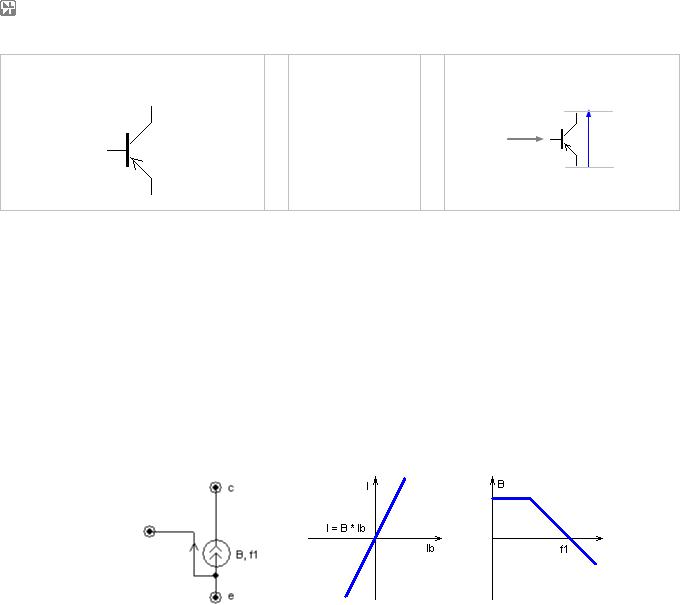
NL5 circuit simulator |
Руководство Пользователя |
T |
PNP transistor |
Models
Linear
Switch
Transistor
SubCir
Traces
 I
I
Ib
V
P = V • I
T |
|
PNP transistor |
|
|
|
|
T/T_PNP_Linear.nl5 |
|
|
|
|
|
|
|
|
|
|
|
Model |
Parameter |
Units |
Description |
|
|
|
|
|
|
|
|
|
|
|
|
|
Linear |
B |
A/A |
Gain (beta) |
|
|
|
||
|
|
|
|
|
|
|||
f1 |
Hz |
Unit gain frequency. |
|
|||||
|
|
|
|
|||||
|
|
|
|
|
|
|
||
|
|
|
IC |
A |
Initial condition: collector current. |
|
||
|
|
|
|
|
|
|||
|
|
|
Linear BJT transistor. Current controlled current source with specified bandwidth. “B” is open |
|||||
|
|
|
loop gain (beta). Frequency response consists of one pole, “f1” is unit gain frequency. “B” and |
|||||
|
|
|
“f1” can be set to infinity (“inf”). |
|
|
|
||
|
|
|
When calculating DC operating point, if “f1” is not infinity and “IC” is defined, collector current |
|||||
|
|
|
is set to specified output current “IC”. If “IC” is blank, static characteristic is used. |
|||||
|
|
|
Equivalent schematic |
Static characteristic |
AC response |
|||
|
|
|
|
|
|
|
|
|
416
NL5 circuit simulator |
|
|
Руководство Пользователя |
|
|||
|
|
|
|
|
|
|
|
T |
|
PNP transistor |
|
|
T/T_PNP_Switch.nl5 |
|
|
|
|
|
|
|
|
|
|
|
Model |
Parameter |
Units |
Description |
|
||
|
|
|
|
|
|
|
|
Switch |
Vbe |
V |
Forward voltage drop of base-emitter diode. |
|
|||
|
|
|
|
|
|||
IC |
|
Initial condition of base-emitter diode: Off/On. |
|
||||
|
|
|
|
|
|||
|
|
|
|
|
|
|
|
|
|
|
BJT transistor switch. Current controlled switch with a base-emitter diode. Switch is closed if |
|
|||
|
|
|
diode current is non-zero. |
|
|||
|
|
|
When calculating DC operating point the diode is set to the state specified in “IC”. |
|
|||
|
|
|
|
Equivalent schematic |
|
||
|
|
|
|
|
|
|
|
417
NL5 circuit simulator |
|
|
|
|
Руководство Пользователя |
|
|||
|
|
|
|
|
|
|
|
|
|
T |
|
PNP transistor |
|
|
|
|
T/T_PNP_Transistor.nl5 |
|
|
|
|
|
|
|
|
|
|
|
|
|
Model |
Parameter |
Units |
Description |
|
||||
|
|
|
|
|
|
|
|
|
|
Transistor |
B |
A/A |
Gain (beta) |
|
|||||
|
|
|
|
|
|
|
|||
f1 |
Hz |
Unit gain frequency. |
|
||||||
|
|
|
|
||||||
|
|
|
|
|
|
|
|
|
|
|
|
|
Vbe |
V |
Forward voltage drop of base-emitter diode. |
|
|||
|
|
|
|
|
|
|
|
|
|
|
|
|
Vsat |
V |
Collector-emitter saturation voltage drop. |
|
|||
|
|
|
|
|
|
|
|
|
|
|
|
|
IC |
A |
Initial condition: collector current. |
|
|||
|
|
|
|
|
|
|
|
|
|
|
|
|
ICbe |
|
Initial condition of base-emitter diode: Off/On. |
|
|||
|
|
|
|
|
|
|
|
|
|
|
|
|
ICbc |
|
Initial condition of base-collector diode: Off/On. |
|
|||
|
|
|
|
|
|
|
|
|
|
|
|
|
BJT transistor. Simplified Ebers-Moll BJT transistor model with saturation. It consists of two |
|
|||||
|
|
|
diodes (base-emitter and base-collector), and current source controlled by current through |
|
|||||
|
|
|
base-emitter diode with gain “alpha”: |
|
|
||||
|
|
|
|
|
|
||||
|
|
|
1 |
|
|||||
If collector-emitter voltage is negative and less than -“Vsat”, base-collector diode is open, transistor is not saturated, and behaves as “Linear” model (current controlled current source with specified bandwidth). “B” is open loop gain (beta). Low signal frequency response consists of one pole, “f1” is unit gain frequency. “B” and “f1” can be set to infinity (“inf”).
If collector voltage is higher than -“Vsat”, base-collector diode is closed, and transistor is saturated: collector-emitter voltage is equal to -“Vsat”.
When calculating DC operating point, if “f1” is not infinity and “IC” is defined, collector current is set to specified output current “IC”. If “IC” is blank, static characteristic is used. Base-emitter diode is set to the state specified in “ICbe”. Base-collector diode is set to the state specified in “ICbc”.
Equivalent schematic |
Non-saturated static |
Low signal AC response |
|
characteristic |
|
418

NL5 circuit simulator |
|
|
Руководство Пользователя |
|
|||
|
|
|
|
|
|
|
|
T |
|
PNP transistor |
|
|
T/T_PNP_SubCir.nl5 |
|
|
|
|
|
|
|
|
|
|
|
Model |
Parameter |
Units |
Description |
|
||
|
|
|
|
|
|
|
|
SubCir |
File |
|
File name of subcircuit schematic. |
|
|||
|
|
|
|
|
|||
Pin1 |
|
Name of subcircuit label connected to pin 1 |
|
||||
|
|
|
|
|
|||
|
|
|
|
|
|
|
|
|
|
|
Pin2 |
|
Name of subcircuit label connected to pin 2 |
|
|
|
|
|
|
|
|
|
|
|
|
|
Pin3 |
|
Name of subcircuit label connected to pin 3 |
|
|
|
|
|
|
|
|
|
|
|
|
|
Cmd |
|
Subcircuit start-up command string |
|
|
|
|
|
|
|
|
|
|
|
|
|
IC |
|
Subcircuit Initial conditions string |
|
|
|
|
|
|
|
|
|
|
|
|
|
Subcircuit. See Working with Subcircuits chapter for details. |
|
|||
|
|
|
|
|
|
|
|
419
NL5 circuit simulator |
Руководство Пользователя |
T
N-FET
Models
Linear
Switch
FET
SubCir
Traces
 I
I
V
Vgs
P = V • I
T |
|
N-FET |
|
|
|
|
|
T/T_NFET_Linear.nl5 |
|
|
|
|
|
|
|
|
|
|
Model |
Parameter |
Units |
|
Description |
|
||
|
|
|
|
|
|
|
|
|
Linear |
S |
A/V |
|
Slope |
|
|||
|
|
|
|
|
|
|||
f1 |
Hz |
|
Unit gain frequency. |
|
||||
|
|
|
|
|
||||
|
|
|
|
|
|
|
|
|
|
|
|
IC |
A |
|
Initial condition: drain current. |
|
|
|
|
|
|
|
|
|||
|
|
|
Linear FET transistor. Voltage controlled current source with specified bandwidth. “S” is |
|||||
|
|
|
open loop slope. Frequency response consists of one pole, “f1” is unit gain frequency. “S” and |
|||||
|
|
|
“f1” can be set to infinity (“inf”). |
|
||||
|
|
|
When calculating DC operating point, if “f1” is not infinity and “IC” is defined, drain current is |
|||||
|
|
|
set to specified output current “IC”. If “IC” is blank, static characteristic is used. |
|||||
|
|
|
Equivalent schematic |
Static characteristic |
AC response |
|||
|
|
|
|
|
|
|
|
|
420
NL5 circuit simulator |
|
|
|
Руководство Пользователя |
|
|||
|
|
|
|
|
|
|
|
|
T |
|
N-FET |
|
|
|
|
T/T_NFET_Switch.nl5 |
|
|
|
|
|
|
|
|
|
|
|
Model |
Parameter |
Units |
|
Description |
|
||
|
|
|
|
|
|
|
|
|
Switch |
Vth |
V |
|
Threshold. |
|
|||
|
|
|
|
|
|
|||
IC |
|
|
Initial condition of the switch: Off/On. |
|
||||
|
|
|
|
|
|
|||
|
|
|
|
|
|
|
||
|
|
|
FET switch. Voltage controlled switch. Switch is closed if gate-source voltage exceeds |
|
||||
|
|
|
threshold “Vth”. |
|
|
|
||
|
|
|
When calculating DC operating point switch is set to the state specified in “IC”. |
|
||||
|
|
|
Equivalent schematic |
|
|
|
||
|
|
|
|
|
|
|
|
|
421
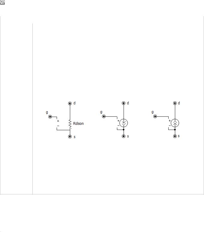
NL5 circuit simulator |
|
|
Руководство Пользователя |
|
|||
|
|
|
|
|
|
|
|
T |
|
N-FET |
|
|
|
T/T_NFET_FET.nl5 |
|
|
|
|
|
|
|
|
|
|
Model |
Parameter |
Units |
Description |
|||
|
|
|
|
|
|
||
|
FET |
S |
A/V |
Slope. |
|||
|
|
|
|
|
|
||
|
Vth |
V |
Threshold. |
||||
|
|
|
|||||
|
|
|
|
|
|
||
|
|
|
Rdson |
Ohm |
Rdson resistance. |
||
|
|
|
|
|
|
||
|
|
|
IC |
|
Initial condition: Off/R/Plus/Minus |
||
|
|
|
|
|
|
|
|
FET transistor. The model has 3 modes of operation.
1. Vgs <= Vth . . . . . . . . . . . . . . . . . . . . . . . . . . |
: I = 0 (open) |
2.Vgs > Vth, Vds <= (Vgs - Vth) * S * Rdson . . : V = I * Rdson (resistor)
3.Vgs > Vth, Vds > (Vgs - Vth) * S * Rdson . . : I = (Vgs - Vth) * S (current source)
FET works similar for positive and negative drain-source voltage, current direction changes accordingly. Equivalent schematics (Vgs > Vth):
Vds <= (Vgs-Vth)*S*Rdson |
Vds > (Vgs-Vth)*S*Rdson |
Vds > (Vgs-Vth)*S*Rdson |
|
Vds > 0 |
Vds < 0 |
When calculating DC operating point, transistor is set to an initial state specified by Initial
Condition parameter “IC” as follows:
Off . . . : |
I = 0 (open) |
|
R . . . . : |
V = I * Rdson (resistor) |
|
Plus . . : |
Vds > 0, I = (Vgs - Vth) * S |
(“positive” current source) |
Minus. : |
Vds < 0, I = (Vgs - Vth) * S |
(“negative” current source) |
T |
|
N-FET |
|
|
|
T/T_NFET_SubCir.nl5 |
|
|
|
|
|
|
|
|
Model |
Parameter |
Units |
Description |
||
|
|
|
|
|
|
|
SubCir |
File |
|
File name of subcircuit schematic. |
|||
|
|
|
|
|||
Pin1 |
|
Name of subcircuit label connected to pin 1 |
||||
|
|
|
|
|||
|
|
|
Pin2 |
|
Name of subcircuit label connected to pin 2 |
|
|
|
|
|
|
|
|
|
|
|
Pin3 |
|
Name of subcircuit label connected to pin 3 |
|
|
|
|
|
|
|
|
|
|
|
Cmd |
|
Subcircuit start-up command string |
|
|
|
|
|
|
|
|
|
|
|
IC |
|
Subcircuit Initial conditions string |
|
|
|
|
|
|
|
|
|
|
|
Subcircuit. See Working with Subcircuits chapter for details. |
|||
|
|
|
|
|
|
|
422
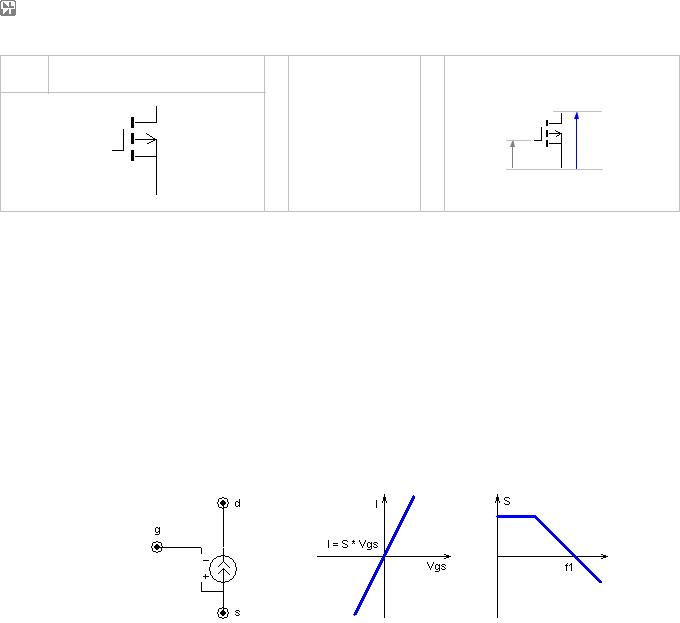
NL5 circuit simulator |
Руководство Пользователя |
T
P-FET
Models
Linear
Switch
FET
SubCir
Traces
 I
I
V
Vgs
P = V • I
T |
|
P-FET |
|
|
|
|
|
T/T_PFET_Linear.nl5 |
|
|
|
|
|
|
|
|
|
|
Model |
Parameter |
Units |
|
Description |
|
||
|
|
|
|
|
|
|
|
|
Linear |
S |
A/V |
|
Slope |
|
|||
|
|
|
|
|
|
|||
f1 |
Hz |
|
Unit gain frequency. |
|
||||
|
|
|
|
|
||||
|
|
|
|
|
|
|
|
|
|
|
|
IC |
A |
|
Initial condition: drain current. |
|
|
|
|
|
|
|
|
|||
|
|
|
Linear FET transistor. Voltage controlled current source with specified bandwidth. “S” is |
|||||
|
|
|
open loop slope. Frequency response consists of one pole, “f1” is unit gain frequency. “S” and |
|||||
|
|
|
“f1” can be set to infinity (“inf”). |
|
||||
|
|
|
When calculating DC operating point, if “f1” is not infinity and “IC” is defined, drain current is |
|||||
|
|
|
set to specified output current “IC”. If “IC” is blank, static characteristic is used. |
|||||
|
|
|
Equivalent schematic |
Static characteristic |
AC response |
|||
|
|
|
|
|
|
|
|
|
423
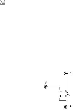
NL5 circuit simulator |
|
|
|
Руководство Пользователя |
|
|||
|
|
|
|
|
|
|
|
|
T |
|
P-FET |
|
|
|
|
T/T_PFET_Switch.nl5 |
|
|
|
|
|
|
|
|
|
|
|
Model |
Parameter |
Units |
|
Description |
|
||
|
|
|
|
|
|
|
|
|
Switch |
Vth |
V |
|
Threshold. |
|
|||
|
|
|
|
|
|
|||
IC |
|
|
Initial condition of the switch: Off/On. |
|
||||
|
|
|
|
|
|
|||
|
|
|
|
|
|
|
||
|
|
|
FET switch. Voltage controlled switch. Switch is closed if gate-source voltage is less than |
|
||||
|
|
|
threshold “Vth”. |
|
|
|
||
|
|
|
When calculating DC operating point switch is set to the state specified in “IC”. |
|
||||
|
|
|
Equivalent schematic |
|
|
|
||
|
|
|
|
|
|
|
|
|
424

NL5 circuit simulator |
|
|
Руководство Пользователя |
|
|||
|
|
|
|
|
|
|
|
T |
|
P-FET |
|
|
|
T/T_PFET_FET.nl5 |
|
|
|
|
|
|
|
|
|
|
Model |
Parameter |
Units |
Description |
|||
|
|
|
|
|
|
||
|
FET |
S |
A/V |
Slope. |
|||
|
|
|
|
|
|
||
|
Vth |
V |
Threshold. |
||||
|
|
|
|||||
|
|
|
|
|
|
||
|
|
|
Rdson |
Ohm |
Rdson resistance. |
||
|
|
|
|
|
|
||
|
|
|
IC |
|
Initial condition: Off/R/Plus/Minus |
||
|
|
|
|
|
|
|
|
FET transistor. The model has 3 modes of operation.
1.Vgs >= Vth: . . . . . . . . . . . . . . . . . . . . . . . . . . : I = 0 (open)
2.Vgs < Vth, Vds >= (Vgs - Vth) * S * Rdson . . : V = I * Rdson (resistor)
3.Vgs < Vth, Vds < (Vgs - Vth) * S * Rdson . . . : I = (Vgs - Vth) * S (current source)
FET works similar for positive and negative drain-source voltage, current direction changes accordingly. Equivalent schematics (Vgs < Vth):
Vds >= (Vgs-Vth)*S*Rdson |
Vds < (Vgs-Vth)*S*Rdson |
Vds < (Vgs-Vth)*S*Rdson |
|
Vds < 0 |
Vds > 0 |
When calculating DC operating point, transistor is set to an initial state specified by Initial
Condition parameter “IC” as follows:
Off . . . : |
I = 0 (open) |
|
R . . . . : |
V = I * Rdson (resistor) |
|
Plus . . : |
Vds < 0, I = (Vgs - Vth) * S |
(“positive” current source) |
Minus . : |
Vds > 0, I = (Vgs - Vth) * S |
(“negative” current source) |
T |
|
P-FET |
|
|
|
T/T_PFET_SubCir.nl5 |
|
|
|
|
|
|
|
|
Model |
Parameter |
Units |
Description |
||
|
|
|
|
|
|
|
SubCir |
File |
|
File name of subcircuit schematic. |
|||
|
|
|
|
|||
Pin1 |
|
Name of subcircuit label connected to pin 1 |
||||
|
|
|
|
|||
|
|
|
|
|
|
|
|
|
|
Pin2 |
|
Name of subcircuit label connected to pin 2 |
|
|
|
|
|
|
|
|
|
|
|
Pin3 |
|
Name of subcircuit label connected to pin 3 |
|
|
|
|
|
|
|
|
|
|
|
Cmd |
|
Subcircuit start-up command string |
|
|
|
|
|
|
|
|
|
|
|
IC |
|
Subcircuit Initial conditions string |
|
|
|
|
|
|
|
|
Subcircuit. See Working with Subcircuits chapter for details.
425

NL5 circuit simulator |
Руководство Пользователя |
V |
Voltage source |
Models
V
Pulse
Step
Sin
PWL
Function
File
Trace
SubCir
Traces
V
 I
I
P = V • I
V |
|
Voltage source |
|
|
V/V_VS_V.nl5 |
|
|
|
|
|
|
|
|
|
Model |
Parameter |
Units |
Description |
||
|
|
|
|
|
|
|
|
|
V |
V |
V |
Voltage. |
|
|
|
|
|
|
|
|
|
|
Constant voltage source. Voltage = “V”. |
||||
|
|
|
||||
|
|
|
|
|
|
|
426
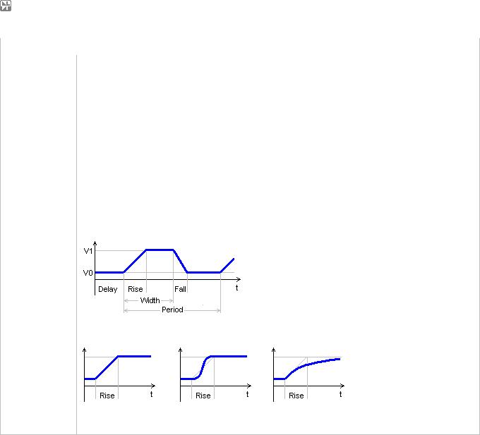
NL5 circuit simulator |
|
|
Руководство Пользователя |
|
|||
|
|
|
|
|
|
|
|
V |
|
Voltage source |
|
|
V/V_VS_Pulse.nl5 |
|
|
|
|
|
|
|
|
|
|
|
Model |
Parameter |
Units |
Description |
|
||
|
|
|
|
|
|
|
|
|
Pulse |
V1 |
V |
Pulse On voltage. |
|
||
|
|
|
|
|
|
||
|
V0 |
V |
Pulse Off voltage. |
|
|||
|
|
|
|
||||
|
|
|
|
|
|
|
|
|
|
|
Period |
s |
Period. |
|
|
|
|
|
|
|
|
|
|
|
|
|
Width |
s |
Pulse width. |
|
|
|
|
|
|
|
|
|
|
|
|
|
Slope |
|
Slope type: Linear/Cos/Exp |
|
|
|
|
|
|
|
|
|
|
|
|
|
Rise |
s |
Pulse rise length. |
|
|
|
|
|
|
|
|
|
|
|
|
|
Fall |
s |
Pulse fall length. |
|
|
|
|
|
|
|
|
|
|
|
|
|
Delay |
s |
Delay before first pulse starts. |
|
|
|
|
|
|
|
|
|
|
Pulse voltage source. Pulses start after “Delay” time. “Rise” time is included into “Width”, “Fall” time is not included into “Width”. Almost every parameter can be set to zero and infinity (“inf”), otherwise the error message will be displayed.
Slope type applies both to pulse rise and fall. The following slope types are available:
Linear |
Cos (cosine) |
Exp (exponential) |
427
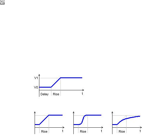
NL5 circuit simulator |
|
|
Руководство Пользователя |
|
|||
|
|
|
|
|
|
|
|
V |
|
Voltage source |
|
|
V/V_VS_Step.nl5 |
|
|
|
|
|
|
|
|
|
|
|
Model |
Parameter |
Units |
Description |
|
|
|
|
|
|
|
|
|
|
|
|
Step |
V1 |
V |
Step On voltage. |
|
|
|
|
|
|
|
|
|
||
|
V0 |
V |
Step Off voltage. |
|
|
||
|
|
|
|
|
|||
|
|
|
|
|
|
|
|
|
|
|
Slope |
s |
Slope type: Linear/Cos/Exp |
|
|
|
|
|
|
|
|
|
|
|
|
|
Rise |
s |
Step rise length. |
|
|
|
|
|
|
|
|
|
|
|
|
|
Delay |
s |
Delay before step starts. |
|
|
|
|
|
|
|
|
|
|
|
|
|
Step voltage source. Step starts after “Delay” time. |
|
|||
|
|
|
The following slope types are available: |
|
|
||
|
|
|
Linear |
|
Cos (cosine) |
Exp (exponential) |
|
|
|
|
|
|
|
|
|
428

NL5 circuit simulator |
|
|
|
Руководство Пользователя |
|
|||
|
|
|
|
|
|
|
|
|
V |
|
Voltage source |
|
|
|
V/V_VS_Sin.nl5 |
|
|
|
|
|
|
|
|
|
|
|
|
Model |
Parameter |
|
Units |
Description |
|
||
|
|
|
|
|
|
|
|
|
|
Sin |
V1 |
|
V |
Voltage amplitude. |
|
||
|
|
|
|
|
|
|
||
|
V0 |
|
V |
Voltage baseline. |
|
|||
|
|
|
|
|
||||
|
|
|
|
|
|
|
|
|
|
|
|
Period |
|
s |
Period. |
|
|
|
|
|
|
|
|
|
|
|
|
|
|
Phase |
|
deg |
Phase. |
|
|
|
|
|
|
|
|
|
|
|
|
|
|
Delay |
|
s |
Delay before sine signal starts. |
|
|
|
|
|
|
|
|
|
||
|
|
|
Sine voltage source. Sine signal starts after “Delay” time. “Phase” is sine phase in degrees |
|
||||
|
|
|
at the moment when signal starts: |
|
||||
|
|
|
|
Phase = 0 |
|
Phase = 90 |
|
|
|
|
|
If transient is paused, sine period changed, then transient is continued, the phase of the signal |
|
||||
|
|
|
remains continuous, providing smooth sine signal of variable frequency: |
|
||||
|
|
|
|
|
|
|
|
|
429
NL5 circuit simulator |
|
|
|
Руководство Пользователя |
|
||||
|
|
|
|
|
|
|
|
||
V |
|
Voltage source |
|
|
|
V/V_VS_PWL.nl5 |
|||
|
|
|
|
|
|
|
|
||
|
Model |
Parameter |
|
Units |
Description |
||||
|
|
|
|
|
|
|
|||
|
PWL |
pwl |
|
|
Comma-separated string. |
||||
|
|
|
|
|
|
|
|||
|
Cycle |
|
|
Cycling (repeat): No/Yes. |
|||||
|
|
|
|
|
|||||
|
|
|
|
|
|
|
|||
|
|
|
Delay |
|
s |
Delay. |
|||
|
|
|
|
|
|
||||
|
|
|
Piece-wise linear voltage source. Signal is defined by “pwl” parameter in the csv (“comma- |
||||||
|
|
|
separated values”) format, as follows: |
||||||
|
|
|
t0,V0,t1,V1,...,tn,Vn |
||||||
|
|
|
where all t and V can be numerical values or expressions. If t<t0, signal is V0. If t0<t<t1, signal |
||||||
|
|
|
value is linearly interpolated between V0 and V1, etc. If t>tn, then signal value is Vn if “Cycle” |
||||||
|
|
|
parameter is set to “No”, otherwise signal defined in t0…tn interval is repeated continuously. In |
||||||
|
|
|
addition, the whole signal is delayed by “Delay” time. |
||||||
|
|
|
Example: |
|
|
|
|
|
|
|
|
|
|
pwl = 0,0,1,2,4,3,5,0,8,0 |
|||||
|
|
|
If “Cycle” = Yes, “Delay” = 0, the following voltage will be generated: |
||||||
|
|
|
See Working with PWL source chapter for more details. |
||||||
|
|
|
|
|
|
|
|
||
|
|
|
|
|
|
|
|||
V |
|
Voltage source |
|
|
|
V/V_VS_Function.nl5 |
|||
|
|
|
|
|
|
|
|
||
|
Model |
Parameter |
|
Units |
Description |
||||
|
|
|
|
|
|
|
|||
Function |
F(t) |
|
V |
Function |
|||||
|
|
|
|
|
|
||||
Arbitrary function. F(t) defines voltage as a function of the following variables: |
|||||||||
|
|
|
|||||||
t - current time
V(name) - voltage on the component name I(name) - current through the component name P(name) – power on the component name
where name is the name of any component in the schematic. If F(t) is blank, voltage is zero.
Example:
F(t) = sin(t) * (1+cos(t*.01))
F(t) = V(R1) * I(R1)
Please note that V, I, and P variables are taken at previous calculation step. This may affect stability of the schematic with closed loop.
430
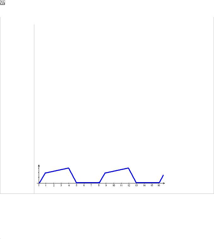
NL5 circuit simulator |
|
|
Руководство Пользователя |
|
|||
|
|
|
|
|
|
|
|
V |
|
Voltage source |
|
|
V/V_VS_File.nl5 |
|
|
|
|
|
|
|
|
|
|
|
Model |
Parameter |
Units |
Description |
|
||
|
|
|
|
|
|
|
|
|
File |
File |
|
File name. |
|
||
|
|
|
|
|
|
||
|
Cycle |
|
Cycling (repeat): No/Yes. |
|
|||
|
|
|
|
|
|||
|
|
|
|
|
|
|
|
|
|
|
Delay |
s |
Delay. |
|
|
|
|
|
|
|
|
|
|
Voltage source defined in the text file. “File“ parameter is a file name, with full path to the file. If the file is located in the same directory as schematic file, the path can be omitted. Signal is defined in following format:
<if first line does not start with a number, it is ignored> t0,V0
t1,V1
.....
tn,Vn
where all t and V can be numerical values or expressions. If t<t0, signal is V0. If t0<t<t1, signal value is linearly interpolated between V0 and V1, etc. If t>tn, then signal value is Vn if “Cycle” parameter is set to “No”, otherwise signal defined in t0…tn interval is repeated continuously. In addition, the whole signal is delayed by “Delay” time.
Example:
0,0
1,2
4,3
5,0
8,0
If “Cycle” = Yes, “Delay” = 0, the following voltage will be generated:
V |
|
Voltage source |
|
|
V/V_VS_Trace.nl5 |
|
|
|
|
|
|
|
|
|
Model |
Parameter |
Units |
Description |
||
|
|
|
|
|
|
|
|
Trace |
Trace |
|
Trace name. |
||
|
|
|
|
|
||
|
Cycle |
|
Cycling (repeat): No/Yes. |
|||
|
|
|
|
|||
|
|
|
|
|
|
|
|
|
|
Delay |
s |
Delay. |
|
|
|
|
|
|
|
|
|
|
|
Voltage source defined by a trace. “Trace” parameter is a name of the trace in the Trace list |
|||
|
|
|
(Transient/Data). Only traces loaded from data file, imported from text or binary file, |
|||
|
|
|
duplicated, or pasted from clipboard can be used for the voltage source. If “Cycle” parameter |
|||
|
|
|
is set to “Yes”, the signal is repeated continuously. In addition, the whole signal is delayed by |
|||
|
|
|
“Delay” time. |
|
|
|
|
|
|
|
|
|
|
431

NL5 circuit simulator |
|
|
Руководство Пользователя |
|
|||
|
|
|
|
|
|
|
|
V |
|
Voltage source |
|
|
V/V_VS_SubCir.nl5 |
|
|
|
|
|
|
|
|
|
|
|
Model |
Parameter |
Units |
Description |
|
||
|
|
|
|
|
|
|
|
SubCir |
File |
|
File name of subcircuit schematic. |
|
|||
|
|
|
|
|
|||
Pin1 |
|
Name of subcircuit label connected to pin 1 |
|
||||
|
|
|
|
|
|||
|
|
|
|
|
|
|
|
|
|
|
Pin2 |
|
Name of subcircuit label connected to pin 2 |
|
|
|
|
|
|
|
|
|
|
|
|
|
Cmd |
|
Subcircuit start-up command string |
|
|
|
|
|
|
|
|
|
|
|
|
|
IC |
|
Subcircuit Initial conditions string |
|
|
|
|
|
|
|
|
|
|
|
|
|
Subcircuit. See Working with Subcircuits chapter for details. |
|
|||
|
|
|
|
|
|
|
|
432
NL5 circuit simulator |
Руководство Пользователя |
V |
Voltage controlled |
|
Linear |
|
voltage source |
|
|||
|
Function |
|||
|
|
|
|
|
|
|
|
Models |
PWL |
|
|
|
VCO |
|
|
|
|
|
|
|
|
|
|
Pulse |
|
|
|
|
PWM |
|
|
|
|
SubCir |
Views |
|
|
|
|
|
|
|
|
|
|
|
|
|
|
Traces
V in |
V I |
|||
|
|
|
|
|
P = V • I |
|
|
||
V |
Voltage controlled voltage source |
|
V/V_VCVS_Linear.nl5 |
||
|
|
|
|
|
|
Model |
Parameter |
Units |
Description |
||
|
|
|
|
|
|
Linear |
K |
V/V |
Gain |
||
|
|
|
|
||
|
|
|
|
||
Linear voltage controlled voltage source. V = K * Vin.
433

NL5 circuit simulator |
|
|
Руководство Пользователя |
|
|||
|
|
|
|
|
|
|
|
V |
|
Voltage controlled voltage source |
|
V/V_VCVS_Function.nl5 |
|
||
|
|
|
|
|
|
|
|
|
Model |
Parameter |
Units |
Description |
|
||
|
|
|
|
|
|
|
|
Function |
F(x) |
V |
Output as function of the input. |
|
|||
|
|
|
|
|
|||
F(s) |
|
AC transfer function in s domain. |
|
||||
|
|
|
|
|
|||
|
|
|
|
|
|
|
|
|
|
|
IC |
V |
Initial condition: output voltage. |
|
|
|
|
|
|
|
|
|
|
Arbitrary function.
Transient analysis. F(x) defines output voltage as a function of the following variables:
x – input voltage Vin t - current time
V(name) - voltage on the component name I(name) - current through the component name P(name) – power on the component name
where name is the name of any component in the schematic. If F(x) is blank, output is zero. F(s) is ignored.
Example:
F(x) = x*x
F(x) = x * sin(t)
F(x) = P(r1)+P(r2)
Please note that input voltage x, and variables V, I, and P are taken at previous calculation step. This may affect stability of the schematic with closed loop.
AC analysis. F(s) defines transfer function in s domain. Only operators and functions that support complex numbers can be used in this function. The following variables can be used in the function:
f – current AC frequency, Hz
w – angular AC frequency, w = 2πf .
s or p – Laplace parameter, s = p = j*2πf.
z – Z-transform parameter, is defined by custom formula in the Advenced Settings dialog box.
Example:
F(s) = 1/(1+s)
F(s) = exp(-1mk*s)
F(s) is calculated at each frequency. If F(s) is blank, it is assumed to be 1. Also, if F(x) is not blank, it is linearized at DC operating point, and F(s) is multiplied by linearized gain.
When calculating DC operating point for transient or AC analysis, output is set to specified output voltage “IC”.
434

NL5 circuit simulator |
|
|
Руководство Пользователя |
|
|||
|
|
|
|
|
|
|
|
V |
|
Voltage controlled voltage source |
|
V/V_VCVS_PWL.nl5 |
|||
|
|
|
|
|
|
|
|
|
Model |
Parameter |
Units |
Description |
|||
|
|
|
|
|
|
||
|
PWL |
pwl |
|
Comma-separated string, K(Vin) |
|||
|
|
|
|
|
|
||
|
Piece-wise linear voltage controlled voltage source. Source gain K is defined by “pwl” |
||||||
|
|
|
|||||
|
|
|
string as a function of input voltage Vin. See Working with PWL model chapter for details. |
||||
|
|
|
|
|
|
|
|
|
|
|
|
|
|||
V |
|
Voltage controlled voltage source |
|
V/V_VCVS_VCO.nl5 |
|||
|
|
|
|
|
|
|
|
|
Model |
Parameter |
Units |
Description |
|||
|
|
|
|
|
|
||
|
VCO |
V1 |
V |
Voltage amplitude (Sin), or Pulse On voltage (Pulse). |
|||
|
|
|
|
|
|
||
|
V0 |
V |
Voltage baseline (Sin), or Pulse Off voltage (Pulse). |
||||
|
|
|
|||||
|
|
|
|
|
|
||
|
|
|
dFdV |
Hz/V |
Gain. |
||
|
|
|
|
|
|
||
|
|
|
Phase |
deg |
Phase. |
||
|
|
|
|
|
|
||
|
|
|
Type |
|
Signal type: Sin/Square/Triangle/Sawtooth. |
||
|
|
|
|
|
|
|
|
Voltage controlled oscillator. Output voltage is a signal with frequency equal to: f(Hz) = dFdV * Vin.
For Sine signal, “V0” is baseline, and “V1” is amplitude. For Square, Triangle, and Sawtooth signals, “V0” is Off level, “V1” is On level. “Phase” is additional phase of the signal, in degrees.
V |
|
Voltage controlled voltage source |
|
V/V_VCVS_Pulse.nl5 |
||
|
|
|
|
|
|
|
|
Model |
Parameter |
Units |
Description |
||
|
|
|
|
|
|
|
|
Pulse |
Width |
s |
Pulse width. |
||
|
|
|
|
|
||
|
Threshold |
V |
Voltage threshold. |
|||
|
|
|
||||
|
|
|
|
|
|
|
|
|
|
V1 |
V |
Pulse On voltage. |
|
|
|
|
|
|
|
|
|
|
|
V0 |
V |
Pulse Off voltage. |
|
|
|
|
|
|
|
|
|
|
|
One-shot pulse generator. When increasing input voltage Vin crosses “Threshold” value, |
|||
|
|
|
voltage pulse of “Width” duration is generated. “V0” is pulse Off level, “V1” is pulse On level. |
|||
|
|
|
If increasing Vin crosses “Threshold” value while pulse is generated, the pulse is restarted. |
|||
|
|
|
|
|
|
|
435

NL5 circuit simulator |
|
|
Руководство Пользователя |
|
|||
|
|
|
|
|
|
|
|
V |
|
Voltage controlled voltage source |
|
I/I_VCVS_PWM.nl5 |
|
||
|
|
|
|
|
|
|
|
|
Model |
Parameter |
Units |
Description |
|
||
|
|
|
|
|
|
|
|
|
PWM |
V1 |
V |
Pulse On voltage. |
|
||
|
|
|
|
|
|
||
|
V0 |
V |
Pulse Off voltage. |
|
|||
|
|
|
|
||||
|
|
|
|
|
|
|
|
|
|
|
F |
Hz |
Frequency. |
|
|
|
|
|
|
|
|
|
|
|
|
|
Phase |
deg |
Phase. |
|
|
|
|
|
|
|
|
|
|
|
|
|
Vmax |
V |
Input voltage corresponding to 100% duty. |
|
|
|
|
|
|
|
|
|
|
|
|
|
Voltage controlled Pulse-Width Modulator. Output voltage is a pulse signal of frequency “F” |
|
|||
|
|
|
shifted by “Phase”. Input voltage Vin is sampled at the beginning of each cycle of the signal, |
|
|||
|
|
|
and width of the output pulse during this cycle is calculated according to the equation: |
|
|||
|
|
|
width = 1/F * (Vin / Vmax) |
|
|||
|
|
|
or |
|
|
|
|
|
|
|
duty = 100% * (Vin / Vmax); |
|
|||
|
|
|
If the width is equal or less than zero, a short “On” pulse with the width equal to the minimum |
|
|||
|
|
|
calculation step at that moment will be generated. If the width is equal or greater than period |
|
|||
|
|
|
of frequency “F”, a short “Off” pulse at the end of the period will be generated. Due to that, the |
|
|||
|
|
|
frequency of the output signal is always “F". |
|
|||
|
|
|
|
|
|
|
|
|
|
|
|
|
|
||
V |
|
Voltage controlled voltage source |
|
V/V_VCVS_SubCir.nl5 |
|
||
|
|
|
|
|
|
|
|
|
Model |
Parameter |
Units |
Description |
|
||
|
|
|
|
|
|
|
|
SubCir |
File |
|
File name of subcircuit schematic. |
|
|||
|
|
|
|
|
|||
Pin1 |
|
Name of subcircuit label connected to pin 1 |
|
||||
|
|
|
|
|
|||
|
|
|
|
|
|
|
|
|
|
|
Pin2 |
|
Name of subcircuit label connected to pin 2 |
|
|
|
|
|
|
|
|
|
|
|
|
|
Pin3 |
|
Name of subcircuit label connected to pin 3 |
|
|
|
|
|
|
|
|
|
|
|
|
|
Pin4 |
|
Name of subcircuit label connected to pin 4 |
|
|
|
|
|
|
|
|
|
|
|
|
|
Cmd |
|
Subcircuit start-up command string |
|
|
|
|
|
|
|
|
|
|
|
|
|
IC |
|
Subcircuit Initial conditions string |
|
|
|
|
|
|
|
|
|
|
|
|
|
Subcircuit. See Working with Subcircuits chapter for details. |
|
|||
|
|
|
|
|
|
|
|
436
NL5 circuit simulator |
Руководство Пользователя |
V |
Current controlled |
|
Linear |
|
voltage source |
|
|||
|
Function |
|||
|
|
|
|
|
|
|
|
Models |
PWL |
|
|
|
CCO |
|
|
|
|
|
|
|
|
|
|
Pulse |
|
|
|
|
PWM |
|
|
|
|
SubCir |
Views |
|
|
|
|
|
|
|
|
|
|
|
|
|
|
Traces
I in |
V I |
|
P = V • I |
|
|
|
|
|
V |
Current controlled voltage source |
|
V/V_CCVS_Linear.nl5 |
||
|
|
|
|
|
|
Model |
Parameter |
Units |
Description |
||
|
|
|
|
|
|
Linear |
K |
V/A |
Gain |
||
|
|
|
|
||
|
|
|
|
||
Linear current controlled voltage source. V = K * Iin.
437

NL5 circuit simulator |
|
|
Руководство Пользователя |
|
|||
|
|
|
|
|
|
|
|
V |
|
Current controlled voltage source |
|
V/V_CCVS_Function.nl5 |
|
||
|
|
|
|
|
|
|
|
|
Model |
Parameter |
Units |
Description |
|
||
|
|
|
|
|
|
|
|
Function |
F(x) |
V |
Output as function of the input. |
|
|||
|
|
|
|
|
|||
F(s) |
|
AC transfer function in s domain. |
|
||||
|
|
|
|
|
|||
|
|
|
|
|
|
|
|
|
|
|
IC |
V |
Initial condition: output voltage. |
|
|
|
|
|
|
|
|
|
|
Arbitrary function.
Transient analysis. F(x) defines output voltage as a function of the following variables:
x – input current Iin t - current time
V(name) - voltage on the component name I(name) - current through the component name P(name) – power on the component name
where name is the name of any component in the schematic. If F(x) is blank, output is zero. F(s) is ignored.
Example:
F(x) = x*x
F(x) = x * sin(t)
F(x) = P(r1)+P(r2)
Please note that input current x, and variables V, I, and P are taken at previous calculation step. This may affect stability of the schematic with closed loop.
AC analysis. F(s) defines transfer function in s domain. Only operators and functions that support complex numbers can be used in this function. The following variables can be used in the function:
f – current AC frequency, Hz
w – angular AC frequency, w = 2πf .
s or p – Laplace parameter, s = p = j*2πf.
z – Z-transform parameter, is defined by custom formula in the Advenced Settings dialog box.
Example:
F(s) = 1/(1+s)
F(s) = exp(-1mk*s)
F(s) is calculated at each frequency. If F(s) is blank, it is assumed to be 1. Also, if F(x) is not blank, it is linearized at DC operating point, and F(s) is multiplied by linearized gain.
When calculating DC operating point for transient or AC analysis, output is set to specified output voltage “IC”.
438

NL5 circuit simulator |
|
|
Руководство Пользователя |
|
|||
|
|
|
|
|
|
|
|
V |
|
Current controlled voltage source |
|
V/V_CCVS_PWL.nl5 |
|
||
|
|
|
|
|
|
|
|
|
Model |
Parameter |
Units |
Description |
|
||
|
|
|
|
|
|
|
|
|
PWL |
pwl |
|
Comma-separated string, K(Iin) |
|
||
|
|
|
|
|
|
||
|
Piece-wise linear current controlled voltage source. Source gain K is defined by “pwl” |
|
|||||
|
|
|
|
||||
|
|
|
string as a function of input current Iin. See Working with PWL model chapter for details. |
|
|||
|
|
|
|
|
|
|
|
|
|
|
|
|
|
||
V |
|
Current controlled voltage source |
|
V/V_CCVS_CCO.nl5 |
|
||
|
|
|
|
|
|
|
|
|
Model |
Parameter |
Units |
Description |
|
||
|
|
|
|
|
|
|
|
|
CCO |
V1 |
V |
Voltage amplitude (Sin), or Pulse On voltage (Pulse). |
|
||
|
|
|
|
|
|
||
|
V0 |
V |
Voltage baseline (Sin), or Pulse Off voltage (Pulse). |
|
|||
|
|
|
|
||||
|
|
|
|
|
|
|
|
|
|
|
dFdI |
Hz/A |
Gain. |
|
|
|
|
|
|
|
|
|
|
|
|
|
Phase |
deg |
Phase. |
|
|
|
|
|
|
|
|
|
|
|
|
|
Type |
|
Signal type: Sin/Square/Triangle/Sawtooth. |
|
|
|
|
|
|
|
|
|
|
Current controlled oscillator. Output voltage is a signal with frequency equal to: f(Hz) = dFdI * Iin.
For Sine signal, “V0” is baseline, and “V1” is amplitude. For Square, Triangle, and Sawtooth signals, “V0” is Off level, “V1” is On level. “Phase” is additional phase of the signal, in degrees.
V |
|
Current controlled voltage source |
|
V/V_CCVS_Pulse.nl5 |
||
|
|
|
|
|
|
|
|
Model |
Parameter |
Units |
Description |
||
|
|
|
|
|
|
|
|
Pulse |
Width |
s |
Pulse width. |
||
|
|
|
|
|
||
|
Threshold |
A |
Current threshold. |
|||
|
|
|
||||
|
|
|
|
|
|
|
|
|
|
V1 |
V |
Pulse On voltage. |
|
|
|
|
|
|
|
|
|
|
|
V0 |
V |
Pulse Off voltage. |
|
|
|
|
|
|
|
|
|
|
|
One-shot pulse generator. When increasing input current Iin crosses “Threshold” value, |
|||
|
|
|
voltage pulse of “Width” duration is generated. “V0” is pulse Off level, “V1” is pulse On level. |
|||
|
|
|
If increasing Iin crosses “Threshold” value while pulse is generated, the pulse is restarted. |
|||
|
|
|
|
|
|
|
439
NL5 circuit simulator |
|
|
Руководство Пользователя |
|
|||
|
|
|
|
|
|
|
|
V |
|
Current controlled voltage source |
|
I/I_CCVS_PWM.nl5 |
|
||
|
|
|
|
|
|
|
|
|
Model |
Parameter |
Units |
Description |
|
||
|
|
|
|
|
|
|
|
|
PWM |
V1 |
V |
Pulse On voltage. |
|
||
|
|
|
|
|
|
||
|
V0 |
V |
Pulse Off voltage. |
|
|||
|
|
|
|
||||
|
|
|
|
|
|
|
|
|
|
|
F |
Hz |
Frequency. |
|
|
|
|
|
|
|
|
|
|
|
|
|
Phase |
deg |
Phase. |
|
|
|
|
|
|
|
|
|
|
|
|
|
Imax |
A |
Input current corresponding to 100% duty. |
|
|
|
|
|
|
|
|
|
|
|
|
|
Current controlled Pulse-Width Modulator. Output voltage is a pulse signal of frequency “F” |
|
|||
|
|
|
shifted by “Phase”. Input current Iin is sampled at the beginning of each cycle of the signal, |
|
|||
|
|
|
and width of the output pulse during this cycle is calculated according to the equation: |
|
|||
|
|
|
width = 1/F * (Iin / Imax) |
|
|||
|
|
|
or |
|
|
|
|
|
|
|
duty = 100% * (Iin / Imax); |
|
|||
|
|
|
If the width is equal or less than zero, a short “On” pulse with the width equal to the minimum |
|
|||
|
|
|
calculation step at that moment will be generated. If the width is equal or greater than period |
|
|||
|
|
|
of frequency “F”, a short “Off” pulse at the end of the period will be generated. Due to that, the |
|
|||
|
|
|
frequency of the output signal is always “F". |
|
|||
|
|
|
|
|
|
|
|
|
|
|
|
|
|
||
V |
|
Current controlled voltage source |
|
V/V_CCVS_SubCir.nl5 |
|
||
|
|
|
|
|
|
|
|
|
Model |
Parameter |
Units |
Description |
|
||
|
|
|
|
|
|
|
|
SubCir |
File |
|
File name of subcircuit schematic. |
|
|||
|
|
|
|
|
|||
Pin1 |
|
Name of subcircuit label connected to pin 1 |
|
||||
|
|
|
|
|
|||
|
|
|
|
|
|
|
|
|
|
|
Pin2 |
|
Name of subcircuit label connected to pin 2 |
|
|
|
|
|
|
|
|
|
|
|
|
|
Pin3 |
|
Name of subcircuit label connected to pin 3 |
|
|
|
|
|
|
|
|
|
|
|
|
|
Pin4 |
|
Name of subcircuit label connected to pin 4 |
|
|
|
|
|
|
|
|
|
|
|
|
|
Cmd |
|
Subcircuit start-up command string |
|
|
|
|
|
|
|
|
|
|
|
|
|
IC |
|
Subcircuit Initial conditions string |
|
|
|
|
|
|
|
|
|
|
|
|
|
Subcircuit. See Working with Subcircuits chapter for details. |
|
|||
|
|
|
|
|
|
|
|
440
NL5 circuit simulator
V |
Voltmeter |
|
Voltmeter |
|
|
|
Models |
|
Traces |
|
|
|
|
|
Руководство Пользователя
V
V |
|
Voltmeter |
|
V/V_Voltmeter_Voltmeter.nl5 |
|
|
|
|
|
|
Model |
No parameters |
||
Voltmeter |
Voltmeter. I = 0 (open circuit). |
|
441
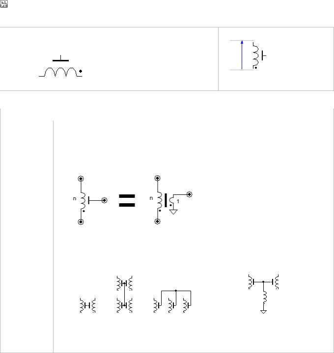
NL5 circuit simulator |
Руководство Пользователя |
W |
Winding |
|
Winding |
|
|
|
Models |
|
Traces |
|
|
|
|
|
V  I
I
P = V • I
W |
Winding |
|
|
|
W/W_Winding_Winding.nl5 |
|
|
|
|
|
|
Model |
Parameter |
Units |
Description |
||
|
|
|
|
|
|
Winding |
n |
turns |
Number of turns. |
||
|
|
|
|
||
|
|
|
|
||
Winding. The Winding is actually an ideal transformer, with 1 turn second winding, one end of each is grounded, and another end is shown as a “core” pin of the winding:
Equivalent schematic
To make an ideal transformer, connect cores of two or more windings by wire. Core magnetizing can be modeled by setting linear or non-linear inductor from core to ground:
Ideal transformers |
Transformer with |
|
magnetizing inductor |
442
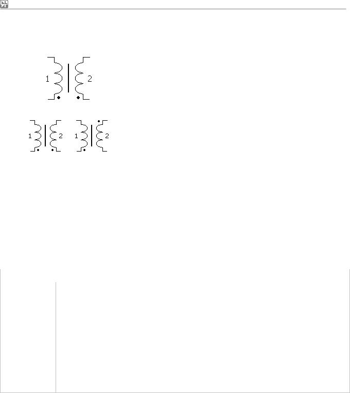
NL5 circuit simulator Руководство Пользователя
W |
|
Transformer |
|
|
Transformer |
|
|
|||||||
|
|
|
|
|
|
|
|
|
Models |
SubCir |
Traces |
|
||
|
|
|
|
|
|
|
|
|
|
|
|
|||
|
|
|
|
|
|
|
|
|
|
|
|
|
|
|
Views |
|
|
|
|
|
|
|
|
|
|
|
|
|
|
|
|
|
|
|
|
|
|
|
|
|
|
|
||
|
|
|
|
|
|
|
|
|
|
|
|
|||
W |
|
Transformer |
|
|
|
|
|
|
W/W_Transformer_Transformer.nl5 |
|||||
|
|
|
|
|
|
|
|
|
|
|
|
|||
|
|
Model |
|
|
Parameter |
Units |
Description |
|
|
|||||
|
|
|
|
|
||||||||||
Transformer |
n1 |
turns |
Number of turns in the first winding. |
|||||||||||
n2 |
turns |
Number of turns in the second winding. |
||||||||||||
|
|
|
|
|
|
|||||||||
|
|
|
|
|
|
|
|
|
||||||
|
|
|
|
|
|
Ideal transformer with 2 windings. Coupling coefficient = 1. |
||||||||
|
|
|
|
|
|
|
|
|
|
|
|
|||
|
|
|
|
|
|
|
|
|
|
|
||||
W |
|
Transformer |
|
|
|
|
|
|
|
|||||
|
|
|
|
|
|
|
|
|
|
|
||||
|
|
Model |
|
Parameter |
Units |
Description |
|
|
||||||
|
|
|
|
|
|
|
|
|||||||
|
SubCir |
|
File |
|
File name of subcircuit schematic. |
|||||||||
|
|
|
|
|
|
|
|
|
|
|
||||
|
|
Pin1 |
|
Name of subcircuit label connected to pin 1 |
||||||||||
|
|
|
|
|
|
|||||||||
|
|
|
|
|
|
|
|
|||||||
|
|
|
|
|
Pin2 |
|
Name of subcircuit label connected to pin 2 |
|||||||
|
|
|
|
|
|
|
|
|||||||
|
|
|
|
|
Pin3 |
|
Name of subcircuit label connected to pin 3 |
|||||||
|
|
|
|
|
|
|
|
|||||||
|
|
|
|
|
Pin4 |
|
Name of subcircuit label connected to pin 4 |
|||||||
|
|
|
|
|
|
|
|
|||||||
|
|
|
|
|
Cmd |
|
Subcircuit start-up command string |
|||||||
|
|
|
|
|
|
|
|
|||||||
|
|
|
|
|
IC |
|
Subcircuit Initial conditions string |
|||||||
|
|
|
|
|
|
|
|
|
|
|
|
|
|
|
Subcircuit. See Working with Subcircuits chapter for details.
443
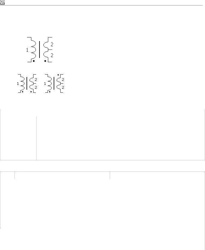
NL5 circuit simulator Руководство Пользователя
W |
|
Differential |
|
|
Transformer |
|
|
|||||
|
transformer |
|
|
|
|
|||||||
|
|
|
SubCir |
|
|
|||||||
|
|
|
|
|
|
|
Models |
Traces |
|
|||
|
|
|
|
|
|
|
|
|
|
|||
|
|
|
|
|
|
|
|
|
|
|
||
Views |
|
|
|
|
|
|
|
|
|
|
||
|
|
|
|
|
|
|
|
|
|
|
||
|
|
|
|
|
|
|
|
|
||||
W |
Differential transformer |
|
|
|
|
|
|
W/W_DifTransformer_Transformer.nl5 |
||||
|
|
|
|
|
|
|
|
|
|
|||
|
Model |
|
Parameter |
Units |
Description |
|
|
|||||
|
|
|
|
|||||||||
Transformer |
n1 |
turns |
Number of turns in the first winding. |
|||||||||
n2 |
turns |
Number of turns in the second and the third winding. |
||||||||||
|
|
|
|
|||||||||
|
|
|
|
|
|
|
|
|
|
|
|
|
Ideal differential transformer with 3 windings. Coupling coefficient = 1. Second and third windings have the same number of turns “n2”, and connected to form a differential transformer.
W Differential transformer
Model |
Parameter |
Units |
Description |
|
|
|
|
SubCir |
File |
|
File name of subcircuit schematic. |
|
|
|
|
Pin1 |
|
Name of subcircuit label connected to pin 1 |
|
|
|
||
|
|
|
|
|
Pin2 |
|
Name of subcircuit label connected to pin 2 |
|
|
|
|
|
Pin3 |
|
Name of subcircuit label connected to pin 3 |
|
|
|
|
|
Pin4 |
|
Name of subcircuit label connected to pin 4 |
|
|
|
|
|
Pin5 |
|
Name of subcircuit label connected to pin 5 |
|
|
|
|
|
Cmd |
|
Subcircuit start-up command string |
|
|
|
|
|
IC |
|
Subcircuit Initial conditions string |
|
|
|
|
|
Subcircuit. See Working with Subcircuits chapter for details. |
||
|
|
|
|
444
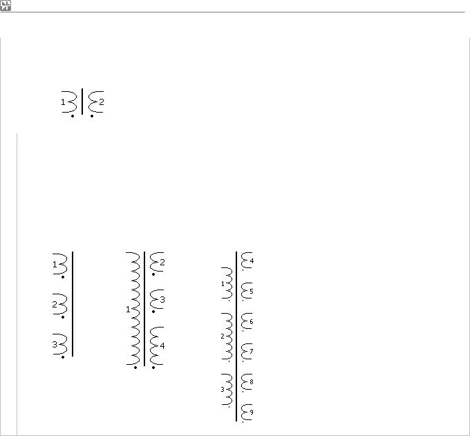
NL5 circuit simulator Руководство Пользователя
W |
Custom |
|
Transformer |
|
|
transformer |
|
|
|
||
|
Models |
SubCir |
Traces |
|
|
|
|
|
|||
|
|
|
|
||
|
|
|
|
|
|
This is a customized component. A component can be edited in the Edit Component dialog box. See |
|
Editing customized component chapter for instructions on editing a component. |
|
This component may have: |
|
- |
height from 2 to 32, |
- |
up to 9 windings (total) on both sides, |
- |
arbitrary length of a winding. |
Examples of Custom transformer component: |
|
Views |
|
445

NL5 circuit simulator |
|
|
Руководство Пользователя |
|
|||||
|
|
|
|
|
|
|
|
|
|
W |
|
Custom transformer |
|
|
W/W_CustomTransformer_Transformer.nl5 |
|
|||
|
|
|
|
|
|
|
|
|
|
|
Model |
|
Parameter |
Units |
Description |
|
|||
|
|
|
|
|
|
|
|||
Transformer |
|
n1 |
turns |
Number of turns in the first winding. |
|
||||
|
… |
… |
… |
|
|||||
|
|
|
|
|
|
||||
|
|
|
|
|
nN |
turns |
Number of turns in the Nth winding. |
|
|
|
|
|
|
|
Ideal transformer with N windings. Coupling coefficient = 1. |
|
|||
|
|
|
|
|
|
|
|
|
|
|
|
|
|
|
|
|
|
||
W |
|
Custom transformer |
|
|
|
|
|||
|
|
|
|
|
|
|
|
|
|
|
Model |
|
Parameter |
Units |
Description |
|
|||
|
|
|
|
|
|
|
|
||
SubCir |
|
File |
|
File name of subcircuit schematic. |
|
||||
|
|
|
|
|
|
|
|||
|
Pin1 |
|
Name of subcircuit label connected to pin 1 |
|
|||||
|
|
|
|
|
|
||||
|
|
|
|
|
|
|
|
||
|
|
|
|
… |
|
… |
|
||
|
|
|
|
PinN |
|
Name of subcircuit label connected to pin N |
|
||
|
|
|
|
|
|
|
|
||
|
|
|
|
Cmd |
|
Subcircuit start-up command string |
|
||
|
|
|
|
|
|
|
|
||
|
|
|
|
IC |
|
Subcircuit Initial conditions string |
|
||
|
|
|
|
|
|
|
|
||
|
|
|
|
Subcircuit. See Working with Subcircuits chapter for details. |
|
||||
|
|
|
|
|
|
|
|
|
|
446
NL5 circuit simulator |
Руководство Пользователя |
W
Wattmeter |
|
|
|
I |
|
Wattmeter |
|
|
|
|
|
|
|
|
|
Models |
|
Traces |
|
|
|
|
|
P = V • I |
|
|
|
|
|
 V
V
W |
Wattmeter |
|
W/W_Wattmeter_Wattmeter.nl5 |
|
|
|
|
|
Model |
No parameters |
|
Wattmeter |
Wattmeter. Short circuit between current ports, open circuit between voltage ports. Can |
|
|
|
be used to measure power in grounded or non-grounded load. |
447
NL5 circuit simulator |
Руководство Пользователя |
X
Delay
Models
Delay
SubCir
Traces
I
Vin |
V |
|
|
P = V • I
X |
|
Delay |
|
|
|
|
X/X_Delay_Delay.nl5 |
|
|
|
|
|
|
|
|
|
Model |
Parameter |
Units |
|
Description |
||
|
|
|
|
|
|
|
|
|
Delay |
t0 |
s |
|
Delay. |
||
|
|
|
|
|
|
||
|
IC |
V |
|
Initial condition: output voltage. |
|||
|
|
|
|
||||
|
|
|
|
|
|
||
|
|
|
Delay. Output voltage is equal to input voltage, delayed by delay time “t0”: |
||||
|
|
|
V( t ) = Vin( t – t0 ), |
where t is current time. |
|||
|
|
|
When calculating DC operating point, output is set to specified output voltage “IC”, or, if “IC” is |
||||
|
|
|
blank, to input voltage. Then output voltage is not changing until delay time “t0”. |
||||
|
|
|
The model allocates memory for storing delayed data only when needed, and frees it |
||||
|
|
|
immediately when possible. At transient start, an approximate amount of needed memory is |
||||
|
|
|
estimated based on calculation step, and, if it exceeds a limit specified in preferences |
||||
|
|
|
(Transient page), the warning message is displayed. |
||||
|
|
|
|
|
|
|
|
|
|
|
|
|
|
|
|
X |
|
Delay |
|
|
|
|
|
|
|
|
|
|
|
||
|
Model |
Parameter |
Units |
|
Description |
||
|
|
|
|
|
|
|
|
SubCir |
File |
|
|
File name of subcircuit schematic. |
|||
|
|
|
|
|
|||
Pin1 |
|
|
Name of subcircuit label connected to pin 1 |
||||
|
|
|
|
|
|||
|
|
|
|
|
|
|
|
|
|
|
Pin2 |
|
|
Name of subcircuit label connected to pin 2 |
|
|
|
|
|
|
|
|
|
|
|
|
Cmd |
|
|
Subcircuit start-up command string |
|
|
|
|
|
|
|
|
|
|
|
|
IC |
|
|
Subcircuit Initial conditions string |
|
|
|
|
|
|
|
|
|
Subcircuit. See Working with Subcircuits chapter for details.
448

NL5 circuit simulator
X |
Transmission line |
|
Line |
|
|
||
|
|
Models |
Lossy |
|
|
|
|
|
|
|
|
Руководство Пользователя
|
|
|
|
|
|
|
Traces |
Vin Iin |
|
Iout Vout |
|||
|
|
|
|
|
|
|
|
|
|
|
|
|
|
|
|
|
|
|
|
|
449
NL5 circuit simulator |
|
|
Руководство Пользователя |
|
|||
|
|
|
|
|
|
|
|
X |
|
Transmission line |
|
|
X/X_Line_Line.nl5 |
|
|
|
|
|
|
|
|
|
|
|
Model |
Parameter |
Units |
Description |
|
||
|
|
|
|
|
|
|
|
|
Line |
t0 |
s |
Delay. |
|
||
|
|
|
|
|
|
||
|
z0 |
Ohm |
Characteristic impedance. |
|
|||
|
|
|
|
||||
|
|
|
|
|
|
|
|
|
|
|
VIC |
V |
Initial condition: voltage. |
|
|
|
|
|
|
|
|
|
|
|
|
|
IIC |
A |
Initial condition: current. |
|
|
|
|
|
|
|
|
|
|
Lossless transmission line. The voltage and current in the line are represented as a superposition of forward and reflected waves, with V/I ratio in each wave equal to line characteristic impedance “z0”. V and I values of each wave are calculated based on boundary
(input and output) conditions. The line functionality can also be described by the following equations:
Vin( t ) = z0 * ( Iin( t ) – Iout( t –t0 ) )
Vout( t ) = z0 * ( Iout( t ) – Iin( t – t0 ) )
where t is current time.
Input and output are galvanically isolated: no current is flowing between input and output, and any voltage difference between input and output may exist.
When calculating DC operating point initial forward and reflected voltage and current are calculated based on the following conditions:
if “VIC” and “IIC” are blank . . . . . . . . . . : Vin = Vout, Iin = -Iout. if “VIC” is specified and “IIC” is blank . . : Vin = Vout = “VIC”.
if “VIC” is blank and “IIC” is specified . . : Iin = “IIC”, Iout = -“IIC”.
if “VIC” and “IIC” are specified . . . . . . . : Vin = Vout = “VIC”, Iin = “IIC”, Iout = -“IIC”.
The model allocates memory for storing forward and reflected wave data only when needed, and frees it immediately when possible. At transient start, an approximate amount of needed memory is estimated based on calculation step, and, if it exceeds a limit specified in preferences (Transient page), the warning message is displayed.
If real line characteristics are given in line capacitance and inductance per length, the following equations can be used to derive “t0” and “z0” parameters:
t0 = sqrt(L*C) * D
z0 = sqrt(L/C) where:
C – line capacitance per length, F/m L – line inductance per length, H/m D – line length, m
450

NL5 circuit simulator |
|
|
Руководство Пользователя |
|
|||
|
|
|
|
|
|
|
|
X |
|
Transmission line |
|
|
X/X_Line_Lossy.nl5 |
|
|
|
|
|
|
|
|
|
|
|
Model |
Parameter |
Units |
Description |
|
||
|
|
|
|
|
|
|
|
|
Lossy |
t0 |
s |
Delay. |
|
||
|
|
|
|
|
|
||
|
z0 |
Ohm |
Characteristic impedance. |
|
|||
|
|
|
|
||||
|
|
|
|
|
|
|
|
|
|
|
R |
Ohm/ns |
Series resistance per ns. |
|
|
|
|
|
|
|
|
|
|
|
|
|
fr |
MHz |
Skin losses cutoff (3 dB) frequency. |
|
|
|
|
|
|
|
|
|
|
|
|
|
G |
1/Ohm/ns |
Shunt conductance per ns. |
|
|
|
|
|
|
|
|
|
|
|
|
|
fG |
MHz |
Dielectric losses cutoff (3 dB) frequency. |
|
|
|
|
|
|
|
|
|
|
|
|
|
VIC |
V |
Initial condition: voltage. |
|
|
|
|
|
|
|
|
|
|
|
|
|
IIC |
A |
Initial condition: current. |
|
|
|
|
|
|
|
|
|
|
Lossy transmission line. Lossy line modeling is similar to lossless transmission line, with addition of losses due to series resistance, skin effect, shunt conductance, and dielectric losses.
Constant series resistance is defined by “r” parameter. Skin losses are modeled by a number of RL chains, providing series impedance increase as a square root of frequency. The number of chains is automatically optimized based on calculation step value; however, the maximum impedance increase due to skin effect is limited to 40 dB (100 times). “fr” parameter defines a frequency where effective series impedance is approximately 3 dB higher than “r”. Skin losses are calculated only if “r” > 0 and “fr is not infinite.
Constant shunt conductance is defined by “G” parameter. Dielectric losses are modeled by a shunt capacitance, providing shunt admittance increase proportional to frequency. “fG” parameter defines a frequency where effective shunt admittance is approximately 3 dB higher than “G”. Dielectric losses are calculated only if “G” > 0 and “fG is not infinite.
Input and output are galvanically isolated: no current is flowing between input and output, and any voltage difference between input and output may exist.
When calculating DC operating point initial forward and reflected voltage and current are calculated based on the following conditions:
if “VIC” and “IIC” are blank . . . . . . . . . . : Vin = Vout, Iin = -Iout. if “VIC” is specified and “IIC” is blank . . : Vin = Vout = “VIC”.
if “VIC” is blank and “IIC” is specified . . : Iin = “IIC”, Iout = -“IIC”.
if “VIC” and “IIC” are specified . . . . . . . : Vin = Vout = “VIC”, Iin = “IIC”, Iout = -“IIC”.
The model allocates all the required memory immediately at transient start. The amount of memory is proportional to line delay and inverse proportional to calculation step. If the memory required exceeds a limit specified in preferences (Transient page), the warning message is displayed.
If real line characteristics are given in line capacitance and inductance per length, the following equations can be used to derive “t0” and “z0” parameters:
t0 = sqrt(L*C) * D
z0 = sqrt(L/C) where:
C – line capacitance per length, F/m L – line inductance per length, H/m D – line length, m
451
NL5 circuit simulator |
Руководство Пользователя |
X |
Sample/Hold |
|
SH |
|
|
|
|
SubCir |
|
|
|
Models |
|
Traces |
|
|
|
|
|
I
Vin |
V |
|
P = V • I
Views
Views are used to specify type and polarity of control signal.
X |
|
Sample/Hold |
|
|
X/X_SampleHold_SH.nl5 |
|
|
|
|
|
|
|
|
|
Model |
Parameter |
Units |
Description |
||
|
|
|
|
|
|
|
|
SH |
IC |
V |
Initial condition: output voltage. |
||
|
|
|
|
|
||
|
|
|
|
|
||
Sample/hold, track/hold. Depending on view, the model is functioning as a sample/hold, or as a track/hold. In sample/hold mode, input voltage is sampled at rising or falling edge of a logical clock signal. In track/hold mode, output voltage tracks input voltage while clock signal is above the logical threshold, and holds it while clock signal is below the logical threshold (clock signal can be inverted).
To see and set logical threshold go to Transient | Settings, or AC | Settings then click
Advanced button.
A waveforms example for different modes:
When calculating DC operating point output is set to specified output voltage “IC”.
452

NL5 circuit simulator |
|
Руководство Пользователя |
|
|||
|
|
|
|
|
|
|
X |
|
Sample/Hold |
|
|
|
|
|
|
|
|
|
|
|
|
Model |
Parameter |
Units |
Description |
|
|
|
|
|
|
|
|
|
SubCir |
File |
|
File name of subcircuit schematic. |
|
||
|
|
|
|
|||
Pin1 |
|
Name of subcircuit label connected to pin 1 |
|
|||
|
|
|
|
|
||
|
|
|
|
|
|
|
|
|
|
Pin2 |
|
Name of subcircuit label connected to pin 2 |
|
|
|
|
|
|
|
|
|
|
|
Pin3 |
|
Name of subcircuit label connected to pin 3 |
|
|
|
|
|
|
|
|
|
|
|
Cmd |
|
Subcircuit start-up command string |
|
|
|
|
|
|
|
|
|
|
|
IC |
|
Subcircuit Initial conditions string |
|
|
|
|
|
|
|
|
|
|
|
Subcircuit. See Working with Subcircuits chapter for details. |
|
||
|
|
|
|
|
|
|
453
NL5 circuit simulator |
Руководство Пользователя |
X |
Directional |
|
Coupler |
|
coupler |
|
|
||
|
|
|
|
|
|
|
Models |
|
Traces |
|
|
|
|
|
Vr
I
V
Vf
P = V • I
X |
Directional coupler |
|
|
X/X_DirCoupler_Coupler.nl5 |
||
|
|
|
|
|
|
|
Model |
Parameter |
Units |
Description |
|||
|
|
|
|
|
||
Coupler |
z0 |
Ohm |
Characteristic impedance |
|||
|
|
|
|
|||
CF |
dB |
Coupling factor |
||||
|
|
|||||
|
|
|
|
|
|
|
Directional coupler is a short circuit (no insertion loss) with two output ports: forward (Vf) and reflected (Vr). Output ports are voltage sources with zero output impedance and coupling factor CF. The output voltages are calculated as follows:
Vf = K * (V + I*z0) / 2
Vr = K * (V – I*z0) / 2
where K = 10-CF/20.
All voltages are referenced to ground.
454
NL5 circuit simulator Руководство Пользователя
X |
Block-2 |
|
SubCir |
|
|
|
|
Models |
|
Traces |
|
|
|
|
|
|
|
X |
|
Block-2 |
|
|
|
X/X_Block-2_SubCir.nl5 |
|
|
|
|
|
|
|
|
Model |
Parameter |
Units |
Description |
||
|
|
|
|
|
|
|
SubCir |
File |
|
File name of subcircuit schematic. |
|||
|
|
|
|
|||
Pin1 |
|
Name of subcircuit label connected to pin 1 |
||||
|
|
|
|
|||
|
|
|
|
|
|
|
|
|
|
Pin2 |
|
Name of subcircuit label connected to pin 2 |
|
|
|
|
|
|
|
|
|
|
|
Cmd |
|
Subcircuit start-up command string |
|
|
|
|
|
|
|
|
|
|
|
IC |
|
Subcircuit Initial conditions string |
|
|
|
|
|
|
|
|
Subcircuit. See Working with Subcircuits chapter for details.
455
NL5 circuit simulator Руководство Пользователя
X |
|
Block-3 |
|
|
|
|
SubCir |
|
|
|||
|
|
|
|
|
|
Models |
|
|
|
Traces |
|
|
|
|
|
|
|
|
|
|
|
|
|
|
|
Views |
|
|
|
|
|
|
|
|
|
|
|
|
|
|
|
|
|
|
|
|
|
|
|
|
|
|
|
|
|
|
|
|
|
|
|
|
|
|
X |
|
Block-3 |
|
|
|
|
|
|
|
|
X/X_Block-3_SubCir.nl5 |
|
|
|
|
|
|
|
|
|
|
||||
|
|
Model |
Parameter |
Units |
|
Description |
||||||
|
|
|
|
|
|
|
|
|
||||
|
SubCir |
File |
|
|
|
File name of subcircuit schematic. |
||||||
|
|
|
|
|
|
|
|
|
|
|||
|
Pin1 |
|
|
|
Name of subcircuit label connected to pin 1 |
|||||||
|
|
|
|
|
|
|
||||||
|
|
|
|
|
|
|
|
|
||||
|
|
|
|
Pin2 |
|
|
|
Name of subcircuit label connected to pin 2 |
||||
|
|
|
|
|
|
|
|
|
||||
|
|
|
|
Pin3 |
|
|
|
Name of subcircuit label connected to pin 3 |
||||
|
|
|
|
|
|
|
|
|
||||
|
|
|
|
Cmd |
|
|
|
Subcircuit start-up command string |
||||
|
|
|
|
|
|
|
|
|
||||
|
|
|
|
IC |
|
|
|
Subcircuit Initial conditions string |
||||
|
|
|
|
|
|
|
||||||
|
|
|
|
Subcircuit. See Working with Subcircuits chapter for details. |
||||||||
|
|
|
|
|
|
|
|
|
|
|
|
|
456
NL5 circuit simulator Руководство Пользователя
X |
|
Block-4 |
|
|
|
|
SubCir |
|
|
|||
|
|
|
|
|
|
Models |
|
|
|
Traces |
|
|
|
|
|
|
|
|
|
|
|
|
|
|
|
Views |
|
|
|
|
|
|
|
|
|
|
|
|
|
|
|
|
|
|
|
|
|
|
|
|
|
|
|
|
|
|
|
|
|
|
|
|
|
|
X |
|
Block-4 |
|
|
|
|
|
|
|
|
X/X_Block-4_SubCir.nl5 |
|
|
|
|
|
|
|
|
|
|
||||
|
|
Model |
Parameter |
Units |
|
Description |
||||||
|
|
|
|
|
|
|
|
|
||||
|
SubCir |
File |
|
|
|
File name of subcircuit schematic. |
||||||
|
|
|
|
|
|
|
|
|
|
|||
|
Pin1 |
|
|
|
Name of subcircuit label connected to pin 1 |
|||||||
|
|
|
|
|
|
|
||||||
|
|
|
|
|
|
|
|
|
||||
|
|
|
|
Pin2 |
|
|
|
Name of subcircuit label connected to pin 2 |
||||
|
|
|
|
|
|
|
|
|
||||
|
|
|
|
Pin3 |
|
|
|
Name of subcircuit label connected to pin 3 |
||||
|
|
|
|
|
|
|
|
|
||||
|
|
|
|
Pin4 |
|
|
|
Name of subcircuit label connected to pin 4 |
||||
|
|
|
|
|
|
|
|
|
||||
|
|
|
|
Cmd |
|
|
|
Subcircuit start-up command string |
||||
|
|
|
|
|
|
|
|
|
||||
|
|
|
|
IC |
|
|
|
Subcircuit Initial conditions string |
||||
|
|
|
|
|
|
|
||||||
|
|
|
|
Subcircuit. See Working with Subcircuits chapter for details. |
||||||||
|
|
|
|
|
|
|
|
|
|
|
|
|
457

NL5 circuit simulator Руководство Пользователя
X |
|
Block-6 |
|
|
|
|
SubCir |
|
|
|||
|
|
|
|
|
|
Models |
|
|
|
Traces |
|
|
|
|
|
|
|
|
|
|
|
|
|
|
|
Views |
|
|
|
|
|
|
|
|
|
|
|
|
|
|
|
|
|
|
|
|
|
|
|
|
|
|
|
|
|
|
|
|
|
|
|
|
|
|
X |
|
Block-6 |
|
|
|
|
|
|
|
|
X/X_Block-6_SubCir.nl5 |
|
|
|
|
|
|
|
|
|
|
||||
|
|
Model |
Parameter |
Units |
|
Description |
||||||
|
|
|
|
|
|
|
|
|
||||
|
SubCir |
File |
|
|
|
File name of subcircuit schematic. |
||||||
|
|
|
|
|
|
|
|
|
|
|||
|
Pin1 |
|
|
|
Name of subcircuit label connected to pin 1 |
|||||||
|
|
|
|
|
|
|
||||||
|
|
|
|
|
|
|
|
|
||||
|
|
|
|
Pin2 |
|
|
|
Name of subcircuit label connected to pin 2 |
||||
|
|
|
|
|
|
|
|
|
||||
|
|
|
|
Pin3 |
|
|
|
Name of subcircuit label connected to pin 3 |
||||
|
|
|
|
|
|
|
|
|
||||
|
|
|
|
Pin4 |
|
|
|
Name of subcircuit label connected to pin 4 |
||||
|
|
|
|
|
|
|
|
|
||||
|
|
|
|
Pin5 |
|
|
|
Name of subcircuit label connected to pin 5 |
||||
|
|
|
|
|
|
|
|
|
||||
|
|
|
|
Pin6 |
|
|
|
Name of subcircuit label connected to pin 6 |
||||
|
|
|
|
|
|
|
|
|
||||
|
|
|
|
Cmd |
|
|
|
Subcircuit start-up command string |
||||
|
|
|
|
|
|
|
|
|
||||
|
|
|
|
IC |
|
|
|
Subcircuit Initial conditions string |
||||
|
|
|
|
|
|
|
||||||
|
|
|
|
Subcircuit. See Working with Subcircuits chapter for details. |
||||||||
|
|
|
|
|
|
|
|
|
|
|
|
|
458
|
NL5 circuit simulator |
|
|
|
|
|
|
|
Руководство Пользователя |
|
|||
|
|
|
|
|
|
|
|
|
|
|
|
|
|
X |
|
Block-8 |
|
|
|
|
SubCir |
|
|
|
|||
|
|
|
|
|
|
Models |
|
|
|
Traces |
|
|
|
|
|
|
|
|
|
|
|
|
|
|
|
|
|
Views |
|
|
|
|
|
|
|
|
|
|
|
|
|
|
|
|
|
|
|
|
|
|
|
|
|
|
|
|
|
|
|
|
|
|
|
|
|
|
|
|
|
X |
|
Block-8 |
|
|
|
|
|
|
|
|
X/X_Block-8_SubCir.nl5 |
|
|
|
|
|
|
|
|
|
|
|
|
||||
|
|
Model |
Parameter |
Units |
|
Description |
|
||||||
|
|
|
|
|
|
|
|
|
|
||||
|
SubCir |
File |
|
|
|
File name of subcircuit schematic. |
|
||||||
|
|
|
|
|
|
|
|
|
|
|
|||
|
Pin1 |
|
|
|
Name of subcircuit label connected to pin 1 |
|
|||||||
|
|
|
|
|
|
|
|
||||||
|
|
|
|
|
|
|
|
|
|
||||
|
|
|
|
Pin2 |
|
|
|
Name of subcircuit label connected to pin 2 |
|
||||
|
|
|
|
|
|
|
|
|
|
||||
|
|
|
|
Pin3 |
|
|
|
Name of subcircuit label connected to pin 3 |
|
||||
|
|
|
|
|
|
|
|
|
|
||||
|
|
|
|
Pin4 |
|
|
|
Name of subcircuit label connected to pin 4 |
|
||||
|
|
|
|
|
|
|
|
|
|
||||
|
|
|
|
Pin5 |
|
|
|
Name of subcircuit label connected to pin 5 |
|
||||
|
|
|
|
|
|
|
|
|
|
||||
|
|
|
|
Pin6 |
|
|
|
Name of subcircuit label connected to pin 6 |
|
||||
|
|
|
|
|
|
|
|
|
|
||||
|
|
|
|
Pin7 |
|
|
|
Name of subcircuit label connected to pin 7 |
|
||||
|
|
|
|
|
|
|
|
|
|
||||
|
|
|
|
Pin8 |
|
|
|
Name of subcircuit label connected to pin 8 |
|
||||
|
|
|
|
|
|
|
|
|
|
||||
|
|
|
|
Cmd |
|
|
|
Subcircuit start-up command string |
|
||||
|
|
|
|
|
|
|
|
|
|
||||
|
|
|
|
IC |
|
|
|
Subcircuit Initial conditions string |
|
||||
|
|
|
|
Subcircuit. See Working with Subcircuits chapter for details. |
|
||||||||
|
|
|
|
|
|
|
|
|
|
|
|
|
|
459
NL5 circuit simulator |
|
|
Руководство Пользователя |
|
||
|
|
|
|
|
|
|
X |
Custom block |
|
SubCir |
|
|
|
|
|
Models |
|
Traces |
|
|
|
|
|
|
|
|
|
This is a customized component. A component can be edited in the Edit Component dialog box. See Editing customized component chapter for instructions on editing a component.
This component may have:
- arbitrary size up to 32(width) X 32(height), - up to 32 pins on each side
Examples of Custom block component:
X |
|
Custom block |
|
|
X/X_CustomBlock_SubCir.nl5 |
|
|
|
|
|
|
|
|
|
Model |
Parameter |
Units |
Description |
||
|
|
|
|
|
|
|
SubCir |
File |
|
File name of subcircuit schematic. |
|||
|
|
|
|
|||
Pin1 |
|
Name of subcircuit label connected to pin 1 |
||||
|
|
|
|
|||
|
|
|
|
|
|
|
|
|
|
… |
|
… |
|
|
|
|
PinN |
|
Name of subcircuit label connected to pin N |
|
|
|
|
Cmd |
|
Subcircuit start-up command string |
|
|
|
|
|
|
|
|
|
|
|
IC |
|
Subcircuit Initial conditions string |
|
|
|
|
|
|
|
|
|
|
|
Subcircuit. See Working with Subcircuits chapter for details. |
|||
|
|
|
|
|
|
|
460
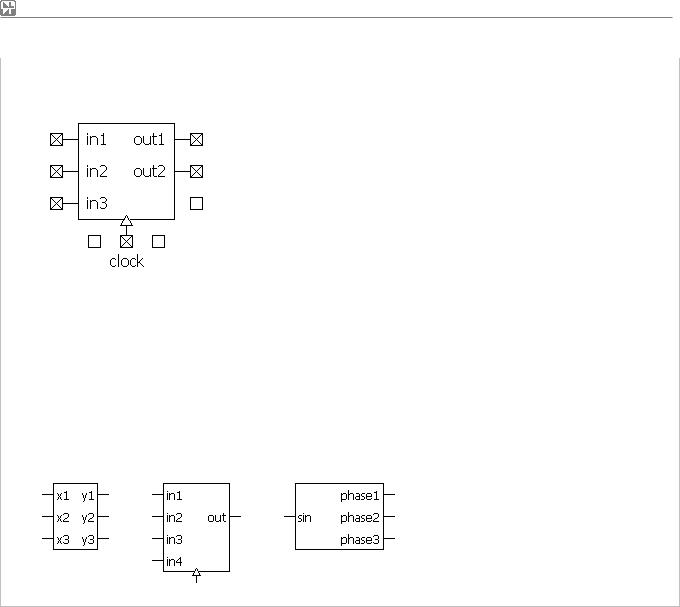
NL5 circuit simulator Руководство Пользователя
X |
Code |
|
C |
|
|
|
|
|
DLL |
|
|
|
|
Models |
|
Traces |
|
|
|
|
|
|
|
This is a customized component. A component can be edited in the Edit Component dialog box. See Editing customized component chapter for instructions on editing a component.
This component may have:
- arbitrary size up to 32(width) X 256(height),
- up to 256 inputs on the left side,
- up to 256 outputs on the right side,
- one or no clock pins on the bottom side. - custom input and output names.
Examples of Code component:
461

NL5 circuit simulator |
|
|
Руководство Пользователя |
|
|||
|
|
|
|
|
|
|
|
|
|
|
|
|
|
X/X_Code_C_Ex1.nl5 |
|
X |
|
Code |
|
|
|
X/X_Code_C_Ex2.nl5 |
|
|
|
|
|
|
|
X/X_Code_C_Ex3.nl5 |
|
|
|
|
|
|
|
|
|
|
Model |
Parameter |
Units |
Description |
|
||
|
|
|
|
|
|
|
|
|
C |
Code |
|
C-code. |
|
||
|
|
|
|
|
|
||
|
IC |
|
Initial conditions. |
|
|||
|
|
|
|
|
|||
|
|
|
|
|
|
|
|
|
|
|
C-code block. The model contains code written on simplified C language. The code will be |
|
|||
|
|
|
interpreted by NL5 during transient simulation. |
|
|||
|
|
|
“Code” contains global variables declaration, initialization code, and main code. |
|
|||
|
|
|
“IC” may contain the code assigning initial values to global variables. If not empty, “IC” code |
|
|||
|
|
|
will be executed after initialization code. |
|
|||
|
|
|
See Working with C model chapter for details of the model functionality and instructions on |
|
|||
|
|
|
creating the code. |
|
|
|
|
|
|
|
|
|
|
|
|
|
|
|
|
|
|
|
|
|
|
|
|
|
|
X/X_Code_DLL_Ex1.nl5 |
|
X |
|
Code |
|
|
|
X/X_Code_DLL_Ex2.nl5 |
|
|
|
|
|
|
|
X/X_Code_DLL_Ex3.nl5 |
|
|
|
|
|
|
|
|
|
|
Model |
Parameter |
Units |
Description |
|
||
|
|
|
|
|
|
|
|
|
DLL |
DLL |
|
DLL file name |
|
||
|
|
|
|
|
|
||
|
Init |
|
Initialization function name. |
|
|||
|
|
|
|
|
|||
|
|
|
|
|
|
|
|
|
|
|
Main |
|
Main function name. |
|
|
|
|
|
|
|
|
|
|
DLL block. Component’s code is written in C, compiled, and placed in the DLL file. DLL functions will be called by NL5 during transient simulation.
“DLL” parameter is a DLL file name, with full path to the file. If the file is located in the same directory as schematic file, the path can be omitted. File extension “dll” can be omitted.
“Init” is the name of initialization function. Initialization function is executed once at the beginning of simulation at t=0. Initialization function is optional. Leave “Init” parameter blank if initialization function is not used.
“Main” is the name of main function. If clock pin does not exist, the function is executed on every calculation step. If clock pin exists, the function is executed only on rising edge of logical clock signal.
See Working with DLL model chapter for details of the model functionality and instructions on creating code and DLL.
462

NL5 circuit simulator |
Руководство Пользователя |
Y
Logic-1
Models
Logic
Delay
Traces
V
Views
Views are used to specify inverted or non-inverted output.
Y |
|
Logic-1 |
|
|
|
Y/Y_Logic-1_Logic.nl5 |
|
|
|
|
|
|
|
|
Model |
Parameter |
Units |
Description |
||
|
|
|
|
|
|
|
|
Logic |
IC |
|
Initial condition: Low/High. |
||
|
|
|
|
|
||
|
|
|
|
|
||
Logical component with one input. Output type (inverted or non-inverted) depends on selected view.
Output voltage may have only logical levels (Low/High). Input voltage is considered Low if it is below logical threshold, or High if it is above logical threshold. To see and set logical levels and threshold go to Transient | Settings, or AC | Settings, then click Advanced button.
When calculating DC operating point output is set to specified level “IC”. When calculating transient, output voltage is always delayed by one calculation step.
Y |
|
Logic-1 |
|
|
|
Y/Y_Logic-1_Delay.nl5 |
|
|
|
|
|
|
|
|
Model |
Parameter |
Units |
Description |
||
|
|
|
|
|
|
|
|
Delay |
Delay |
s |
Output delay. |
||
|
|
|
|
|
||
|
IC |
|
Initial condition: Low/High. |
|||
|
|
|
|
|||
|
|
|
|
|
|
|
Logical component with one input and delay. Output type (inverted or non-inverted) depends on selected view.
Output voltage may have only logical levels (Low/High). Input voltage is considered Low if it is below logical threshold, or High if it is above logical threshold. To see and set logical levels and threshold go to Transient | Settings, or AC | Settings, then click Advanced button.
The output is delayed by “Delay” time. Input pulses shorter than “Delay” will not pass through and will not affect output.
When calculating DC operating point output is set to specified level “IC”.
463
NL5 circuit simulator |
Руководство Пользователя |
Y
Logic-2
Models
Logic
Delay
Traces
V
Views
Views are used to specify logical function and inverted or non-inverted output.
Y |
|
Logic-2 |
|
|
|
Y/Y_Logic-2_Logic.nl5 |
|
|
|
|
|
|
|
|
Model |
Parameter |
Units |
Description |
||
|
|
|
|
|
|
|
|
Logic |
IC |
|
Initial condition: Low/High. |
||
|
|
|
|
|
||
|
|
|
|
|
||
Logical component with two inputs. Logic function (AND, OR, XOR) and output type (inverted or non-inverted) depend on selected view.
Output voltage may have only logical levels (Low/High). Input voltage is considered Low if it is below logical threshold, or High if it is above logical threshold. To see and set logical levels and threshold go to Transient | Settings, or AC | Settings, then click Advanced button.
When calculating DC operating point output is set to specified level “IC”. When calculating transient, output voltage is always delayed by one calculation step.
Y |
|
Logic-2 |
|
|
|
Y/Y_Logic-2_Delay.nl5 |
|
|
|
|
|
|
|
|
Model |
Parameter |
Units |
Description |
||
|
|
|
|
|
|
|
|
Delay |
Delay |
s |
Output delay. |
||
|
|
|
|
|
||
|
IC |
|
Initial condition: Low/High. |
|||
|
|
|
|
|||
|
|
|
|
|
|
|
Logical component with two inputs and delay. Logic function (AND, OR, XOR) and output type (inverted or non-inverted) depend on selected view.
Output voltage may have only logical levels (Low/High). Input voltage is considered Low if it is below logical threshold, or High if it is above logical threshold. To see and set logical levels and threshold go to Transient | Settings, or AC | Settings, then click Advanced button.
The output is delayed by “Delay” time. Input pulses shorter than “Delay” will not pass through and will not affect output.
When calculating DC operating point output is set to specified level “IC”.
464
NL5 circuit simulator |
Руководство Пользователя |
Y |
Logic-3 |
|
Logic |
|
|
|
|
Delay |
|
|
|
Models |
|
Traces |
|
|
|
|
|
V
Views
Views are used to specify logical function and inverted or non-inverted output.
Y |
|
Logic-3 |
|
|
|
Y/Y_Logic-3_Logic.nl5 |
|
|
|
|
|
|
|
|
Model |
Parameter |
Units |
Description |
||
|
|
|
|
|
|
|
|
Logic |
IC |
|
Initial condition: Low/High. |
||
|
|
|
|
|
||
|
|
|
|
|
||
Logical component with three inputs. Logic function (AND, OR, XOR) and output type (inverted or non-inverted) depend on selected view.
Output voltage may have only logical levels (Low/High). Input voltage is considered Low if it is below logical threshold, or High if it is above logical threshold. To see and set logical levels and threshold go to Transient | Settings, or AC | Settings, then click Advanced button.
When calculating DC operating point output is set to specified level “IC”. When calculating transient, output voltage is always delayed by one calculation step.
465

NL5 circuit simulator |
|
|
Руководство Пользователя |
|
|||
|
|
|
|
|
|
|
|
Y |
|
Logic-3 |
|
|
|
Y/Y_Logic-3_Delay.nl5 |
|
|
|
|
|
|
|
|
|
|
Model |
Parameter |
Units |
Description |
|
||
|
|
|
|
|
|
|
|
|
Delay |
Delay |
s |
Output delay. |
|
||
|
|
|
|
|
|
||
|
IC |
|
Initial condition: Low/High. |
|
|||
|
|
|
|
|
|||
|
|
|
|
|
|
|
|
|
|
|
Logical component with three inputs and delay. Logic function (AND, OR, XOR) and |
|
|||
|
|
|
output type (inverted or non-inverted) depend on selected view. |
|
|||
|
|
|
Output voltage may have only logical levels (Low/High). Input voltage is considered Low if it is |
|
|||
|
|
|
below logical threshold, or High if it is above logical threshold. To see and set logical levels |
|
|||
|
|
|
and threshold go to Transient | Settings, or AC | Settings, then click Advanced button. |
|
|||
|
|
|
The output is delayed by “Delay” time. Input pulses shorter than “Delay” will not pass through |
|
|||
|
|
|
and will not affect output. |
|
|||
|
|
|
When calculating DC operating point output is set to specified level “IC”. |
|
|||
|
|
|
|
|
|
|
|
466
NL5 circuit simulator |
Руководство Пользователя |
Y |
Custom logic |
|
Logic |
|
|
|
|
Delay |
|
|
|
Models |
|
Traces |
|
|
|
|
|
V
Views
Views are used to specify logical function and inverted or non-inverted output.
This is a customized component. A component can be edited in the Edit Component dialog box. See Editing customized component chapter for instructions on editing a component.
This component may have:
-arbitrary size up to 32(width) X 32(height),
-up to 32 inputs on the left side,
-one output on the right side.
Y |
|
Custom logic |
|
|
Y/Y_CustomLogic_Logic.nl5 |
|
|
|
|
|
|
|
|
|
Model |
Parameter |
Units |
Description |
||
|
|
|
|
|
|
|
|
Logic |
IC |
|
Initial condition: Low/High. |
||
|
|
|
|
|
||
|
|
|
|
|
||
Custom logical component. Logic function (AND, OR, XOR) and output type (inverted or non-inverted) depend on selected view.
Output voltage may have only logical levels (Low/High). Input voltage is considered Low if it is below logical threshold, or High if it is above logical threshold. To see and set logical levels and threshold go to Transient | Settings, or AC | Settings, then click Advanced button.
When calculating DC operating point output is set to specified level “IC”. When calculating transient, output voltage is always delayed by one calculation step.
467

NL5 circuit simulator |
|
|
Руководство Пользователя |
|
|||
|
|
|
|
|
|
|
|
Y |
|
Custom logic |
|
|
Y/Y_CustomLogic_Delay.nl5 |
|
|
|
|
|
|
|
|
|
|
|
Model |
Parameter |
Units |
Description |
|
||
|
|
|
|
|
|
|
|
|
Delay |
Delay |
s |
Output delay. |
|
||
|
|
|
|
|
|
||
|
IC |
|
Initial condition: Low/High. |
|
|||
|
|
|
|
|
|||
|
|
|
|
|
|
|
|
|
|
|
Custom logical component with delay. Logic function (AND, OR, XOR) and output type |
|
|||
|
|
|
(inverted or non-inverted) depend on selected view. |
|
|||
|
|
|
Output voltage may have only logical levels (Low/High). Input voltage is considered Low if it is |
|
|||
|
|
|
below logical threshold, or High if it is above logical threshold. To see and set logical levels |
|
|||
|
|
|
and threshold go to Transient | Settings, or AC | Settings, then click Advanced button. |
|
|||
|
|
|
The output is delayed by “Delay” time. Input pulses shorter than “Delay” will not pass through |
|
|||
|
|
|
and will not affect output. |
|
|||
|
|
|
When calculating DC operating point output is set to specified level “IC”. |
|
|||
|
|
|
|
|
|
|
|
468
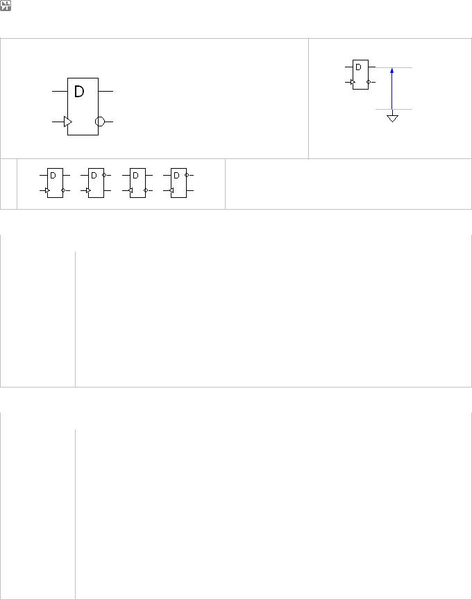
NL5 circuit simulator |
Руководство Пользователя |
Y |
D flip-flop |
|
Logic |
|
|
|
|
Delay |
|
|
|
Models |
|
Traces |
|
|
|
|
|
V
Views
Views are used to specify clock polarity and location of output pins.
Y |
|
D flip-flop |
|
|
|
Y/Y_DFlipFlop_Logic.nl5 |
|
|
|
|
|
|
|
|
|
|
Model |
Parameter |
Units |
Description |
|||
|
|
|
|
|
|
|
|
|
Logic |
|
IC |
|
Initial condition: Low/High. |
||
|
|
|
|
|
|
||
|
|
|
|
|
|
||
D flip-flop. Clock polarity (rising or falling edge) depends on selected view.
Output voltage may have only logical levels (Low/High). Input voltage is considered Low if it is below logical threshold, or High if it is above logical threshold. To see and set logical levels and threshold go to Transient | Settings, or AC | Settings, then click Advanced button.
When calculating DC operating point output is set to specified level “IC”. When calculating transient, output voltage is always delayed by one calculation step.
Y |
|
D flip-flop |
|
|
|
Y/Y_DFlipFlop_Delay.nl5 |
|
|
|
|
|
|
|
|
|
|
Model |
Parameter |
Units |
Description |
|||
|
|
|
|
|
|
|
|
|
Delay |
|
Delay |
s |
Output delay |
||
|
|
|
|
|
|
||
|
|
IC |
|
Initial condition: Low/High. |
|||
|
|
|
|
|
|||
|
|
|
|
|
|
|
|
D flip-flop with delay. Clock polarity (rising or falling edge) depends on selected view.
Output voltage may have only logical levels (Low/High). Input voltage is considered Low if it is below logical threshold, or High if it is above logical threshold. To see and set logical levels and threshold go to Transient | Settings, or AC | Settings, then click Advanced button.
Flip-flop outputs are delayed by “Delay” time. Output pulses with duration shorter than “Delay” will not show up.
When calculating DC operating point output is set to specified level “IC”.
469
NL5 circuit simulator |
Руководство Пользователя |
Y |
SR trigger |
|
Logic |
|
|
|
|
Delay |
|
|
|
Models |
|
Traces |
|
|
|
|
|
V
Views are used to specify clock and S/R inputs polarity and location of output pins.
Views
Y |
|
SR trigger |
|
|
|
Y/Y_SRTrigger_Logic.nl5 |
|
|
|
|
|
|
|
|
|
|
Model |
Parameter |
Units |
Description |
|||
|
|
|
|
|
|
|
|
|
Logic |
|
IC |
|
Initial condition: Low/High. |
||
|
|
|
|
|
|
||
|
|
|
|
|
|
||
SR trigger. Clock polarity (rising or falling edge) and S/R polarity (inverted or non-inverted) depend on selected view.
Output voltage may have only logical levels (Low/High). Input voltage is considered Low if it is below logical threshold, or High if it is above logical threshold. To see and set logical levels and threshold go to Transient | Settings, or AC | Settings, then click Advanced button.
When calculating DC operating point output is set to specified level “IC”. When calculating transient, output voltage is always delayed by one calculation step.
470

NL5 circuit simulator |
|
|
Руководство Пользователя |
|
||||
|
|
|
|
|
|
|
|
|
Y |
|
SR trigger |
|
|
|
Y/Y_SRTrigger_Delay.nl5 |
|
|
|
|
|
|
|
|
|
|
|
|
Model |
|
Parameter |
Units |
Description |
|
||
|
|
|
|
|
|
|
|
|
|
Delay |
|
Delay |
s |
Output delay. |
|
||
|
|
|
|
|
|
|
||
|
|
IC |
|
Initial condition: Low/High. |
|
|||
|
|
|
|
|
|
|||
|
|
|
|
|
|
|
|
|
|
|
|
|
SR trigger with delay. Clock polarity (rising or falling edge) and S/R polarity (inverted or non- |
|
|||
|
|
|
|
inverted) depend on selected view. |
|
|||
|
|
|
|
Output voltage may have only logical levels (Low/High). Input voltage is considered Low if it is |
|
|||
|
|
|
|
below logical threshold, or High if it is above logical threshold. To see and set logical levels |
|
|||
|
|
|
|
and threshold go to Transient | Settings, or AC | Settings, then click Advanced button. |
|
|||
|
|
|
|
Trigger outputs are delayed by “Delay” time. Output pulses with duration shorter than “Delay” |
|
|||
|
|
|
|
will not show up. |
|
|
|
|
|
|
|
|
When calculating DC operating point output is set to specified level “IC”. |
|
|||
|
|
|
|
|
|
|
|
|
471

NL5 circuit simulator |
Руководство Пользователя |
Y |
Schmitt trigger |
Models
Logic
Delay
Traces
Vin |
V |
||
|
|
|
|
Views
Views are used to specify inverted or non-inverted output.
Y |
|
Schmitt trigger |
|
|
Y/Y_SchmittTrigger_Logic.nl5 |
|
|
|
|
|
|
|
|
|
Model |
Parameter |
Units |
Description |
||
|
|
|
|
|
|
|
|
Logic |
Hysteresis |
V |
Hysteresis. |
||
|
|
|
|
|
||
|
IC |
|
Initial condition: Low/High. |
|||
|
|
|
|
|||
|
|
|
|
|
|
|
Schmitt trigger. Output type (inverted or non-inverted) depends on selected view.
Output voltage may have only logical levels (Low/High). To see and set logical levels and threshold go to Transient | Settings, or AC | Settings, then click Advanced button.
Output is set to Low or High level following rules (inverted output):
Vin > Threshold + Hysteresis/2 . . . : V = Low
Vin < Threshold - Hysteresis/2 . . . .: V = High
Otherwise . . . . . . . . . . . . . . . . . . . .: V = previous state
When calculating DC operating point output is set to specified level “IC”. When calculating transient, output voltage is always delayed by one calculation step.
472

NL5 circuit simulator |
|
|
Руководство Пользователя |
|
|||
|
|
|
|
|
|
|
|
Y |
|
Schmitt trigger |
|
|
Y/Y_SchmittTrigger_Delay.nl5 |
|
|
|
|
|
|
|
|
|
|
|
Model |
Parameter |
Units |
Description |
|
||
|
|
|
|
|
|
|
|
|
Delay |
Hysteresis |
V |
Hysteresis. |
|
||
|
|
|
|
|
|
||
|
Delay |
s |
Output delay |
|
|||
|
|
|
|
||||
|
|
|
|
|
|
|
|
|
|
|
IC |
|
Initial condition: Low/High. |
|
|
|
|
|
|
|
|
|
|
Schmitt trigger with delay. Output type (inverted or non-inverted) depends on selected view.
Output voltage may have only logical levels (Low/High). To see and set logical levels and threshold go to Transient | Settings, or AC | Settings, then click Advanced button.
Output is set to Low or High level following rules (inverted output):
Vin > Threshold + Hysteresis/2 . . . : V = Low
Vin < Threshold - Hysteresis/2 . . . .: V = High
Otherwise . . . . . . . . . . . . . . . . . . . .: V = previous state
Trigger outputs are delayed by “Delay” time. Output pulses with duration shorter than “Delay” will not show up.
When calculating DC operating point output is set to specified level “IC”.
473

NL5 circuit simulator |
Руководство Пользователя |
Y Logic generator
Models
V
Pulse
Step
List
File
Traces
V
Y |
|
Logic generator |
|
|
Y/Y_LogicGenerator_V.nl5 |
|
|
|
|
|
|
|
|
|
Model |
Parameter |
Units |
Description |
||
|
|
|
|
|
|
|
|
|
V |
Out |
|
Logical output: Low/High. |
|
|
|
|
|
|
|
|
|
|
Logical output. Generates constant Low or High logical output. |
||||
|
|
|
||||
|
|
|
To see and set logical levels go to Transient | Settings, or AC | Settings, then click |
|||
|
|
|
Advanced button. |
|
|
|
|
|
|
|
|
|
|
|
|
|
|
|
|
|
Y |
|
Logic generator |
|
|
Y/Y_LogicGenerator_Pulse.nl5 |
|
|
|
|
|
|
|
|
|
Model |
Parameter |
Units |
Description |
||
|
|
|
|
|
|
|
|
Pulse |
Period |
s |
Period. |
||
|
|
|
|
|
||
|
Width |
s |
Pulse width. |
|||
|
|
|
||||
|
|
|
|
|
|
|
|
|
|
Delay |
s |
Delay before first pulse starts. |
|
|
|
|
|
|
|
|
|
|
|
Active |
|
Active output state: Low/High. |
|
|
|
|
|
|
|
|
Logical pulses. Pulses start at “Delay” time. Output level is “Active” during “Width” time.
To see and set logical levels go to Transient | Settings, or AC | Settings, then click
Advanced button.
The following pulses will be generated if “Active” = On:
474
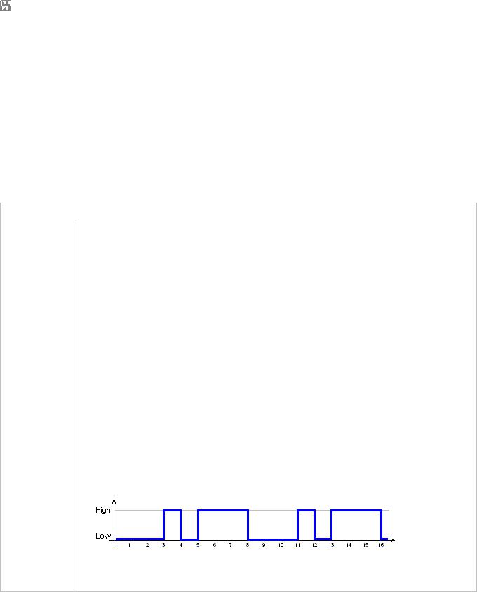
NL5 circuit simulator |
|
|
Руководство Пользователя |
|
|||
|
|
|
|
|
|
|
|
Y |
|
Logic generator |
|
|
Y/Y_LogicGenerator_Step.nl5 |
|
|
|
|
|
|
|
|
|
|
|
Model |
Parameter |
Units |
Description |
|
||
|
|
|
|
|
|
|
|
|
Step |
Delay |
s |
Delay before active state. |
|
||
|
|
|
|
|
|
||
|
Active |
|
Active output state: Low/High. |
|
|||
|
|
|
|
|
|||
|
|
|
|
|
|
|
|
|
|
|
Logical step. Output level is non-“Active” before “Delay” time, turns to “Active” level after |
|
|||
|
|
|
“Delay” time. |
|
|
|
|
|
|
|
To see and set logical levels go to Transient | Settings, or AC | Settings, then click |
|
|||
|
|
|
Advanced button. |
|
|
|
|
|
|
|
|
|
|
|
|
|
|
|
|
|
|
|
|
Y |
|
Logic generator |
|
|
Y/Y_LogicGenerator_List.nl5 |
|
|
|
|
|
|
|
|
|
|
|
Model |
Parameter |
Units |
Description |
|
||
|
|
|
|
|
|
|
|
|
List |
List |
|
Comma-separated string. |
|
||
|
|
|
|
|
|
||
|
Cycle |
|
Cycling (repeat): No/Yes. |
|
|||
|
|
|
|
|
|||
|
|
|
|
|
|
|
|
|
|
|
Delay |
s |
Delay. |
|
|
|
|
|
|
|
|
|
|
Logic list. Logical output sequence is defined in the “List” parameter in the csv (“commaseparated values”) format, as follows:
t0,s0,t1,s1,...,tn,sn
where all t and s can be numerical values or expressions. s0…sn defines output logical level: positive number corresponds to High, zero or negative number - Low. If t<t0, output level is s0. At t0 output level is s0. At t1 output level is s1, and so on. At t>tn, output remains at sn level if “Cycle” parameter is set to “No”, otherwise the sequence defined in t0…tn interval is repeated continuously. In addition, the whole signal is delayed by “Delay” time.
To see and set logical levels go to Transient | Settings, or AC | Settings, then click
Advanced button.
Example:
List = 0,0,3,1,4,0,5,1,8,0
The following logical output will be generated if “Cycle” = Yes, “Delay” = 0:
See Working with List model chapter for more details.
475
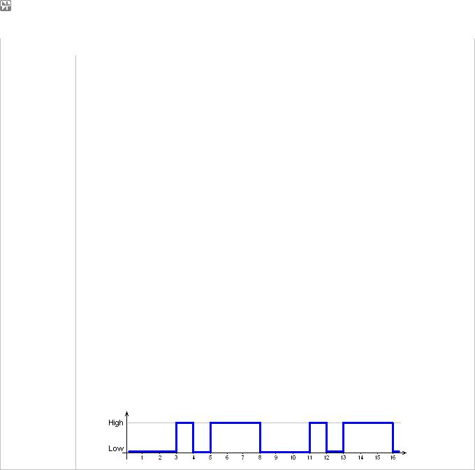
NL5 circuit simulator |
|
|
Руководство Пользователя |
|
|||
|
|
|
|
|
|
|
|
Y |
|
Logic generator |
|
|
Y/Y_LogicGenerator_File.nl5 |
|
|
|
|
|
|
|
|
|
|
|
Model |
Parameter |
Units |
Description |
|
||
|
|
|
|
|
|
|
|
|
File |
File |
|
File name. |
|
||
|
|
|
|
|
|
||
|
Cycle |
|
Cycling (repeat): No/Yes. |
|
|||
|
|
|
|
|
|||
|
|
|
|
|
|
|
|
|
|
|
Delay |
s |
Delay. |
|
|
|
|
|
|
|
|
|
|
Logic file. Logical output sequence is defined in the text file. “File“ parameter is a file name, with full path to the file. If the file is located in the same directory as schematic file, the path can be omitted. Logical output sequence is defined in the following format:
<if first line does not start with a number, it is ignored> t0,s0
t1,s1
.....
tn,sn
where all t and s can be numerical values or expressions. s0…sn defines output logical level: positive number corresponds to High, zero or negative number - Low. If t<t0, output level is s0. At t0 output level is s0. At t1 output level is s1, and so on. At t>tn, output remains at sn level if “Cycle” parameter is set to “No”, otherwise the sequence defined in t0…tn interval is repeated continuously. In addition, the whole signal is delayed by “Delay” time.
To see and set logical levels go to Transient | Settings, or AC | Settings, then click
Advanced button.
Example:
0,0
3,1
4,0
5,1
8,0
The following logical output will be generated if “Cycle” = Yes, “Delay” = 0:
476