

Biosignal and Biomedical Image Processing MATLAB based Applications - John L. Semmlow
.pdfFIGURE 1.11 Block diagram of a typical analog-to-digital conversion system.
instantaneously sampled voltage value is held (as a charge on a capacitor) while the ADC element determines the equivalent binary number. Again, it is the ADC element that determines the overall speed of the conversion process.
Quantization Error
Resolution is given in terms of the number of bits in the binary output with the assumption that the least significant bit (LSB) in the output is accurate (which may not always be true). Typical converters feature 8-, 12-, and 16-bit output with 12 bits presenting a good compromise between conversion resolution and cost. In fact, most signals do not have a sufficient signal-to-noise ratio to justify a higher resolution; you are simply obtaining a more accurate conversion of the noise. For example, assuming that converter resolution is equivalent to the LSB, then the minimum voltage that can be resolved is the same as the quantization voltage described above: the voltage range divided by 2N, where N is the number of bits in the binary output. The resolution of a 5-volt, 12-bit ADC is 5.0/212 = 5/4096 = 0.0012 volts. The dynamic range of a 12-bit ADC, the range from the smallest to the largest voltage it can convert, is from 0.0012 to 5 volts: in db this is 20 * log*1012* = 167 db. Since typical signals, especially those of biological origin, have dynamic ranges rarely exceeding 60 to 80 db, a 12-bit converter with the dynamic range of 167 db may appear to be overkill. However, having this extra resolution means that not all of the range need be used, and since 12bit ADC’s are only marginally more expensive than 8-bit ADC’s they are often used even when an 8-bit ADC (with dynamic range of over 100 DB, would be adequate). A 12-bit output does require two bytes to store and will double the memory requirements over an 8-bit ADC.
Copyright 2004 by Marcel Dekker, Inc. All Rights Reserved.
The number of bits used for conversion sets a lower limit on the resolution, and also determines the quantization error (Figure 1.12). This error can be thought of as a noise process added to the signal. If a sufficient number of quantization levels exist (say N > 64), the distortion produced by quantization error may be modeled as additive independent white noise with zero mean with the variance determined by the quantization step size, δ = VMAX/2N. Assuming that the error is uniformly distributed between −δ/2 +δ/2, the variance, σ, is:
δ/2
σ = ∫−δ/2 η2/δ dη = V2Max (2−2N )/12 (8)
Assuming a uniform distribution, the RMS value of the noise would be just twice the standard deviation, σ.
Further Study: Successive Approximation
The most popular analog-to-digital converters use a rather roundabout strategy to find the binary number most equivalent to the input analog voltage—a digi- tal-to-analog converter (DAC) is placed in a feedback loop. As shown Figure 1.13, an initial binary number stored in the buffer is fed to a DAC to produce a
FIGURE 1.12 Quantization (amplitude slicing) of a continuous waveform. The lower trace shows the error between the quantized signal and the input.
Copyright 2004 by Marcel Dekker, Inc. All Rights Reserved.
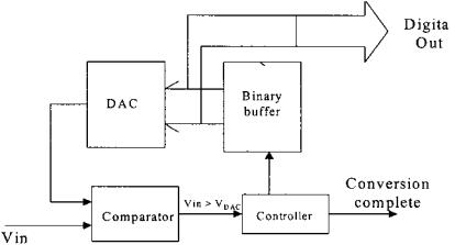
FIGURE 1.13 Block diagram of an analog-to-digital converter. The input analog voltage is compared with the output of a digital-to-analog converter. When the two voltages match, the number held in the binary buffer is equivalent to the input voltage with the resolution of the converter. Different strategies can be used to adjust the contents of the binary buffer to attain a match.
proportional voltage, VDAC. This DAC voltage, VDAC, is then compared to the input voltage, and the binary number in the buffer is adjusted until the desired level of match between VDAC and Vin is obtained. This approach begs the question “How are DAC’s constructed?” In fact, DAC’s are relatively easy to construct using a simple ladder network and the principal of current superposition.
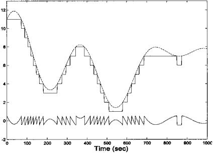
The controller adjusts the binary number based on whether or not the comparator finds the voltage out of the DAC, VDAC, to be greater or less than the input voltage, Vin. One simple adjustment strategy is to increase the binary number by one each cycle if VDAC < Vin, or decrease it otherwise. This so-called tracking ADC is very fast when Vin changes slowly, but can take many cycles when Vin changes abruptly (Figure 1.14). Not only can the conversion time be quite long, but it is variable since it depends on the dynamics of the input signal. This strategy would not easily allow for sampling an analog signal at a fixed rate due to the variability in conversion time.
An alternative strategy termed successive approximation allows the conversion to be done at a fixed rate and is well-suited to digital technology. The successive approximation strategy always takes the same number of cycles irrespective of the input voltage. In the first cycle, the controller sets the most significant bit (MSB) of the buffer to 1; all others are cleared. This binary number is half the maximum possible value (which occurs when all the bits are
Copyright 2004 by Marcel Dekker, Inc. All Rights Reserved.
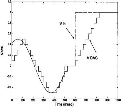
FIGURE 1.14 Voltage waveform of an ADC that uses a tracking strategy. The ADC voltage (solid line) follows the input voltage (dashed line) fairly closely when the input voltage varies slowly, but takes many cycles to “catch up” to an abrupt change in input voltage.
1), so the DAC should output a voltage that is half its maximum voltage—that is, a voltage in the middle of its range. If the comparator tells the controller that Vin > VDAC, then the input voltage, Vin, must be greater than half the maximum range, and the MSB is left set. If Vin < VDAC, then that the input voltage is in the lower half of the range and the MSB is cleared (Figure 1.15). In the next cycle, the next most significant bit is set, and the same comparison is made and the same bit adjustment takes place based on the results of the comparison (Figure 1.15).
After N cycles, where N is the number of bits in the digital output, the voltage from the DAC, VDAC, converges to the best possible fit to the input voltage, Vin. Since Vin VDAC, the number in the buffer, which is proportional to VDAC, is the best representation of the analog input voltage within the resolution of the converter. To signal the end of the conversion process, the ADC puts
Copyright 2004 by Marcel Dekker, Inc. All Rights Reserved.
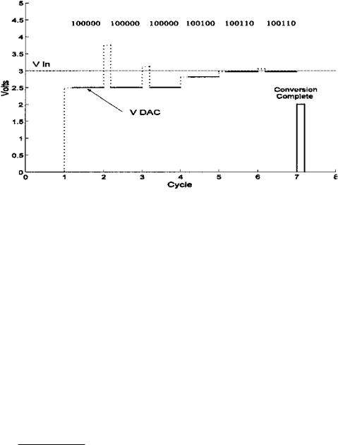
FIGURE 1.15 Vin and VDAC in a 6-bit ADC using the successive approximation strategy. In the first cycle, the MSB is set (solid line) since Vin > VDAC . In the next two cycles, the bit being tested is cleared because Vin < VDAC when this bit was set. For the fourth and fifth cycles the bit being tested remained set and for the last cycle it was cleared. At the end of the sixth cycle a conversion complete flag is set to signify the end of the conversion process.
out a digital signal or flag indicating that the conversion is complete (Figure 1.15).
TIME SAMPLING: BASICS
Time sampling transforms a continuous analog signal into a discrete time signal, a sequence of numbers denoted as x(n) = [x1, x2, x3, . . . xN],* Figure 1.16 (lower trace). Such a representation can be thought of as an array in computer memory. (It can also be viewed as a vector as shown in the next chapter.) Note that the array position indicates a relative position in time, but to relate this number sequence back to an absolute time both the sampling interval and sampling onset time must be known. However, if only the time relative to conversion onset is important, as is frequently the case, then only the sampling interval needs to be
*In many textbooks brackets, [ ], are used to denote digitized variables; i.e., x[n]. Throughout this text we reserve brackets to indicate a series of numbers, or vector, following the MATLAB format.
Copyright 2004 by Marcel Dekker, Inc. All Rights Reserved.

FIGURE 1.16 A continuous signal (upper trace) is sampled at discrete points in time and stored in memory as an array of proportional numbers (lower trace).
known. Converting back to relative time is then achieved by multiplying the sequence number, n, by the sampling interval, Ts: x(t) = x(nTs).
Sampling theory is discussed in the next chapter and states that a sinusoid can be uniquely reconstructed providing it has been sampled by at least two equally spaced points over a cycle. Since Fourier series analysis implies that any signal can be represented is a series of sin waves (see Chapter 3), then by extension, a signal can be uniquely reconstructed providing the sampling frequency is twice that of the highest frequency in the signal. Note that this highest frequency component may come from a noise source and could be well above the frequencies of interest. The inverse of this rule is that any signal that contains frequency components greater than twice the sampling frequency cannot be reconstructed, and, hence, its digital representation is in error. Since this error is introduced by undersampling, it is inherent in the digital representation and no amount of digital signal processing can correct this error. The specific nature of this under-sampling error is termed aliasing and is described in a discussion of the consequences of sampling in Chapter 2.
From a practical standpoint, aliasing must be avoided either by the use of very high sampling rates—rates that are well above the bandwidth of the analog system—or by filtering the analog signal before analog-to-digital conversion. Since extensive sampling rates have an associated cost, both in terms of the
Copyright 2004 by Marcel Dekker, Inc. All Rights Reserved.
ADC required and memory costs, the latter approach is generally preferable. Also note that the sampling frequency must be twice the highest frequency present in the input signal, not to be confused with the bandwidth of the analog signal. All frequencies in the sampled waveform greater than one half the sampling frequency (one-half the sampling frequency is sometimes referred to as the Nyquist frequency) must be essentially zero, not merely attenuated. Recall that the bandwidth is defined as the frequency for which the amplitude is reduced by only 3 db from the nominal value of the signal, while the sampling criterion requires that the value be reduced to zero. Practically, it is sufficient to reduce the signal to be less than quantization noise level or other acceptable noise level. The relationship between the sampling frequency, the order of the anti-aliasing filter, and the system bandwidth is explored in a problem at the end of this chapter.
Example 1.1. An ECG signal of 1 volt peak-to-peak has a bandwidth of 0.01 to 100 Hz. (Note this frequency range has been established by an official standard and is meant to be conservative.) Assume that broadband noise may be present in the signal at about 0.1 volts (i.e., −20 db below the nominal signal level). This signal is filtered using a four-pole lowpass filter. What sampling frequency is required to insure that the error due to aliasing is less than −60 db (0.001 volts)?
Solution. The noise at the sampling frequency must be reduced another 40 db (20 * log (0.1/0.001)) by the four-pole filter. A four-pole filter with a cutoff of 100 Hz (required to meet the fidelity requirements of the ECG signal) would attenuate the waveform at a rate of 80 db per decade. For a four-pole filter the asymptotic attenuation is given as:
Attenuation = 80 log( f2/fc) db
To achieve the required additional 40 db of attenuation required by the problem from a four-pole filter:
80 log( f2/fc) = 40 log( f2/fc) = 40/80 = 0.5 f2/fc = 10.5 =; f2 = 3.16 × 100 = 316 Hz
Thus to meet the sampling criterion, the sampling frequency must be at least 632 Hz, twice the frequency at which the noise is adequately attenuated. The solution is approximate and ignores the fact that the initial attenuation of the filter will be gradual. Figure 1.17 shows the frequency response characteristics of an actual 4-pole analog filter with a cutoff frequency of 100 Hz. This figure shows that the attenuation is 40 db at approximately 320 Hz. Note the high sampling frequency that is required for what is basically a relatively low frequency signal (the ECG). In practice, a filter with a sharper cutoff, perhaps
Copyright 2004 by Marcel Dekker, Inc. All Rights Reserved.
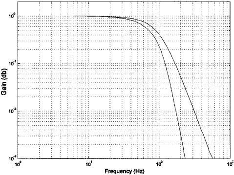
FIGURE 1.17 Detailed frequency plot (on a log-log scale) of a 4-pole and 8-pole filter, both having a cutoff frequency of 100 Hz.
an 8-pole filter, would be a better choice in this situation. Figure 1.17 shows that the frequency response of an 8-pole filter with the same 100 Hz frequency provides the necessary attenuation at less than 200 Hz. Using this filter, the sampling frequency could be lowered to under 400 Hz.
FURTHER STUDY: BUFFERING
AND REAL-TIME DATA PROCESSING
Real-time data processing simply means that the data is processed and results obtained in sufficient time to influence some ongoing process. This influence may come directly from the computer or through human intervention. The processing time constraints naturally depend on the dynamics of the process of interest. Several minutes might be acceptable for an automated drug delivery system, while information on the electrical activity the heart needs to be immediately available.
Copyright 2004 by Marcel Dekker, Inc. All Rights Reserved.
The term buffer, when applied digital technology, usually describes a set of memory locations used to temporarily store incoming data until enough data is acquired for efficient processing. When data is being acquired continuously, a technique called double buffering can be used. Incoming data is alternatively sent to one of two memory arrays, and the one that is not being filled is processed (which may involve simply transfer to disk storage). Most ADC software packages provide a means for determining which element in an array has most recently been filled to facilitate buffering, and frequently the ability to determine which of two arrays (or which half of a single array) is being filled to facilitate double buffering.
DATA BANKS
With the advent of the World Wide Web it is not always necessary to go through the analog-to-digital conversion process to obtain digitized data of physiological signals. A number of data banks exist that provide physiological signals such as ECG, EEG, gait, and other common biosignals in digital form. Given the volatility and growth of the Web and the ease with which searches can be made, no attempt will be made to provide a comprehensive list of appropriate Websites. However, a good source of several common biosignals, particularly the ECG, is the Physio Net Data Bank maintained by MIT—http://www.physionet.org. Some data banks are specific to a given set of biosignals or a given signal processing approach. An example of the latter is the ICALAB Data Bank in Japan—http:// www.bsp.brain.riken.go.jp/ICALAB/—which includes data that can be used to evaluate independent component analysis (see Chapter 9) algorithms.
Numerous other data banks containing biosignals and/or images can be found through a quick search of the Web, and many more are likely to come online in the coming years. This is also true for some of the signal processing algorithms as will be described in more detail later. For example, the ICALAB Website mentioned above also has algorithms for independent component analysis in MATLAB m-file format. A quick Web search can provide both signal processing algorithms and data that can be used to evaluate a signal processing system under development. The Web is becoming an evermore useful tool in signal and image processing, and a brief search of the Web can save considerable time in the development process, particularly if the signal processing system involves advanced approaches.
PROBLEMS
1. A single sinusoidal signal is contained in noise. The RMS value of the noise is 0.5 volts and the SNR is 10 db. What is the peak-to-peak amplitude of the sinusoid?
Copyright 2004 by Marcel Dekker, Inc. All Rights Reserved.
2.A resistor produces 10 µV noise when the room temperature is 310°K and the bandwidth is 1 kHz. What current noise would be produced by this resistor?
3.The noise voltage out of a 1 MΩ resistor was measured using a digital volt meter as 1.5 µV at a room temperature of 310 °K. What is the effective bandwidth of the voltmeter?
4.The photodetector shown in Figure 1.4 has a sensitivity of 0.3µA/µW (at a
wavelength of 700 nm). In this circuit, there are three sources of noise. The photodetector has a dark current of 0.3 nA, the resistor is 10 MΩ, and the amplifier has an input current noise of 0.01 pA/√Hz. Assume a bandwidth of
10kHz. (a) Find the total noise current input to the amplifier. (b) Find the minimum light flux signal that can be detected with an SNR = 5.
5.A lowpass filter is desired with the cutoff frequency of 10 Hz. This filter should attenuate a 100 Hz signal by a factor of 85. What should be the order of this filter?
6.You are given a box that is said to contain a highpass filter. You input a series of sine waves into the box and record the following output:
Frequency (Hz): |
2 |
10 |
20 |
60 |
100 |
125 |
150 |
200 |
300 |
400 |
Vout volts rms: |
.15×10−7 |
0.1×10⁻³ |
0.002 |
0.2 |
1.5 |
3.28 |
4.47 |
4.97 |
4.99 |
5.0 |
What is the cutoff frequency and order of this filter?
7.An 8-bit ADC converter that has an input range of ± 5 volts is used to convert a signal that varies between ± 2 volts. What is the SNR of the input if the input noise equals the quantization noise of the converter?
8.As elaborated in Chapter 2, time sampling requires that the maximum frequency present in the input be less than fs/2 for proper representation in digital format. Assume that the signal must be attenuated by a factor of 1000 to be considered “not present.” If the sampling frequency is 10 kHz and a 4th-order lowpass anti-aliasing filter is used prior to analog-to-digital conversion, what should be the bandwidth of the sampled signal? That is, what must the cutoff frequency be of the anti-aliasing lowpass filter?
Copyright 2004 by Marcel Dekker, Inc. All Rights Reserved.