

3.6 SYSTEM CONTROL
The system control inputs are used to reset the processor, to halt the processor, and to signal a bus error to the processor. The outputs reset the external devices in the system and signal a processor error halt to those devices. The three system control signals are described in the following paragraphs.
Bus Error ( |
) |
This input signal indicates a problem in the current bus cycle. The problem may be the following:
1.No response from a device.
2.No interrupt vector number returned.
3.An illegal access request rejected by a memory management unit.
4.Some other application-dependent error.
Either the processor retries the bus cycle or performs exception processing, as determined by interaction between the bus error signal and the halt signal.
Reset ( )
The external assertion of this bidirectional signal along with the assertion of HALT starts a system initialization sequence by resetting the processor. The processor assertion of RESET (from executing a RESET instruction) resets all external devices of a system without affecting the internal state of the processor. To reset both the processor and the external devices, the RESET and HALT input signals must be asserted at the same time.
Halt ( )
An input to this bidirectional signal causes the processor to stop bus activity at the completion of the current bus cycle. This operation places all control signals in the inactive state and places all three-state lines in the high-impedance state (refer to Table 3-4).
When the processor has stopped executing instructions (in the case of a double bus fault condition, for example), the HALT line is driven by the processor to indicate the condition to external devices.
Mode (MODE) (MC68HC001/68EC000)
The MODE input selects between the 8-bit and 16-bit operating modes. If this input is grounded at reset, the processor will come out of reset in the 8-bit mode. If this input is tied high or floating at reset, the processor will come out of reset in the 16-bit mode. This input should be changed only at reset and must be stable two clocks after RESET is negated. Changing this input during normal operation may produce unpredictable results.
MOTOROLA |
M68000 8-/16-/32-BIT MICROPROCESSORS USER'S MANUAL |
3-7 |
3.7 M6800 PERIPHERAL CONTROL
These control signals are used to interface the asynchronous M68000 processors with the synchronous M6800 peripheral devices. These signals are described in the following paragraphs.
Enable (E)
This signal is the standard enable signal common to all M6800 Family peripheral devices. A single period of clock E consists of 10 MC68000 clock periods (six clocks low, four clocks high). This signal is generated by an internal ring counter that may come up in any state. (At power-on, it is impossible to guarantee phase relationship of E to CLK.) The E signal is a free-running clock that runs regardless of the state of the MPU bus.
Valid Peripheral Address ( |
) |
This input signal indicates that the device or memory area addressed is an M6800
Family device or a memory area assigned to M6800 Family devices and that data transfer should be synchronized with the E signal. This input also indicates that the processor should use automatic vectoring for an interrupt. Refer to Appendix B M6800 Peripheral Interface.
Valid Memory Address ( |
) |
This output signal indicates to M6800 peripheral devices that the address on the address bus is valid and that the processor is synchronized to the E signal. This signal only responds to a VPA input that identifies an M6800 Family device.
The MC68008 does not supply a VMA signal. This signal can be produced by a transistor-to-transistor logic (TTL) circuit; an example is described in Appendix B M6800 Peripheral Interface.
3.8 PROCESSOR FUNCTION CODES (FC0, FC1, FC2)
These function code outputs indicate the mode (user or supervisor) and the address space type currently being accessed, as shown in Table 3-3. The function code outputs are valid whenever AS is active.
3-8 |
M68000 8-/16-/32-BIT MICROPROCESSORS USER'S MANUAL |
MOTOROLA |
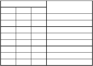
Table 3-3. Function Code Outputs
Function Code Output |
|
||
FC2 |
FC1 |
FC0 |
Address Space Type |
Low |
Low |
Low |
(Undefined, Reserved) |
Low |
Low |
High |
User Data |
Low |
High |
Low |
User Program |
Low |
High |
High |
(Undefined, Reserved) |
High |
Low |
Low |
(Undefined, Reserved) |
High |
Low |
High |
Supervisor Data |
High |
High |
Low |
Supervisor Program |
High |
High |
High |
CPU Space |
3.9 CLOCK (CLK)
The clock input is a TTL-compatible signal that is internally buffered for development of the internal clocks needed by the processor. This clock signal is a constant frequency square wave that requires no stretching or shaping. The clock input should not be gated off at any time, and the clock signal must conform to minimum and maximum pulse-width times listed in Section 10 Electrical Characteristics.
3.10 POWER SUPPLY (VCC and GND)
Power is supplied to the processor using these connections. The positive output of the power supply is connected to the VCC pins and ground is connected to the GND pins.
MOTOROLA |
M68000 8-/16-/32-BIT MICROPROCESSORS USER'S MANUAL |
3-9 |
3.11 SIGNAL SUMMARY
Table 3-4 summarizes the signals discussed in the preceding paragraphs.
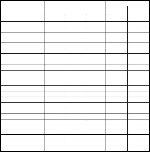
Table 3-4. Signal Summary
|
|
|
|
|
Hi-Z |
Signal Name |
Mnemonic |
Input/Output |
Active State |
On |
On Bus |
|
|
|
|
|
Relinquish |
Address Bus |
A0–A23 |
Output |
High |
Yes |
Yes |
Data Bus |
D0–D15 |
Input/Output |
High |
Yes |
Yes |
Address Strobe |
AS |
Output |
Low |
No |
Yes |
Read/Write |
R/W |
Output |
Read-High |
No |
Yes |
|
|
|
Write-Low |
|
|
Data Strobe |
DS |
Output |
Low |
No |
Yes |
Upper and Lower Data Strobes |
UDS, LDS |
Output |
Low |
No |
Yes |
Data Transfer Acknowledge |
DTACK |
Input |
Low |
No |
No |
Bus Request |
BR |
Input |
Low |
No |
No |
Bus Grant |
BG |
Output |
Low |
No |
No |
Bus Grant Acknowledge |
BGACK |
Input |
Low |
No |
No |
Interrupt Priority Level |
IPL0, IPL1, |
Input |
Low |
No |
No |
|
IPL2 |
|
|
|
|
Bus Error |
BERR |
Input |
Low |
No |
No |
Mode |
MODE |
Input |
High |
— |
— |
Reset |
RESET |
Input/Output |
Low |
No* |
No* |
Halt |
HALT |
Input/Output |
Low |
No* |
No* |
Enable |
E |
Output |
High |
No |
No |
Valid Memory Address |
VMA |
Output |
Low |
No |
Yes |
Valid Peripheral Address |
VPA |
Input |
Low |
No |
No |
Function Code Output |
FC0, FC1, |
Output |
High |
No |
Yes |
|
FC2 |
|
|
|
|
Clock |
CLK |
Input |
High |
No |
No |
Power Input |
VCC |
Input |
— |
— |
— |
Ground |
GND |
Input |
— |
— |
— |
*Open drain. |
|
|
|
|
|
3-10 |
M68000 8-/16-/32-BIT MICROPROCESSORS USER'S MANUAL |
MOTOROLA |