

is lost through the active P-channel transistor. Also, since only one transistor is turned on during the steady state, power consumption is determined by leakage currents.
Because the basic CMOS cell is composed of two complementary transistors, a virtual semiconductor controlled rectifier (SCR) may be formed when an input exceeds the supply voltage. The SCR that is formed by this high input causes the device to become latched in a mode that may result in excessive current drain and eventual destruction of the device. Although the MC68HC000 and MC68EC000 is implemented with input protection diodes, care should be exercised to ensure that the maximum input voltage specification is not exceeded. Some systems may require that the CMOS circuitry be isolated from voltage transients; other may require additional circuitry.
The MC68HC000 and MC68EC000, implemented in CMOS, is applicable to designs to which the following considerations are relevant:
1.The MC68HC000 and MC68EC000 completely satisfies the input/output drive requirements of CMOS logic devices.
2.The HCMOS MC68HC000 and MC68EC000 provides an order of magnitude reduction in power dissipation when compared to the HMOS MC68000. However, the MC68HC000 does not offer a "power-down" mode.
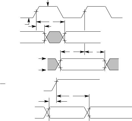
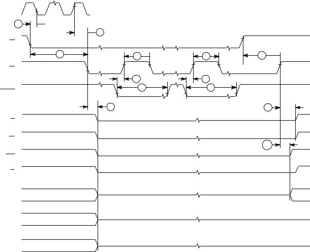
10.5 AC ELECTRICAL SPECIFICATION DEFINITIONS
The AC specifications presented consist of output delays, input setup and hold times, and signal skew times. All signals are specified relative to an appropriate edge of the clock and possibly to one or more other signals.
The measurement of the AC specifications is defined by the waveforms shown in Figure 10-2. To test the parameters guaranteed by Motorola, inputs must be driven to the voltage levels specified in the figure. Outputs are specified with minimum and/or maximum limits, as appropriate, and are measured as shown. Inputs are specified with minimum setup and hold times, and are measured as shown. Finally, the measurement for signal-to-signal specifications are shown.
NOTE
The testing levels used to verify conformance to the AC specifications does not affect the guaranteed DC operation of the device as specified in the DC electrical characteristics.
MOTOROLA |
M68000 8-/16-/32-BIT MICROPROCESSORS USER'S MANUAL |
10-5 |
|
|
|
DRIVE |
|
|
|
|
|
|
TO 2.4 V |
|
|
|
BCLK |
1.5 V |
|
1.5 V |
|
||
|
DRIVE TO |
|
A |
|
|
|
|
0.5 V |
B |
|
|
|
|
|
|
|
|
|
||
|
VALID |
2.0 V |
2.0 |
VALID |
|
|
OUTPUTS(1) |
n |
V |
n + 1 |
|||
OUTPUT |
OUTPUT |
|||||
|
0.8 V |
|||||
|
|
0.8 V |
|
|
||
|
|
|
C |
|
D |
|
|
DRIVE TO |
2.0 V |
|
2.0 V |
||
INPUTS(2) |
|
2.4 V |
VALID |
|||
|
|
|
|
|||
|
|
|
INPUT |
|
||
|
DRIVE TO |
0.8 V |
0.8 V |
|||
|
|
|||||
|
|
0.5 V |
|
|
|
|
2.0 V
RSTI (3)
F
E
2.0 V
0.8 V
NOTES:
1.This output timing is applicable to all parameters specified relative to the rising edge of the clock.
2.This input timing is applicable to all parameters specified relative to the rising edge of the clock.
3.This timing is applicable to all parameters specified relative to the negation of the RESET signal.
LEGEND:
A.Maximum output delay specification.
B.Minimum output hold time.
C.Minimum input setup time specification.
D.Minimum input hold time specification.
E.Mode select setup time to RESET negated.
F.Mode select hold time from RESET negated.
Figure 10-2. Drive Levels and Test Points for AC Specifications
10-6 |
M68000 8-/16-/32-BIT MICROPROCESSORS USER'S MANUAL |
MOTOROLA |

10.6 MC68000/68008/68010 DC ELECTRICAL CHARACTERISTICS
(VCC=5.0 VDC±5%; GND=0 VDC; TA=TL TO TH)
|
Characteristic |
|
Input High Voltage |
|
|
Input Low Voltage |
|
|
Input Leakage Current |
BERR, BGACK, BR, DTACK, CLK, IPL0—IPL2, VPA |
|
@ 5.25 V |
|
HALT, RESET |
Three-State (Off State) Input Current |
AS, A1—A23, D0—D15, FC0—FC2, |
|
@ 2.4 V/0.4 V |
|
LDS, R/ W, UDS, VMA |
Output High Voltage (IOH = –400 µA) |
E* |
|
(I OH = -400 µA) |
|
AS, A1–A23, BG, D0–D15, |
|
|
FC0–FC2, LDS, R/ W, UDS, VMA |
Output Low Voltage |
|
|
(IOL= 1.6 mA) |
|
HALT |
(IOL = 3.2 mA) |
|
A1—A23, BG, FC0-FC2 |
(IOL = 5.0 mA) |
|
RESET |
(IOL = 5.3 mA) |
|
E, AS, D0—D15, LDS, R/ W, UDS, VMA |
Power Dissipation (see POWER CONSIDERATIONS) |
||
Capacitance (Vin=0 V, TA=25°C, Frequency=1 MHz)** |
||
Load Capacitance |
|
HALT |
|
|
All Others |
Symbol |
Min |
Max |
Unit |
VIH |
2.0 |
VCC |
V |
VIL |
GND-0.3 |
0.8 |
V |
IIN |
— |
2.5 |
µA |
—20
ITSI |
— |
20 |
µA |
VOH |
VCC –0.75 |
— |
V |
|
2.4 |
2.4 |
|
VOL |
— |
0.5 |
V |
|
|
||
|
— |
0.5 |
|
|
— |
0.5 |
|
|
— |
0.5 |
|
PD*** |
— |
— |
W |
Cin |
— |
20.0 |
pF |
CL |
— |
70 |
pF |
|
— |
130 |
|
*With external pullup resistor of 1.1 Ω.
**Capacitance is periodically sampled rather than 100% tested.
***During normal operation, instantaneous VCC current requirements may be as high as 1.5 A.
MOTOROLA |
M68000 8-/16-/32-BIT MICROPROCESSORS USER'S MANUAL |
10-7 |
10.7 DC ELECTRICAL CHARACTERISTICS (VCC =5.0 VDC±5%; GND=0 VDC; TA=TL
TO TH) (Applies To All Processors Except The MC68EC000)
|
Characteristic |
|
Input High Voltage |
|
|
Input Low Voltage |
|
|
Input Leakage Current |
BERR, BGACK, BR, DTACK, CLK, IPL0—IPL2, VPA |
|
@ 5.25 V |
|
MODE, HALT, RESET |
Three-State (Off State) Input Current |
AS, A0—A23, D0—D15, |
|
@ 2.4 V/0.4 V |
|
FC0–FC2, LDS, R/ W, UDS, VMA |
Output High Voltage |
|
E, AS, A0–A23, BG, D0–D15, |
|
|
FC0–FC2, LDS, R/ W, UDS, VMA |
Output Low Voltage |
|
|
(IOL = 1.6 mA) |
|
HALT |
(IOL = 3.2 mA) |
|
A0—A23, BG, FC0-FC2 |
(IOL = 5.0 mA) |
|
RESET |
(IOL = 5.3 mA) |
|
E, AS, D0—D15, LDS, R/ W, UDS, VMA |
Current Dissipation* |
|
f = 8 MHz |
|
|
f = 10 MHz |
|
|
f = 12.5 MHz |
|
|
f = 16.67 MHz |
|
|
f = 20 MHz |
Power Dissipation |
|
f = 8 MHz |
|
|
f = 10 MHz |
|
|
f = 12.5 MHz |
|
|
f = 16.67 MHz |
|
|
f = 20 MHz |
Capacitance (Vin = 0 V, T A=25°C, Frequency=1 MHz)** |
||
Load Capacitance |
|
HALT |
|
|
All Others |
Symbol |
Min |
Max |
Unit |
VIH |
2.0 |
VCC |
V |
VIL |
GND-0.3 |
0.8 |
V |
IIN |
— |
2.5 |
A |
—20
ITSI |
— |
20 |
A |
VOH |
VCC –0.75 |
— |
V |
VOL |
— |
0.5 |
V |
|
|
||
|
— |
0.5 |
|
|
— |
0.5 |
|
|
— |
0.5 |
|
ID |
— |
25 |
mA |
|
— |
30 |
|
|
— |
35 |
|
|
— |
50 |
|
|
— |
70 |
|
PD |
— |
0.13 |
W |
|
|
0.16 |
|
|
|
0.19 |
|
|
|
0.26 |
|
|
|
0.38 |
|
Cin |
— |
20.0 |
pF |
CL |
— |
70 |
pF |
|
— |
130 |
|
*Current listed are with no loading.
**Capacitance is periodically sampled rather than 100% tested.
10.8 AC ELECTRICAL SPECIFICATIONS — CLOCK TIMING (See Figure 10-3)
(Applies To All Processors Except The MC68EC000)
Num |
Characteristic |
8 MHz* |
10 MHz* |
12.5 MHz* |
16.67 MHz |
16 MHz |
20 MHZ ** |
Unit |
|||||||
12F |
|||||||||||||||
|
|
|
|
|
|
|
|
|
|
|
|
|
|||
|
|
Min |
Max Min Max Min Max |
Min |
Max |
Min |
Max |
Min |
Max |
|
|||||
|
Frequency of Operation |
4.0 |
8.0 |
4.0 |
10.0 |
4.0 |
12.5 |
8.0 |
16.7 |
8.0 |
16.7 |
8.0 |
20.0 |
MHz |
|
1 |
Cycle Time |
125 |
250 |
100 |
250 |
80 |
250 |
60 |
125 |
60 |
125 |
50 |
125 |
ns |
|
2,3 |
Clock Pulse Width |
55 |
125 |
45 |
125 |
35 |
125 |
27 |
62.5 |
27 |
62.5 |
21 |
62.5 |
ns |
|
|
(Measured from 1.5 V to 1.5 |
55 |
125 |
45 |
125 |
35 |
125 |
27 |
62.5 |
27 |
62.5 |
21 |
62.5 |
|
|
|
V for 12F) |
|
|
|
|
|
|
|
|
|
|
|
|
|
|
4,5 |
Clock Rise and Fall Times |
— |
10 |
— |
10 |
— |
5 |
— |
5 |
— |
5 |
— |
4 |
ns |
|
|
|
— |
10 |
— |
10 |
— |
5 |
— |
5 |
— |
5 |
— |
4 |
|
|
*These specifications represent an improvement over previously published specifications for the 8-, 10-, and 12.5- MHz MC68000 and are valid only for product bearing date codes of 8827 and later.
**This frequency applies only to MC68HC000 and MC68EC000 parts.
10-8 |
M68000 8-/16-/32-BIT MICROPROCESSORS USER'S MANUAL |
MOTOROLA |
10.9 MC68008 AC ELECTRICAL SPECIFICATIONS — CLOCK TIMING (See
Figure 10-3)
Num |
Characteristic |
8 MHz* |
10 MHz* |
Unit |
||
|
|
Min |
Max |
Min |
Max |
|
|
Frequency of Operation |
2.0 |
8.0 |
2.0 |
10.0 |
MHz |
1 |
Cycle Time |
125 |
500 |
100 |
500 |
ns |
2,3 |
Clock Pulse Width |
55 |
250 |
45 |
250 |
ns |
4,5 |
Clock Rise and Fall Times |
— |
10 |
— |
10 |
ns |
*These specifications represent an improvement over previously published specifications for the 8-, and 10-MHz MC68008 and are valid only for product bearing date codes of 8827 and later
1
2 
 3
3 
2.0V
0.8V
4 |
5 |
NOTE: Timing measurements are referenced to and from a low voltage of 0.8 V and a high voltage of 2.0 V, unless otherwise noted. The voltage swing through this range should start outside and pass through the range such that the rise or fall will be linear between. 0.8 V and 2.0 V.
Figure 10-3. Clock Input Timing Diagram
MOTOROLA |
M68000 8-/16-/32-BIT MICROPROCESSORS USER'S MANUAL |
10-9 |
10.10 AC ELECTRICAL SPECIFICATIONS — READ AND WRITE CYCLES
(VCC=5.0 VDC±5+; GND=0 V; TA=TL to TH; (see Figures 10-4 and 10-5) (Applies To All Processors Except The MC68EC000)
Num |
Characteristic |
8 MHz* |
10 MHz* |
12.5 MHz* |
16.67 MHz |
16 MHz |
20 MHz •• |
Unit |
|||||||
|
12F |
|
|||||||||||||
|
|
|
|
|
|
|
|
|
|
|
|
|
|
|
|
|
|
Min |
Max |
Min |
Max |
Min |
Max Min Max |
Min |
Max |
Min |
Max |
|
|||
6 |
Clock Low to Address Valid |
— |
62 |
— |
50 |
— |
50 |
— |
50 |
|
30 |
— |
25 |
ns |
|
6A |
Clock High to FC Valid |
— |
62 |
— |
50 |
— |
45 |
— |
45 |
0 |
30 |
0 |
25 |
ns |
|
7 |
Clock High to Address, Data |
— |
80 |
— |
70 |
— |
60 |
— |
50 |
|
50 |
— |
42 |
ns |
|
|
Bus High Impedance |
|
|
|
|
|
|
|
|
|
|
|
|
|
|
|
(Maximum) |
|
|
|
|
|
|
|
|
|
|
|
|
|
|
8 |
Clock High to Address, FC |
0 |
— |
0 |
— |
0 |
— |
0 |
— |
0 |
— |
0 |
— |
ns |
|
|
Invalid (Minimum) |
|
|
|
|
|
|
|
|
|
|
|
|
|
|
91 |
Clock High to AS, DS |
3 |
60 |
3 |
50 |
3 |
40 |
3 |
|
40 |
3 |
30 |
3 |
25 |
ns |
|
Asserted |
|
|
|
|
|
|
|
|
|
|
|
|
|
|
112 |
Address Valid to AS, DS |
30 |
— |
20 |
— |
15 |
— |
15 |
— |
15 |
— |
10 |
— |
ns |
|
|
Asserted (Read)/AS Asserted |
|
|
|
|
|
|
|
|
|
|
|
|
|
|
|
(Write) |
|
|
|
|
|
|
|
|
|
|
|
|
|
|
11A2 |
FC Valid to AS), DS Asserted |
90 |
— |
70 |
— |
60 |
— |
30 |
— |
45 |
— |
40 |
— |
ns |
|
|
(Read)/AS) Asserted (Write) |
|
|
|
|
|
|
|
|
|
|
|
|
|
|
121 |
Clock Low to AS, DS Negated |
— |
62 |
— |
50 |
— |
40 |
— |
40 |
3 |
30 |
3 |
25 |
ns |
|
132 |
AS, DS Negated to Address, |
40 |
— |
30 |
— |
20 |
— |
10 |
— |
15 |
— |
10 |
— |
ns |
|
|
FC Invalid |
|
|
|
|
|
|
|
|
|
|
|
|
|
|
142 |
ASand DS Read) Width |
270 |
— |
195 |
— |
160 |
— |
120 |
— |
120 |
— |
100 |
— |
ns |
|
|
Asserted |
|
|
|
|
|
|
|
|
|
|
|
|
|
|
14A |
DS Width Asserted (Write) |
140 |
|
95 |
|
80 |
|
60 |
|
60 |
— |
50 |
— |
ns |
|
152 |
AS, DS Width Negated |
150 |
— |
105 |
— |
65 |
— |
60 |
— |
60 |
— |
50 |
— |
ns |
|
16 |
Clock High to Control Bus |
— |
80 |
— |
70 |
— |
60 |
— |
50 |
— |
50 |
— |
42 |
ns |
|
|
High Impedance |
|
|
|
|
|
|
|
|
|
|
|
|
|
|
172 |
AS, DS Negated to R/W |
40 |
— |
30 |
— |
20 |
— |
10 |
— |
15 |
— |
10 |
— |
ns |
|
|
Invalid |
|
|
|
|
|
|
|
|
|
|
|
|
|
|
181 |
Clock High to R/W High |
0 |
55 |
0 |
45 |
0 |
40 |
0 |
|
40 |
0 |
30 |
0 |
25 |
ns |
|
(Read) |
|
|
|
|
|
|
|
|
|
|
|
|
|
|
201 |
Clock High to R/W Low |
0 |
55 |
0 |
45 |
0 |
40 |
0 |
|
40 |
0 |
30 |
0 |
25 |
ns |
|
(Write) |
|
|
|
|
|
|
|
|
|
|
|
|
|
|
20A2,6 |
AS Asserted to R/W Valid |
— |
10 |
— |
10 |
— |
10 |
— |
10 |
— |
10 |
— |
10 |
ns |
|
|
(Write) |
|
|
|
|
|
|
|
|
|
|
|
|
|
|
212 |
Address Valid to R/W Low |
20 |
— |
0 |
— |
0 |
— |
0 |
— |
0 |
— |
0 |
— |
ns |
|
|
(Write) |
|
|
|
|
|
|
|
|
|
|
|
|
|
|
21A2 |
FC Valid to R/W Low (Write) |
60 |
— |
50 |
— |
30 |
— |
20 |
— |
30 |
— |
25 |
— |
ns |
|
222 |
R/ W Low to DS Asserted |
80 |
— |
50 |
— |
30 |
— |
20 |
— |
30 |
— |
25 |
— |
ns |
|
|
(Write) |
|
|
|
|
|
|
|
|
|
|
|
|
|
|
23 |
Clock Low to Data-Out Valid |
— |
62 |
— |
50 |
— |
50 |
— |
550 |
— |
30 |
— |
25 |
ns |
|
|
(Write) |
|
|
|
|
|
|
|
|
|
|
|
|
|
|
252 |
AS, DS) Negated to Data-Out |
401 |
— |
30 |
— |
20 |
— |
15 |
— |
15 |
— |
10 |
— |
ns |
|
|
Invalid (Write) |
0 |
|
|
|
|
|
|
|
|
|
|
|
|
|
10-10 |
M68000 8-/16-/32-BIT MICROPROCESSORS USER'S MANUAL |
MOTOROLA |
Num |
Characteristic |
8 MHz* |
10 MHz* |
12.5 MHz* |
16.67 MHz |
16 MHz |
20 MHz •• |
Unit |
||||||||
|
12F |
|||||||||||||||
|
|
|
|
|
|
|
|
|
|
|
|
|
|
|
||
|
|
Min |
Max |
Min |
Max |
Min Max |
Min Max |
Min |
Max |
Min |
|
Max |
|
|||
262 |
Data-Out Valid to DS Asserted |
40 |
— |
30 |
— |
20 |
— |
15 |
— |
15 |
— |
10 |
— |
|
ns |
|
|
(Write) |
|
|
|
|
|
|
|
|
|
|
|
|
|
|
|
275 |
Data-In Valid to Clock Low |
10 |
— |
10 |
— |
10 |
— |
7 |
— |
5 |
— |
5 |
— |
|
ns |
|
|
(Setup Time on Read) |
|
|
|
|
|
|
|
|
|
|
|
|
|
|
|
27A5 |
Late BERR Asserted to Clock |
45 |
— |
45 |
— |
45 |
— |
— |
— |
— |
— |
— |
— |
ns |
|
|
|
Low (setup Time) |
|
|
|
|
|
|
|
|
|
|
|
|
|
|
|
282 |
AS, DS Negated to DTACK |
0 |
2401 |
0 |
190 |
0 |
150 |
0 |
110 |
0 |
110 |
0 |
|
95 |
ns |
|
|
Negated (Asynchronous Hold) |
|
1 |
|
|
|
|
|
|
|
|
|
|
|
|
|
28A |
AS, DS Negated to Data-In |
— |
187 |
— |
150 |
— |
120 |
— 110 |
— |
110 |
— |
95 |
|
ns |
|
|
|
High Impedance |
|
|
|
|
|
|
|
|
|
|
|
|
|
|
|
29 |
AS, DS Negated to Data-In |
0 |
— |
0 |
— |
0 |
— |
0 |
— |
0 |
— |
0 |
— |
|
ns |
|
|
Invalid (Hold Time on Read) |
|
|
|
|
|
|
|
|
|
|
|
|
|
|
|
29A |
AS, DS Negated to Data-In |
— |
187 |
— |
150 |
— |
120 |
— |
90 |
— |
90 |
— |
75 |
|
ns |
|
|
High Impedance |
|
|
|
|
|
|
|
|
|
|
|
|
|
|
|
30 |
AS, DS) Negated to BERR |
0 |
— |
0 |
— |
0 |
— |
0 |
— |
0 |
— |
0 |
— |
|
ns |
|
|
Negated |
|
|
|
|
|
|
|
|
|
|
|
|
|
|
|
312,5 |
DTACK Asserted to Data-In |
— |
90 |
— |
65 |
— |
50 |
— |
40 |
— |
50 |
— |
42 |
|
ns |
|
|
Valid (Setup Time) |
|
|
|
|
|
|
|
|
|
|
|
|
|
|
|
32 |
HALT) and RESET Input |
0 |
200 |
0 |
200 |
0 |
200 |
0 |
150 |
— 150 |
0 |
150 |
ns |
|||
|
Transition Time |
|
|
|
|
|
|
|
|
|
|
|
|
|
|
|
33 |
Clock High to BG Asserted |
— |
62 |
— |
50 |
— |
40 |
— |
40 |
0 |
30 |
0 |
25 |
ns |
|
|
34 |
Clock High to BG Negated |
— |
62 |
— |
50 |
— |
40 |
— |
40 |
0 |
30 |
0 |
25 |
ns |
|
|
35 |
BR Asserted to BG Asserted |
1.5 |
3.5 |
1.5 |
3.5 |
1.5 |
3.5 |
1.5 |
|
3.5 |
1.5 |
3.5 |
1.5 |
|
3.5 |
Clks |
367 |
BR Negated toBG Negated |
1.5 |
3.5 |
1.5 |
3.5 |
1.5 |
3.5 |
1.5 |
|
3.5 |
1.5 |
3.5 |
1.5 |
|
3.5 |
Clks |
37 |
BGACK Asserted to BG |
1.5 |
3.5 |
1.5 |
3.5 |
1.5 |
3.5 |
1.5 |
|
3.5 |
1.5 |
3.5 |
1.5 |
|
3.5 |
Clks |
|
Negated |
|
|
|
|
|
|
|
|
|
|
|
|
|
|
|
37A8 |
BGACK Asserted to BR |
20 |
1.5 |
20 |
1.5 |
20 |
1.5 |
10 |
|
1.5 |
10 |
1.5 |
10 |
|
1.5 |
ns |
|
Negated |
|
Clks |
|
Clks |
|
Clks |
|
Clks |
|
Clks |
|
|
Clks |
|
|
38 |
BG Asserted to Control, |
— |
80 |
— |
70 |
— |
60 |
— |
50 |
— |
50 |
— |
42 |
|
ns |
|
|
Address, Data Bus High |
|
|
|
|
|
|
|
|
|
|
|
|
|
|
|
|
Impedance (AS Negated) |
|
|
|
|
|
|
|
|
|
|
|
|
|
|
|
39 |
BG Width Negated |
1.5 |
— |
1.5 |
— |
1.5 |
— |
1.5 |
— |
1.5 |
— |
1.5 |
— |
|
|
clks |
40 |
Clock Low to VMA Asserted |
— |
70 |
— |
70 |
— |
70 |
— |
50 |
— |
50 |
— |
40 |
|
ns |
|
41 |
Clock Low to E Transition |
— |
55 12 |
— |
45 |
— |
35 |
— |
35 |
— |
35 |
— |
30 |
|
ns |
|
42 |
E Output Rise and Fall Time |
— |
15 |
— |
15 |
— |
15 |
— |
15 |
— |
15 |
— |
12 |
|
ns |
|
43 |
VMA Asserted to E High |
200 |
— |
150 |
— |
90 |
— |
80 |
— |
80 |
— |
60 |
— |
|
ns |
|
44 |
AS, DS Negated to VPA |
0 |
120 |
0 |
90 |
0 |
70 |
0 |
|
50 |
0 |
50 |
0 |
|
42 |
ns |
|
Negated |
|
|
|
|
|
|
|
|
|
|
|
|
|
|
|
45 |
E Low to Control, Address |
30 |
— |
10 |
— |
10 |
— |
10 |
— |
10 |
— |
10 |
— |
|
ns |
|
|
Bus Invalid (Address Hold |
|
|
|
|
|
|
|
|
|
|
|
|
|
|
|
|
Time) |
|
|
|
|
|
|
|
|
|
|
|
|
|
|
|
46 |
BGACK Width Low |
1.5 |
— |
1.5 |
— |
1.5 |
— |
1.5 |
— |
1.5 |
— |
1.5 |
— |
|
ns |
|
MOTOROLA |
M68000 8-/16-/32-BIT MICROPROCESSORS USER'S MANUAL |
10-11 |
Num |
Characteristic |
8 MHz* |
10 MHz* |
12.5 MHz* |
16.67 MHz |
16 MHz |
20 MHz •• |
Unit |
|||||||
|
12F |
||||||||||||||
|
|
|
|
|
|
|
|
|
|
|
|
|
|
||
|
|
Min |
Max |
Min |
Max |
Min |
Max Min |
Max |
Min |
Max |
Min |
Max |
|
||
475 |
Asynchronous Input Setup |
10 |
— |
10 |
— |
10 |
— |
10 |
— |
5 |
— |
5 |
— |
ns |
|
|
Time |
|
|
|
|
|
|
|
|
|
|
|
|
|
|
482, 3 |
BERR Asserted to DTACK |
20 |
— |
20 |
— |
20 |
— |
10 |
— |
10 |
— |
10 |
— |
ns |
|
|
Asserted |
|
|
|
|
|
|
|
|
|
|
|
|
|
|
482,3,5 |
DTACK Asserted to BERR |
— |
80 |
— |
55 |
— |
35 |
— |
— |
— |
— |
— |
— |
ns |
|
|
Asserted (MC68010 Only) |
|
|
|
|
|
|
|
|
|
|
|
|
|
|
499 |
AS, DS, Negated to E Low |
-70 |
70 |
-55 |
55 |
-45 |
45 |
-35 |
35 |
-35 |
35 |
–30 |
30 |
ns |
|
50 |
E Width High |
450 |
— |
350 — 280 — 220 — 220 |
— |
190 |
— |
ns |
|
||||||
51 |
E Width Low |
700 |
— |
550 |
— |
440 |
— |
340 |
— |
340 |
— |
290 |
— |
ns |
|
53 |
Data-Out Hold from Clock |
0 |
— |
0 |
— |
0 |
— |
0 |
— |
0 |
— |
0 |
— |
ns |
|
|
High |
|
|
|
|
|
|
|
|
|
|
|
|
|
|
54 |
E Low to Data-Out Invalid |
30 |
— |
20 |
— |
15 |
— |
10 |
— |
10 |
— |
5 |
— |
ns |
|
55 |
R/ W Asserted to Data Bus |
30 |
— |
20 |
— |
10 |
— |
0 |
— |
0 |
— |
0 |
— |
ns |
|
|
Impedance Change |
|
|
|
|
|
|
|
|
|
|
|
|
|
|
564 |
HALT ( RESETPulse Width |
10 |
— |
10 |
— |
10 |
— |
10 |
— |
10 |
— |
10 |
— |
|
clks |
57 |
BGACK Negated to AS, DS, |
1.5 |
— |
1.5 |
— |
1.5 |
— |
1.5 |
— |
1.5 |
— |
1.5 |
— |
clks |
|
|
R/ W Driven |
|
|
|
|
|
|
|
|
|
|
|
|
|
|
57A |
BGACK Negated to FC, VMA |
1 |
— |
1 |
— |
1 |
— |
1 |
— |
1 |
— |
1 |
— |
clks |
|
|
Driven |
|
|
|
|
|
|
|
|
|
|
|
|
|
|
587 |
BR Negated to AS, DS, R/ W |
1.5 |
— |
1.5 |
— |
1.5 |
— |
1.5 |
— |
1.5 |
— |
1.5 |
— |
clks |
|
|
Driven |
|
|
|
|
|
|
|
|
|
|
|
|
|
|
58A7 |
BR Negated to FC, AS Driven |
1 |
— |
1 |
— |
1 |
— |
1 |
— |
1 |
— |
1 |
— |
|
clks |
*These specifications represent improvement over previously published specifications for the 8-, 10-, and 12.5-MHz MC68000 and are valid only for product bearing date codes of 8827 and later.
** This frequency applies only to MC68HC000 and MC68HC001. NOTES:
1.For a loading capacitance of less than or equal to 50 pF, subtract 5 ns from the value given in the maximum columns.
2.Actual value depends on clock period.
3.If #47 is satisfied for both DTACK and BERR, #48 may be ignored. In the absence of DTACK, BERR is an asynchronous input using the asynchronous input setup time (#47).
4.For power-up, the MC68000 must be held in the reset state for 100 ms to allow stabilization of on-chip circuitry. After the system is powered up, #56 refers to the minimum pulse width required to reset the processor.
5.If the asynchronous input setup time (#47) requirement is satisfied for DTACK, the DTACK asserted to data setup time (#31) requirement can be ignored. The data must only satisfy the data-in to clock low setup time (#27) for the following clock cycle.
6.When AS and R/W are equally loaded (±20;pc), subtract 5 ns from the values given in these columns.
7.The processor will negate BG and begin driving the bus again if external arbitration logic negates BR before asserting BGACK.
8.The minimum value must be met to guarantee proper operation. If the maximum value is exceeded, BG may be reasserted.
9.The falling edge of S6 triggers both the negation of the strobes (AS and DS) and the falling edge of E. Either of these events can occur first, depending upon the loading on each signal. Specification #49 indicates the absolute maximum skew that will occur between the rising edge of the strobes and the falling edge of E.
10.245 ns for the MC68008.
11.50 ns for the MC68008
12.50 ns for the MC68008.
10-12 |
M68000 8-/16-/32-BIT MICROPROCESSORS USER'S MANUAL |
MOTOROLA |
CLK
FC2–FC0
A23–A0
AS
LDS / UDS
R/W
DTACK
DATA IN
BERR / BR (NOTE 2)
HALT / RESET
ASYNCHRONOUS INPUTS (NOTE 1)
S0 |
S1 |
S2 |
S3 |
S4 |
S5 |
S6 |
S7 |
|
6A |
|
|
|
|
|
|
|
8 |
|
|
|
|
|
|
|
|
6 |
|
|
|
|
|
|
7 |
|
|
|
|
|
12 |
|
15 |
|
|
|
14 |
|
|
|
|
|
|
|
|
|
|
13 |
|
11 |
|
|
|
|
|
|
|
|
|
|
|
|
|
|
11A |
|
|
|
|
|
|
17 |
18 |
9 |
|
|
|
|
|
|
|
|
|
|
|
|
|
|
|
|
|
|
47 |
|
28 |
|
|
|
48 |
|
27 |
|
29A |
|
|
|
|
31 |
|
29 |
|
|
|
|
|
|
|
||
|
|
|
|
|
|
|
|
|
|
|
|
|
47 |
|
30 |
|
|
47 |
|
|
47 |
|
|
|
|
|
|
|
|
|
|
|
32 |
|
|
|
32 |
|
|
|
|
|
56 |
|
|
|
|
|
|
|
|
|
47 |
|
|
NOTES:
1.Setup time for the asynchronous inputs IPL2–IPL0 and AVEC (#47) guarantees their recognition at the next falling edge of the clock.
2.BR need fall at this time only to insure being recognized at the end of the bus cycle.
3.Timing measurements are referenced to and from a low voltage of 0.8 V and a high voltage of 2.0 V, unless otherwise noted. The voltage swing through this range should start outside and pass through the range such that the rise or fall is linear between 0.8 V and 2.0 V.
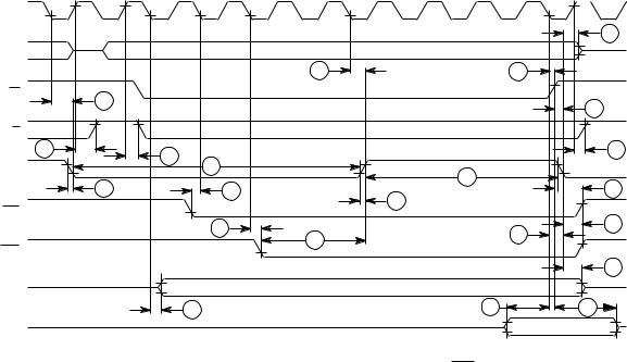
Figure 10-4. Read Cycle Timing Diagram
(Applies To All Processors Except The MC68EC000)
MOTOROLA |
M68000 8-/16-/32-BIT MICROPROCESSORS USER'S MANUAL |
10-13 |
CLK
FC2-FC0
A23-A1
AS
LDS / UDS
R/W
DTACK
DATA OUT
BERR / BR (NOTE 2)
HALT / RESET
ASYNCHRONOUS INPUTS (NOTE 1)
S0 |
|
S1 |
S2 |
S3 |
S4 |
S5 |
S6 |
S7 |
|
|
|
6A |
|
|
|
|
|
|
|
8 |
|
|
|
|
|
|
|
|
|
6 |
|
|
|
|
|
|
|
7 |
|
|
|
|
|
12 |
|
|
15 |
|
|
|
14 |
|
|
|
|
|
|
|
|
|
|
|
|
13 |
9 |
|
|
|
9 |
|
|
|
|
11 |
|
|
|
|
||
|
|
|
|
|
|
|
||
|
|
|
|
|
|
|
|
|
|
|
11A |
|
|
|
|
|
|
|
|
|
|
20A |
|
14A |
|
|
|
17 |
|
|
|
|
|
||
|
|
20 |
|
|
|
|
||
|
|
|
|
|
|
|
|
|
|
|
18 |
21 |
22 |
|
|
|
|
|
|
|
21A |
|
|
47 |
|
28 |
|
|
|
55 |
|
|
|
|
|
|
|
|
26 |
|
|
|
|
|
|
|
7 |
23 |
|
|
|
|
53 |
|
|
|
48 |
|
|
|
25 |
|
|
|
|
|
|
|
|
||
|
|
|
|
|
47 |
|
|
30 |
|
|
|
47 |
|
|
47 |
|
|
|
|
|
|
|
|
|
|
|
|
|
32 |
|
|
32 |
|
|
|
|
|
|
|
56 |
|
|
|
|
|
|
|
|
|
|
47 |
|
|
NOTES:
1. Timing measurements are referenced to and from a low voltage of 0.8 V and a high voltage of 2.0 V,
unless otherwise noted. The voltage swing through this range should start outside and pass through the range such that the rise or fall is linear between 0.8 V and 2.0 V.
2. Because of loading variations, R/W may be valid after AS even though both are initiated by the rising edge of S2 (specification #20A).
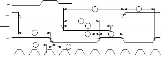
Figure 10-5. Write Cycle Timing Diagram
(Applies To All Processors Except The MC68EC000)
10-14 |
M68000 8-/16-/32-BIT MICROPROCESSORS USER'S MANUAL |
MOTOROLA |
10.11 AC ELECTRICAL SPECIFICATIONS—MC68000 TO M6800
PERIPHERAL (VCC = 5.0 Vdc ±5%; GND=0 Vdc; TA = TL TO TH; refer to figures 10-6) (Applies To All Processors Except The MC68EC000)
Num |
Characteristic |
8 MHz* |
10 MHz* |
12.5 MHz* |
16.67 MHz |
16 MHz |
20 MHz •• |
Unit |
|||||||
|
`12F' |
||||||||||||||
|
|
|
|
|
|
|
|
|
|
|
|
|
|
||
|
|
Min |
Max |
Min |
Max |
Min |
Max |
|
Min |
Max |
Min |
Max |
Min |
Max |
|
121 |
Clock Low to AS, DS Negated |
— |
62 |
— |
50 |
— |
40 |
— |
40 |
3 |
30 |
3 |
25 |
ns |
|
181 |
Clock High to R/W High |
0 |
55 |
0 |
45 |
0 |
40 |
|
0 |
40 |
0 |
30 |
0 |
25 |
ns |
|
(Read) |
|
|
|
|
|
|
|
|
|
|
|
|
|
|
201 |
Clock High to R/W Low |
0 |
55 |
0 |
45 |
0 |
40 |
|
0 |
40 |
0 |
30 |
0 |
25 |
ns |
|
(Write) |
|
|
|
|
|
|
|
|
|
|
|
|
|
|
23 |
Clock Low to Data-Out Valid |
— |
62 |
— |
50 |
— |
50 |
— |
50 |
— |
30 |
— |
25 |
ns |
|
|
(Write) |
|
|
|
|
|
|
|
|
|
|
|
|
|
|
27 |
Data-In Valid to Clock Low |
10 |
— |
10 |
— |
10 |
— |
7 |
— |
5 |
— |
5 |
— |
ns |
|
|
(Setup Time on Read) |
|
|
|
|
|
|
|
|
|
|
|
|
|
|
29 |
AS, DS Negated to Data-In |
0 |
— |
0 |
— |
0 |
— |
0 |
— |
0 |
— |
0 |
— |
ns |
|
|
Invalid (Hold Time on Read) |
|
|
|
|
|
|
|
|
|
|
|
|
|
|
40 |
Clock Low to VMA Asserted |
— |
70 |
— |
70 |
— |
70 |
— |
50 |
— |
50 |
— |
40 |
ns |
|
41 |
Clock Low to E Transition |
— |
55 |
— |
45 |
— |
35 |
— |
35 |
— |
35 |
— |
30 |
ns |
|
42 |
E Output Rise and Fall Time |
— |
15 |
— |
15 |
— |
15 |
— |
15 |
— |
15 |
— |
12 |
ns |
|
43 |
VMA Asserted to E High |
200 |
— |
150 |
— |
90 |
— |
80 |
— |
80 |
— |
60 |
— |
ns |
|
44 |
AS, DS Negated to VPA |
0 |
120 |
0 |
90 |
0 |
70 |
|
0 |
50 |
0 |
50 |
0 |
42 |
ns |
|
Negated |
|
|
|
|
|
|
|
|
|
|
|
|
|
|
45 |
E Low to Control, Address |
30 |
— |
10 |
— |
10 |
— |
10 |
— |
10 |
— |
10 |
— |
ns |
|
|
Bus Invalid (Address Hold |
|
|
|
|
|
|
|
|
|
|
|
|
|
|
|
Time) |
|
|
|
|
|
|
|
|
|
|
|
|
|
|
47 |
Asynchronous Input Setup |
10 |
— |
10 |
— |
10 |
— |
10 |
— |
10 |
— |
5 |
— |
ns |
|
|
Time |
|
|
|
|
|
|
|
|
|
|
|
|
|
|
492 |
AS, DS, Negated to E Low |
-70 |
70 |
-55 |
55 |
-45 |
45 |
|
-35 |
35 |
-35 |
35 |
–30 |
30 |
ns |
50 |
E Width High |
450 |
— |
350 — 280 — 220 — 220 |
— |
190 |
— |
ns |
|
||||||
51 |
E Width Low |
700 |
— |
550 |
— |
440 — 340 — 340 |
— |
290 |
— |
ns |
|
||||
54 |
E Low to Data-Out Invalid |
30 |
— |
20 |
— |
15 |
— |
10 |
— |
10 |
— |
5 |
— |
ns |
|
*These specifications represent improvement over previously published specifications for the 8-, 10-, and 12.5-MHz MC68000 and are valid only for product bearing date codes of 8827 and later.
** This frequency applies only to MC68HC000 and MC68HC001.
NOTES: 1. For a loading capacitance of less than or equal to 50 pF, subtract 5 ns from the value given in the maximum columns.
2.The falling edge of S6 triggers both the negation of the strobes (AS and DS) and the falling edge of E. Either of these events can occur first, depending upon the loading on each signal. Specificaton
#49 indicates the absolute maximum skew that will occur between the rising edge of the strobes and the falling edge of the E clock.
MOTOROLA |
M68000 8-/16-/32-BIT MICROPROCESSORS USER'S MANUAL |
10-15 |
S0 |
S1 |
S2 |
S3 |
S4 |
w |
w |
w |
w |
w |
w |
w |
w |
w |
w |
w |
w |
S5 |
S6 |
S7 |
S0 |
CLK |
|
|
|
|
|
|
|
|
|
|
|
|
|
|
|
|
|
|
|
|
|
|
|
|
|
|
|
|
|
|
|
|
|
|
|
|
|
|
|
|
45 |
A23-A1 |
|
|
|
|
|
|
|
|
|
|
|
|
|
|
|
|
|
|
|
|
|
|
|
|
|
|
|
|
|
|
|
41 |
|
|
|
|
|
12 |
|
|
|
AS |
|
|
41 |
|
|
|
|
|
|
|
|
|
|
|
|
|
|
|
|
|
|
|
|
|
|
|
|
|
|
|
|
|
|
|
|
|
|
|
|
49 |
|
|
|
|
|
|
|
|
|
|
|
|
|
|
|
|
|
|
|
|
|
|
R/W |
|
|
|
|
|
|
|
|
|
|
|
|
|
|
|
|
|
|
|
|
18 |
|
|
|
|
|
20 |
|
|
|
|
|
|
|
|
|
|
|
|
|
18 |
|
|
|
|
|
|
51 |
|
|
|
|
|
|
|
|
|
|
|
|
|
|
E |
|
|
|
|
|
|
|
|
|
|
|
|
|
|
|
50 |
|
|
|
|
|
|
|
|
|
|
|
|
|
|
|
|
|
|
|
|
|
|
|
||
|
|
|
42 |
|
|
|
|
|
|
|
|
|
|
|
|
|
|
|
44 |
|
|
|
|
|
|
|
|
47 |
|
|
|
|
|
|
42 |
|
|
|
|
||
VPA |
|
|
|
|
|
|
|
|
|
|
|
|
|
|
|
|
|
|
|
|
|
|
|
|
|
|
|
|
|
|
|
|
|
|
|
|
|
|
|
45 |
|
|
|
|
|
|
|
|
40 |
|
|
|
|
|
|
|
|
|
41 |
|
|
|
|
|
|
|
|
|
|
|
|
|
43 |
|
|
|
|
|
|
|
|
||
|
|
|
|
|
|
|
|
|
|
|
|
|
|
|
|
|
|
|
||
VMA |
|
|
|
|
|
|
|
|
|
|
|
|
|
|
|
|
|
|
|
|
|
|
|
|
|
|
|
|
|
|
|
|
|
|
|
|
|
|
|
|
|
|
|
|
|
|
|
|
|
|
|
|
|
|
|
|
|
|
|
|
|
54 |
DATA OUT |
|
|
23 |
27 |
29 |
DATA IN |
|
|
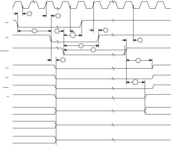
NOTE: This timing diagram is included for those who wish to design their own circuit to generate VMA. It shows the best case possible attainable
Figure 10-6. MC68000 to M6800 Peripheral Timing Diagram (Best Case)
(Applies To All Processors Except The MC68EC000)
10-16 |
M68000 8-/16-/32-BIT MICROPROCESSORS USER'S MANUAL |
MOTOROLA |
10.12 AC ELECTRICAL SPECIFICATIONS — BUS ARBITRATION (VCC=5.0
VDC±5%; GND=0 VDC, TA=TL TO TH; See Figure s 10-7 – 10-11) (Applies To All Processors Except The MC68EC000)
Num |
Characteristic |
8 MHz* |
10 MHz* |
12.5 MHz* |
16.67 MHz |
16 MHz |
20 MHz •• |
Unit |
|||||||
|
12F |
||||||||||||||
|
|
|
|
|
|
|
|
|
|
|
|
|
|
||
|
|
Min |
Max |
Min |
Max |
Min |
Max |
Min Max |
Min |
Max |
Min |
Max |
|
||
7 |
Clock High to Address, Data |
— |
80 |
— |
70 |
— |
60 |
— |
50 |
— |
50 |
— |
42 |
ns |
|
|
Bus High Impedance |
|
|
|
|
|
|
|
|
|
|
|
|
|
|
|
(Maximum) |
|
|
|
|
|
|
|
|
|
|
|
|
|
|
16 |
Clock High to Control Bus |
— |
80 |
— |
70 |
— |
60 |
— |
50 |
— |
50 |
— |
42 |
ns |
|
|
High Impedance |
|
|
|
|
|
|
|
|
|
|
|
|
|
|
33 |
Clock High to BG Asserted |
— |
62 |
— |
50 |
— |
40 |
0 |
40 |
0 |
30 |
0 |
25 |
ns |
|
34 |
Clock High to BG Negated |
— |
62 |
— |
50 |
— |
40 |
0 |
40 |
0 |
30 |
0 |
25 |
ns |
|
35 |
BR Asserted to BG Asserted |
1.5 |
3.5 |
1.5 |
3.5 |
1.5 |
3.5 |
1.5 |
|
3.5 |
1.5 |
3.5 |
1.5 |
3.5 |
Clks |
361 |
BR Negated to BG Negated |
1.5 |
3.5 |
1.5 |
3.5 |
1.5 |
3.5 |
1.5 |
|
3.5 |
1.5 |
3.5 |
1.5 |
3.5 |
Clks |
37 |
BGACK Asserted to BG |
1.5 |
3.5 |
1.5 |
3.5 |
1.5 |
3.5 |
1.5 |
|
3.5 |
1.5 |
3.5 |
1.5 |
3.5 |
Clks |
|
Negated |
|
|
|
|
|
|
|
|
|
|
|
|
|
|
37A2 |
BGACK Asserted to BR |
20 |
1.5 |
20 |
1.5 |
20 |
1.5 |
10 |
|
1.5 |
10 |
1.5 |
10 |
1.5 |
Clks/ |
|
Negated |
|
Clks |
|
Clks |
|
Clks |
|
Clks |
|
Clks |
|
Clks |
ns |
|
38 |
BG Asserted to Control, |
|
80 |
|
70 |
|
60 |
— |
50 |
— |
50 |
— |
42 |
ns |
|
|
Address, Data Bus High |
|
|
|
|
|
|
|
|
|
|
|
|
|
|
|
Impedance (AS Negated) |
|
|
|
|
|
|
|
|
|
|
|
|
|
|
39 |
BG Width Negated |
1.5 |
— |
1.5 |
— |
1.5 |
— |
1.5 |
— |
1.5 |
— |
1.5 |
— |
|
Clks |
46 |
BGACK Width Low |
1.5 |
— |
1.5 |
— |
1.5 |
— |
1.5 |
— |
1.5 |
— |
1.5 |
— |
|
Clks |
47 |
Asynchronous Input Setup |
10 |
— |
10 |
— |
10 |
— |
5 |
— |
5 |
— |
5 |
— |
ns |
|
|
Time |
|
|
|
|
|
|
|
|
|
|
|
|
|
|
57 |
BGACK Negated to AS, DS, |
1.5 |
— |
1.5 |
— |
1.5 |
— |
1.5 |
— |
1.5 |
— |
1.5 |
— |
Clks |
|
|
R/ W Driven |
|
|
|
|
|
|
|
|
|
|
|
|
|
|
57A |
BGACK Negated to FC, VMA |
1 |
— |
1 |
— |
1 |
— |
1 |
— |
1 |
— |
1 |
— |
Clks |
|
|
Driven |
|
|
|
|
|
|
|
|
|
|
|
|
|
|
581 |
BR Negated to AS, DS, R/W |
1.5 |
— |
1.5 |
— |
1.5 |
— |
1.5 |
— |
1.5 |
— |
1.5 |
— |
Clks |
|
|
Driven |
|
|
|
|
|
|
|
|
|
|
|
|
|
|
58A1 |
BR Negated to FC, VMA |
1 |
— |
1 |
— |
1 |
— |
1 |
— |
1 |
— |
1 |
— |
Clks |
|
|
Driven |
|
|
|
|
|
|
|
|
|
|
|
|
|
|
*These specifications represent improvement over previously published specifications for the 8-, 10-, and 12.5-MHz MC68000 and are valid only for product bearing date codes of 8827 and later.
** Applies only to the MC68HC000 and MC68HC001.
NOTES:
1.Setup time for the synchronous inputs BGACK, IPL0-IPL2 , and VPA guarantees their recognition at the next falling edge of the clock.
2.BR need fall at this time only in order to insure being recognized at the end of the bus cycle.
3.Timing measurements are referenced to and from a low voltage of 0.8 volt and a high voltage of 2.0 volts, unless otherwise noted. The voltage swing through this range should start outside and pass through the range such that the rise or fall will be lienar between 0.8 volt and 2.0 volts.
4.The processor will negate BG and begin driving the bus again if external arbitration logic negates BR before asserting BGACK.
5.The minimum value must be met to guarantee proper operation. If the maximum value is exceeded, BG may be reasserted.
MOTOROLA |
M68000 8-/16-/32-BIT MICROPROCESSORS USER'S MANUAL |
10-17 |
STROBES |
|
|
AND R/W |
37A |
36 |
|
||
BR |
|
|
|
37 |
|
BGACK |
46 |
|
|
|
|
35 |
34 |
39 |
|
||
BG |
|
|
33 |
38 |
|
|
|
|
CLK |
|
|
NOTE: Setup time to the clock (#47) for the asynchronous inputs BERR, BGACK, BR, DTACK, IPL2-IPL0, and VPA guarantees their recognition at the next falling edge of the clock.
Figure 10-7. Bus Arbitration Timing
(Applies To All Processors Except The MC68EC000)
10-18 |
M68000 8-/16-/32-BIT MICROPROCESSORS USER'S MANUAL |
MOTOROLA |

CLK |
|
|
47 |
33 |
|
|
|
|
BR |
|
|
35 |
47 |
34 |
|
|
37A |
BG |
|
47 |
|
|
37 |
1 |
|
46 |
BGACK |
|
|
|
38 |
57 |
AS |
|
|
DS |
|
57A |
|
|
|
VMA |
|
|
R/W |
|
|
FC2-FC0 |
|
|
A19-A0 |
|
|
D7-D0
NOTES: Waveform measurements for all inputs and outputs are specified at: logic high 2.0 V, logic low = 0.8 V. 1. MC68008 52-Pin Version only.
Figure 10-8. Bus Arbitration Timing
(Applies To All Processors Except The MC68EC000)
MOTOROLA |
M68000 8-/16-/32-BIT MICROPROCESSORS USER'S MANUAL |
10-19 |
CLK |
|
|
47 |
33 |
|
|
|
|
BR |
|
|
35 |
47 |
34 |
|
|
37A |
BG |
|
47 |
|
|
37 |
1 |
|
46 |
BGACK |
|
|
|
38 |
57 |
AS |
|
|
DS |
|
57A |
|
|
|
VMA |
|
|
R/W |
|
|
FC2-FC0 |
|
|
A19-A0 |
|
|
D7-D0
NOTES: Waveform measurements for all inputs and outputs are specified at: logic high 2.0 V, logic low = 0.8 V. 1. MC68008 52-Pin Version only.
Figure 10-9. Bus Arbitration Timing — Idle Bus Case
(Applies To All Processors Except The MC68EC000)
10-20 |
M68000 8-/16-/32-BIT MICROPROCESSORS USER'S MANUAL |
MOTOROLA |
CLK |
|
|
47 |
33 |
|
|
|
|
BR |
|
|
35 |
47 |
34 |
|
|
37A |
BG |
|
47 |
|
|
37 |
1 |
|
46 |
BGACK |
|
|
|
16 |
57 |
AS |
|
|
DS |
|
57A |
|
|
|
VMA |
|
|
R/W |
|
|
FC2-FC0 |
|
|
|
7 |
|
A19-A0 |
|
|
D7-D0 |
|
|
NOTE: Waveform measurements for all inputs and outputs are specified at: logic high 2.0 V, logic low = 0.8 V. 1 MC68008 52-Pin Version Only.
Figure 10-10. Bus Arbitration Timing — Active Bus Case
(Applies To All Processors Except The MC68EC000)
MOTOROLA |
M68000 8-/16-/32-BIT MICROPROCESSORS USER'S MANUAL |
10-21 |
CLK |
|
|
|
47 |
|
|
|
|
33 |
|
|
BR |
|
|
|
35 |
39 |
39 |
36 |
BG |
|
|
|
|
37 |
37 |
|
1 |
46 |
46 |
|
BGACK |
|
|
|
|
38 |
|
58 |
AS |
|
|
|
DS |
|
|
57A |
|
|
|
|
VMA |
|
|
|
R/W |
|
|
|
FC2-FC0
A19-A0
D7-D0
NOTES: Waveform measurements for all inputs and outputs are specified at: logic high 2.0 V, logic low = 0.8 V. 1. MC68008 52-Pin Version only.
Figure 10-11. Bus Arbitration Timing — Multiple Bus Request
(Applies To All Processors Except The MC68EC000)
10-22 |
M68000 8-/16-/32-BIT MICROPROCESSORS USER'S MANUAL |
MOTOROLA |