

SECTION 5
16-BIT BUS OPERATION
The following paragraphs describe control signal and bus operation for 16-bit bus operations during data transfer operations, bus arbitration, bus error and halt conditions, and reset operation. The 16-bit bus operation devices are the MC68000, MC68HC000,
MC68010, and the MC68HC001 and MC68EC000 in 16-bit mode. The MC68HC001 and
MC68EC000 select 16-bit mode by pulling mode high or leave it floating during reset.
5.1 DATA TRANSFER OPERATIONS
Transfer of data between devices involves the following signals:
1.Address bus A1 through highest numbered address line
2.Data bus D0 through D15
3.Control signals
The address and data buses are separate parallel buses used to transfer data using an asynchronous bus structure. In all cases, the bus master must deskew all signals it issues at both the start and end of a bus cycle. In addition, the bus master must deskew the acknowledge and data signals from the slave device.
The following paragraphs describe the read, write, read-modify-write, and CPU space cycles. The indivisible read-modify-write cycle implements interlocked multiprocessor communications. A CPU space cycle is a special processor cycle.
5.1.1 Read Cycle
During a read cycle, the processor receives either one or two bytes of data from the memory or from a peripheral device. If the instruction specifies a word or long-word operation, the MC68000, MC68HC000, MC68HC001, MC68EC000, or MC68010 processor reads both upper and lower bytes simultaneously by asserting both upper and lower data strobes. When the instruction specifies byte operation, the processor uses the internal A0 bit to determine which byte to read and issues the appropriate data strobe. When A0 equals zero, the upper data strobe is issued; when A0 equals one, the lower data strobe is issued. When the data is received, the processor internally positions the byte appropriately.
The word read-cycle flowchart is shown in Figure 5-1 and the byte read-cycle flowchart is shown in Figure 5-2. The read and write cycle timing is shown in Figure 5-3 and the word and byte read-cycle timing diagram is shown in Figure 5-4.
MOTOROLA |
M68000 8-/16-/32-BIT MICROPROCESSORS USER'S MANUAL |
5-1 |
BUS MASTER
ADDRESS THE DEVICE
1)SET R/W TO READ
2)PLACE FUNCTION CODE ON FC2–FC0
3)PLACE ADDRESS ON A23–A1
4)ASSERT ADDRESS STROBE (AS)
5)ASSERT UPPER DATA STROBE (UDS) AND LOWER DATA STROBE (LDS)
ACQUIRE THE DATA
1)LATCH DATA
2)NEGATE UDS AND LDS
3)NEGATE AS
START NEXT CYCLE
SLAVE
INPUT THE DATA
1)DECODE ADDRESS
2)PLACE DATA ON D15–D0
3)ASSERT DATA TRANSFER ACKNOWLEDGE (DTACK)
TERMINATE THE CYCLE
1)REMOVE DATA FROM D15–D0
2)NEGATE DTACK
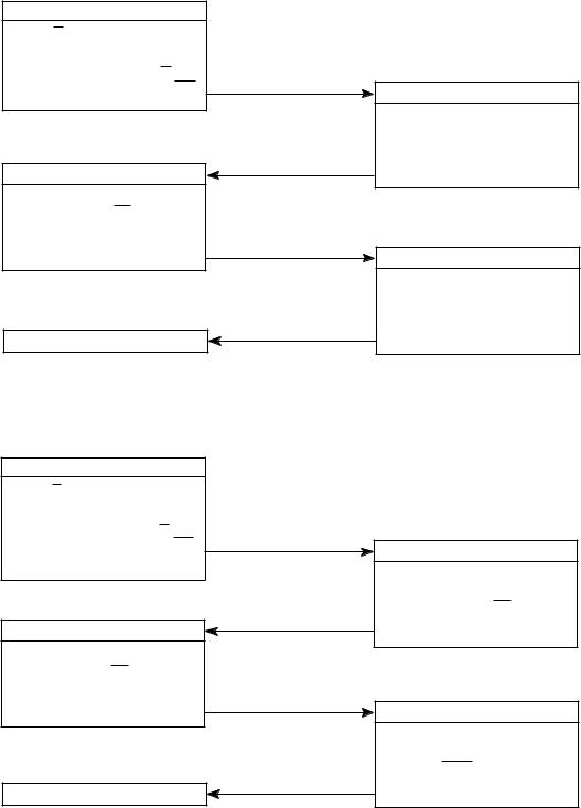
Figure 5-1. Word Read-Cycle Flowchart
BUS MASTER
ADDRESS THE DEVICE
1)SET R/W TO READ
2)PLACE FUNCTION CODE ON FC2–FC0
3)PLACE ADDRESS ON A23-A1
4)ASSERT ADDRESS STROBE (AS)
5)ASSERT UPPER DATA STROBE (UDS) OR LOWER DATA STROBE (LDS) (BASED ON INTERNAL A0)
ACQUIRE THE DATA
1)LATCH DATA
2)NEGATE UDS AND LDS
3)NEGATE AS
START NEXT CYCLE
SLAVE
INPUT THE DATA
1)DECODE ADDRESS
2)PLACE DATA ON D7–D0 OR D15–D8 (BASED ON UDS OR LDS)
3)ASSERT DATA TRANSFER ACKNOWLEDGE (DTACK)
TERMINATE THE CYCLE
1)REMOVE DATA FROM D7–D0 OR D15–D8
2)NEGATE DTACK
Figure 5-2. Byte Read-Cycle Flowchart
5-2 |
M68000 8-/16-/32-BIT MICROPROCESSORS USER'S MANUAL |
MOTOROLA |
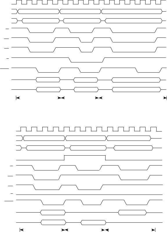
S0 S1 S2 S3 S4 S5 S6 S7 S0 S1 S2 S3 S4 S5 S6 S7 S0 S1 S2 S3 S4 w w w w S5 S6 S7
CLK
FC2–FC0
A23–A1
AS
UDS
LDS
R/W
DTACK
D15–D8
D7–D0
|
|
|
|
|
|
|
|
|
|
|
|
|
|
|
|
|
|
|
|
|
|
|
|
|
|
|
|
|
|
READ |
|
|
|
|
|
|
|
|
WRITE |
|
|
|
|
|
|
|
|
2 WAIT STATE READ |
|
||||||
|
|
|
|
|
|
|
|
|
|
|
|
|
|
|
|
|
|
|
|||||||||
|
Figure 5-3. Read and Write-Cycle Timing Diagram |
|
|
||||||||||||||||||||||||
S0 |
S1 |
S2 |
S3 |
S4 |
S5 |
S6 |
S7 |
S0 |
S1 |
S2 |
S3 |
S4 |
S5 |
S6 |
S7 |
S0 |
S1 |
S2 |
S3 |
S4 |
S5 |
S6 |
S7 |
||||
CLK
FC2–FC0
A23–A1
A0 *
AS
UDS
LDS
R/W
DTACK
D15–D8
D7–D0
|
|
|
|
|
|
|
READ |
|
WRITE |
|
READ |
||
*Internal Signal Only
Figure 5-4. Word and Byte Read-Cycle Timing Diagram
MOTOROLA |
M68000 8-/16-/32-BIT MICROPROCESSORS USER'S MANUAL |
5-3 |
A bus cycle consists of eight states. The various signals are asserted during specific states of a read cycle, as follows:
STATE 0 The read cycle starts in state 0 (S0). The processor places valid function codes on FC0–FC2 and drives R/W high to identify a read cycle.
STATE 1 Entering state 1 (S1), the processor drives a valid address on the address bus.
STATE 2 On the rising edge of state 2 (S2), the processor asserts AS and UDS, LDS, or DS.
STATE 3 During state 3 (S3), no bus signals are altered.
STATE 4 During state 4 (S4), the processor waits for a cycle termination signal (DTACK or BERR) or VPA, an M6800 peripheral signal. When VPA is asserted during S4, the cycle becomes a peripheral cycle (refer to
Appendix B M6800 Peripheral Interface). If neither termination signal is asserted before the falling edge at the end of S4, the processor inserts wait states (full clock cycles) until either DTACK or BERR is asserted.
STATE 5 During state 5 (S5), no bus signals are altered.
STATE 6 During state 6 (S6), data from the device is driven onto the data bus.
STATE 7 On the falling edge of the clock entering state 7 (S7), the processor latches data from the addressed device and negates AS, U D S, and LDS. At the rising edge of S7, the processor places the address bus in the highimpedance state. The device negates DTACK or BERR at this time.
NOTE
During an active bus cycle, VPA and BERR are sampled on every falling edge of the clock beginning with S4, and data is latched on the falling edge of S6 during a read cycle. The bus cycle terminates in S7, except when BERR is asserted in the absence of DTACK. In that case, the bus cycle terminates one clock cycle later in S9.
5.1.2 Write Cycle
During a write cycle, the processor sends bytes of data to the memory or peripheral device. If the instruction specifies a word operation, the processor issues both UDS and LDS and writes both bytes. When the instruction specifies a byte operation, the processor uses the internal A0 bit to determine which byte to write and issues the appropriate data strobe. When the A0 bit equals zero, UDS is asserted; when the A0 bit equals one, LDS is asserted.
5-4 |
M68000 8-/16-/32-BIT MICROPROCESSORS USER'S MANUAL |
MOTOROLA |
The word and byte write-cycle timing diagram and flowcharts in Figures 5-5, 5-6, and 5-7 applies directly to the MC68000, the MC68HC000, the MC68HC001 (in 16-bit mode), the
MC68EC000 (in 16-bit mode), and the MC68010.
BUS MASTER
ADDRESS THE DEVICE
1)PLACE FUNCTION CODE ON FC2–FC0
2)PLACE ADDRESS ON A23–A1
3)ASSERT ADDRESS STROBE (AS)
4)SET R/W TO WRITE
5)PLACE DATA ON D15–D0
6)ASSERT UPPER DATA STROBE (UDS) AND LOWER DATA STROBE (LDS)
TERMINATE OUTPUT TRANSFER
1)NEGATE UDS AND LDS
2)NEGATE AS
3)REMOVE DATA FROM D15–D0
4)SET R/W TO READ
SLAVE
INPUT THE DATA
1)DECODE ADDRESS
2)STORE DATA ON D15–D0
3)ASSERT DATA TRANSFER ACKNOWLEDGE (DTACK)
TERMINATE THE CYCLE
1) NEGATE DTACK
START NEXT CYCLE
Figure 5-5. Word Write-Cycle Flowchart
BUS MASTER
ADDRESS THE DEVICE
1)PLACE FUNCTION CODE ON FC2–FC0
2)PLACE ADDRESS ON A23–A1
3)ASSERT ADDRESS STROBE (AS)
4)SET R/W TO WRITE
5)PLACE DATA ON D0–D7 OR D15–D8
(ACCORDING TO INTERNAL A0)
6)ASSERT UPPER DATA STROBE (UDS) OR LOWER DATA STROBE (LDS)
(BASED ON INTERNAL A0)
TERMINATE OUTPUT TRANSFER
1)NEGATE UDS AND LDS
2)NEGATE AS
3)REMOVE DATA FROM D7-D0 OR D15-D8
4) SET R/W TO READ
START NEXT CYCLE
SLAVE
INPUT THE DATA
1)DECODE ADDRESS
2)STORE DATA ON D7–D0 IF LDS IS ASSERTED. STORE DATA ON D15–D8 IF UDS IS ASSERTED
3)ASSERT DATA TRANSFER ACKNOWLEDGE (DTACK)
TERMINATE THE CYCLE
1) NEGATE DTACK
Figure 5-6. Byte Write-Cycle Flowchart
MOTOROLA |
M68000 8-/16-/32-BIT MICROPROCESSORS USER'S MANUAL |
5-5 |
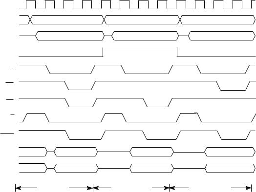
S0 |
S1 |
S2 |
S3 |
S4 |
S5 |
S6 |
S7 |
S0 |
S1 |
S2 |
S3 |
S4 |
S5 |
S6 |
S7 |
S0 |
S1 |
S2 |
S3 |
S4 |
S5 |
S6 |
S7 |
CLK |
|
|
|
|
|
|
|
|
|
|
|
|
|
|
|
|
|
|
|
|
|
|
|
FC2–FC0 |
|
|
|
|
|
|
|
|
|
|
|
|
|
|
|
|
|
|
|
|
|
|
|
A23–A1 |
|
|
|
|
|
|
|
|
|
|
|
|
|
|
|
|
|
|
|
|
|
|
|
A0* |
|
|
|
|
|
|
|
|
|
|
|
|
|
|
|
|
|
|
|
|
|
|
|
AS |
|
|
|
|
|
|
|
|
|
|
|
|
|
|
|
|
|
|
|
|
|
|
|
UDS |
|
|
|
|
|
|
|
|
|
|
|
|
|
|
|
|
|
|
|
|
|
|
|
LDS |
|
|
|
|
|
|
|
|
|
|
|
|
|
|
|
|
|
|
|
|
|
|
|
R/W |
|
|
|
|
|
|
|
|
|
|
|
|
|
|
|
|
|
|
|
|
|
|
|
DTACK |
|
|
|
|
|
|
|
|
|
|
|
|
|
|
|
|
|
|
|
|
|
|
|
D15–D8 |
|
|
|
|
|
|
|
|
|
|
|
|
|
|
|
|
|
|
|
|
|
|
|
D7–D0 |
|
|
|
|
|
|
|
|
|
|
|
|
|
|
|
|
|
|
|
|
|
|
|
*INTERNAL SIGNAL ONLY |
|
|
|
|
|
|
|
|
|
|
|
|
|
|
|
|
|
|
|
|
|
||
|
WORD WRITE |
|
|
|
|
ODD BYTE WRITE |
|
|
|
|
EVEN BYTE WRITE |
|
|
||||||||||
Figure 5-7. Word and Byte Write-Cycle Timing Diagram
The descriptions of the eight states of a write cycle are as follows:
STATE 0 The write cycle starts in S0. The processor places valid function codes on FC2–FC0 and drives R/W high (if a preceding write cycle has left R/W low).
STATE 1 Entering S1, the processor drives a valid address on the address bus.
STATE 2 On the rising edge of S2, the processor asserts AS and drives R/W low.
STATE 3 During S3, the data bus is driven out of the high-impedance state as the data to be written is placed on the bus.
STATE 4 At the rising edge of S4, the processor asserts U D S , or LDS. The processor waits for a cycle termination signal (DTACK or BERR) or VPA, an M6800 peripheral signal. When VPA is asserted during S4, the cycle becomes a peripheral cycle (refer to Appendix B M6800 Peripheral Interface. If neither termination signal is asserted before the falling edge at the end of S4, the processor inserts wait states (full clock cycles) until either DTACK or BERR is asserted.
STATE 5 During S5, no bus signals are altered.
STATE 6 During S6, no bus signals are altered.
5-6 |
M68000 8-/16-/32-BIT MICROPROCESSORS USER'S MANUAL |
MOTOROLA |

STATE 7 On the falling edge of the clock entering S7, the processor negates AS,
UDS, or LDS. As the clock rises at the end of S7, the processor places the address and data buses in the high-impedance state, and drives R/W high. The device negates DTACK or BERR at this time.
5.1.3 Read-Modify-Write Cycle.
The read-modify-write cycle performs a read operation, modifies the data in the arithmetic logic unit, and writes the data back to the same address. The address strobe ( AS) remains asserted throughout the entire cycle, making the cycle indivisible. The test and set (TAS) instruction uses this cycle to provide a signaling capability without deadlock between processors in a multiprocessing environment. The TAS instruction (the only instruction that uses the read-modify-write cycle) only operates on bytes. Thus, all read-modify-write cycles are byte operations. The read-modify-write flowchart shown in Figure 5-8 and the timing diagram in Figure 5-9, applies to the MC68000, the MC68HC000, the MC68HC001 (in 16-bit mode), the MC68EC000 (in 16-bit mode), and the MC68010.
BUS MASTER
ADDRESS THE DEVICE
1)SET R/W TO READ
2)PLACE FUNCTION CODE ON FC2–FC0
3)PLACE ADDRESS ON A23–A1
4)ASSERT ADDRESS STROBE (AS)
5)ASSERT UPPER DATA STROBE (UDS) OR LOWER DATA STROBE (LDS)
ACQUIRE THE DATA
1) LATCH DATA
1) NEGATE UDS AND LDS
2) START DATA MODIFICATION
START OUTPUT TRANSFER
1)SET R/W TO WRITE
2)PLACE DATA ON D7–D0 OR D15–D8
3)ASSERT UPPER DATA STROBE (UDS)
OR LOWER DATA STROBE (LDS)
TERMINATE OUTPUT TRANSFER
1)NEGATE UDS OR LDS
2)NEGATE AS
3)REMOVE DATA FROM D7–D0 OR D15–D8
4)SET R/W TO READ
SLAVE
INPUT THE DATA
1)DECODE ADDRESS
2)PLACE DATA ON D7–D0 OR D15–D0
3)ASSERT DATA TRANSFER ACKNOWLEDGE (DTACK)
TERMINATE THE CYCLE
1)REMOVE DATA FROM D7–D0 OR D15–D8
2)NEGATE DTACK
INPUT THE DATA
1)STORE DATA ON D7–D0 OR D15–D8
2)ASSERT DATA TRANSFER ACKNOWLEDGE (DTACK)
TERMINATE THE CYCLE
1) NEGATE DTACK
START NEXT CYCLE
Figure 5-8. Read-Modify-Write Cycle Flowchart
MOTOROLA |
M68000 8-/16-/32-BIT MICROPROCESSORS USER'S MANUAL |
5-7 |
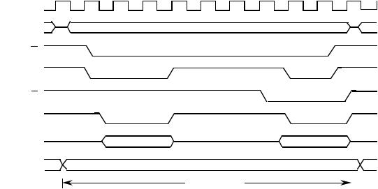
S0 |
S1 |
S2 |
S3 |
S4 |
S5 |
S6 |
S7 |
S8 |
S9 |
S10 |
S11 |
S12 |
S13 |
S14 |
S15 |
S16 |
S17 |
S18 |
S19 |
CLK
A23–A1
AS
UDS OR LDS
R/W
DTACK
D15–D8
FC2–FC0
INDIVISIBLE CYCLE
Figure 5-9. Read-Modify-Write Cycle Timing Diagram
The descriptions of the read-modify-write cycle states are as follows:
STATE 0 The read cycle starts in S0. The processor places valid function codes on FC2–FC0 and drives R/W high to identify a read cycle.
STATE 1 Entering S1, the processor drives a valid address on the address bus.
STATE 2 On the rising edge of S2, the processor asserts AS and UDS, or LDS.
STATE 3 During S3, no bus signals are altered.
STATE 4 During S4, the processor waits for a cycle termination signal (DTACK or BERR) or VPA, an M6800 peripheral signal. When VPA is asserted during S4, the cycle becomes a peripheral cycle (refer to Appendix B M6800 Peripheral Interface). If neither termination signal is asserted before the falling edge at the end of S4, the processor inserts wait states (full clock cycles) until either DTACK or BERR is asserted.
STATE 5 During S5, no bus signals are altered.
STATE 6 During S6, data from the device are driven onto the data bus.
STATE 7 On the falling edge of the clock entering S7, the processor accepts data from the device and negates U D S , and LDS. The device negates DTACK or BERR at this time.
STATES 8–11
The bus signals are unaltered during S8–S11, during which the arithmetic logic unit makes appropriate modifications to the data.
5-8 |
M68000 8-/16-/32-BIT MICROPROCESSORS USER'S MANUAL |
MOTOROLA |