

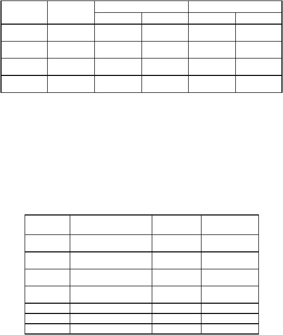
7.7 BIT MANIPULATION INSTRUCTION EXECUTION TIMES
Table 7-9 lists the timing data for the bit manipulation instructions. The total number of clock periods, the number of read cycles, and the number of write cycles are shown in the previously described format. The number of clock periods, the number of read cycles, and the number of write cycles, respectively, must be added to those of the effective address calculation where indicated by a plus sign (+).
Table 7-9. Bit Manipulation Instruction Execution Times
|
|
Dynamic |
|
|
Static |
Instruction |
Size |
Register |
Memory |
Register |
Memory |
BCHG |
Byte |
— |
12(2/1)+ |
— |
20(4/1)+ |
|
Long |
12(2/0)* |
— |
20(4/0)* |
— |
BCLR |
Byte |
— |
12(2/1)+ |
— |
20(4/1)+ |
|
Long |
14(2/0)* |
— |
22(4/0)* |
— |
BSET |
Byte |
— |
12(2/1)+ |
— |
20(4/1)+ |
|
Long |
12(2/0)* |
— |
20(4/0)* |
— |
BTST |
Byte |
— |
8(2/0)+ |
— |
16(4/0)+ |
|
Long |
10(2/0) |
|
18(4/0) |
— |
+Add effective address calculation time.
*Indicates maximum value; data addressing mode only.
7.8CONDITIONAL INSTRUCTION EXECUTION TIMES
Table 7-10 lists the timing data for the conditional instructions. The total number of clock periods, the number of read cycles, and the number of write cycles are shown in the previously described format. The number of clock periods, the number of read cycles, and the number of write cycles, respectively, must be added to those of the effective address calculation where indicated by a plus sign (+).
Table 7-10. Conditional Instruction Execution Times
|
|
Trap or Branch |
Trap or Branch |
Instruction |
Displacement |
Taken |
Not Taken |
Bcc |
Byte |
18(4/0) |
12(2/0) |
|
Word |
18(4/0) |
20(4/0) |
BRA |
Byte |
18(4/0) |
— |
|
Word |
18(4/0) |
— |
BSR |
Byte |
34(4/4) |
— |
|
Word |
34(4/4) |
— |
DBcc |
CC True |
— |
20(4/0) |
|
CC False |
18(4/0) |
26(6/0) |
CHK |
— |
68(8/6)+* |
14(2/0) |
TRAP |
— |
62(8/6) |
— |
TRAPV |
— |
66(10/6) |
8(2/0) |
+Add effective address calculation time for word operand. * Indicates maximum base value.
MOTOROLA |
M68000 8-/16-/32-BIT MICROPROCESSORS USER'S MANUAL |
7-7 |

7.9JMP, JSR, LEA, PEA, AND MOVEM INSTRUCTION EXECUTION TIMES
Table 7-11 lists the timing data for the jump (JMP), jump to subroutine (JSR), load effective address (LEA), push effective address (PEA), and move multiple registers
(MOVEM) instructions. The total number of clock periods, the number of read cycles, and the number of write cycles are shown in the previously described format.
Table 7-11. JMP, JSR, LEA, PEA, and MOVEM Instruction Execution Times
Instruction |
Size |
(An) |
(An)+ |
–(An) |
(d 16 ,An) |
(d 8,An,Xn)+ |
(xxx).W |
(xxx).L |
(d 16 PC) |
(d 8, PC, Xn)* |
||
JMP |
— |
16 (4/0) |
— |
— |
18 (4/0) |
22 (4/0) |
18 (4/0) |
24 (6/0) |
18 |
(4/0) |
22 |
(4/0) |
JSR |
— |
32 (4/4) |
— |
— |
34 (4/4) |
38 (4/4) |
34 (4/4) |
40 (6/4) |
34 |
(4/4) |
32 |
(4/4) |
LEA |
— |
8(2/0) |
— |
— |
16 (4/0) |
20 (4/0) |
16 (4/0) |
24 (6/0) |
16 |
(4/0) |
20 |
(4/0) |
PEA |
— |
24 (2/4) |
— |
— |
32 (4/4) |
36 (4/4) |
32 (4/4) |
40 (6/4) |
32 |
(4/4) |
36 |
(4/4) |
MOVEM |
Word |
24+8n |
24+8n |
— |
32+8n |
34+8n |
32+8n |
40+8n |
32+8n |
34+8n |
||
M → R |
|
(6+2n/0) |
(6+2n/0) |
|
(8+2n/0) |
(8+2n/0) |
(10+n/0) |
(10+2n/0) |
(8+2n/0) |
(8+2n/0) |
||
|
Long |
24+16n |
24+16n |
— |
32+16n |
34+16n |
32+16n |
40+16n |
32+16n |
34+16n |
||
|
|
(6+4n/0) |
(6+4n/0) |
|
(8+4n/0) |
(8+4n/0) |
(8+4n/0) |
(8+4n/0) |
(8+4n/0) |
(8+4n/0) |
||
MOVEM |
Word |
16+8n |
— |
16+8n |
24+8n |
26+8n |
24+8n |
32+8n |
|
— |
|
— |
R → M |
|
(4/2n) |
— |
(4/2n) |
(6/2n) |
(6/2n) |
(6/2n) |
(8/2n) |
|
— |
|
— |
|
Long |
16+16n |
— |
16+16n |
24+16n |
26+16n |
24+16n |
32+16n |
|
— |
|
— |
|
|
(4/4n) |
— |
(4/4n) |
(6/4n) |
|
(8/4n) |
(6/4n) |
|
— |
|
— |
n is the number of registers to move.
*The size of the index register (Xn) does not affect the instruction's execution time.
7.10 MULTIPRECISION INSTRUCTION EXECUTION TIMES
Table 7-12 lists the timing data for multiprecision instructions. The numbers of clock periods include the times to fetch both operands, perform the operations, store the results, and read the next instructions. The total number of clock periods, the number of read cycles, and the number of write cycles are shown in the previously described format.
The following notation applies in Table 7-12:
Dn — Data register operand
M — Memory operand
7-8 |
M68000 8-/16-/32-BIT MICROPROCESSORS USER'S MANUAL |
MOTOROLA |

Table 7-12. Multiprecision Instruction
Execution Times
Instruction |
Size |
op Dn, Dn |
op M, M |
ADDX |
Byte |
8(2/0) |
22(4/1) |
|
Word |
8(2/0) |
50(6/2) |
|
Long |
12(2/0) |
58(10/4) |
CMPM |
Byte, |
— |
16(4/0) |
|
Word |
— |
24(6/0) |
|
Long |
— |
40(10/0) |
SUBX |
Byte, \ |
8(2/0) |
22(4/1) |
|
Word |
8(2/0) |
50(6/2) |
|
Long |
12(2/0) |
58(10/4) |
ABCD |
Byte |
10(2/0) |
20(4/1) |
SBCD |
Byte |
10(2/0) |
20(4/1) |
7.11 MISCELLANEOUS INSTRUCTION EXECUTION TIMES
Tables 7-13 and 7-14 list the timing data for miscellaneous instructions. The total number of clock periods, the number of read cycles, and the number of write cycles are shown in the previously described format. The number of clock periods, the number of read cycles, and the number of write cycles, respectively, must be added to those of the effective address calculation where indicated by a plus sign (+).
MOTOROLA |
M68000 8-/16-/32-BIT MICROPROCESSORS USER'S MANUAL |
7-9 |

Table 7-13. Miscellaneous Instruction Execution Times
Instruction |
Register |
Memory |
ANDI to CCR |
32(6/0) |
— |
ANDI to SR |
32(6/0) |
— |
EORI to CCR |
32(6/0) |
— |
EORI to SR |
32(6/0) |
— |
EXG |
10(2/0) |
— |
EXT |
8(2/0) |
— |
LINK |
32(4/4) |
— |
MOVE to CCR |
18(4/0) |
18(4/0)+ |
MOVE to SR |
18(4/0) |
18(4/0)+ |
MOVE from SR |
10(2/0) |
16(2/2)+ |
MOVE to USP |
8(2/0) |
— |
MOVE from USP |
8(2/0) |
— |
NOP |
8(2/0) |
— |
ORI to CCR |
32(6/0) |
— |
ORI to SR |
32(6/0) |
— |
RESET |
136(2/0) |
— |
RTE |
40(10/0) |
— |
RTR |
40(10/0) |
— |
RTS |
32(8/0) |
— |
STOP |
4(0/0) |
— |
SWAP |
8(2/0) |
— |
TRAPV (No Trap) |
8(2/0) |
— |
UNLK |
24(6/0) |
— |
+Add effective address calculation time for word operand.
Table 7-14. Move Peripheral Instruction Execution Times
Instruction |
Size |
Register → Memory |
Memory → Register |
MOVEP |
Word |
24(4/2) |
24(6/0) |
|
Long |
32(4/4) |
32(8/0) |
+Add effective address calculation time.
7.12 EXCEPTION PROCESSING EXECUTION TIMES
Table 7-15 lists the timing data for exception processing. The numbers of clock periods include the times for all stacking, the vector fetch, and the fetch of the first instruction of the handler routine. The total number of clock periods, the number of read cycles, and the number of write cycles are shown in the previously described format. The number of clock
7-10 |
M68000 8-/16-/32-BIT MICROPROCESSORS USER'S MANUAL |
MOTOROLA |

periods, the number of read cycles, and the number of write cycles, respectively, must be added to those of the effective address calculation where indicated by a plus sign (+).
Table 7-15. Exception Processing
Execution Times
Exception |
Periods |
Address Error |
94(8/14) |
Bus Error |
94(8/14) |
CHK Instruction |
68(8/6)+ |
Divide by Zero |
66(8/6)+ |
Interrupt |
72(9/6)* |
Illegal Instruction |
62(8/6) |
Privilege Violation |
62(8/6) |
RESET** |
64(12/0) |
Trace |
62(8/6) |
TRAP Instruction |
62(8/6) |
TRAPV Instruction |
66(10/6) |
+Add effective address calculation time.
**Indicates the time from when RESET and HALT are first sampled as negated to when instruction execution starts.
MOTOROLA |
M68000 8-/16-/32-BIT MICROPROCESSORS USER'S MANUAL |
7-11 |