

shown in Figure 6-9. If the bus cycle is a read, the data at the fault address should be written to the images of the data input buffer, instruction input buffer, or both according to the data fetch (DF) and instruction fetch (IF) bits.* In addition, for read-modify-write cycles, the status register image must be properly set to reflect the read data if the fault occurred during the read portion of the cycle and the write operation (i.e., setting the most significant bit of the memory location) must also be performed. These operations are required because the entire read-modify-write cycle is assumed to have been completed by software. Once the cycle has been completed by software, the rerun (RR) bit in the special status word is set to indicate to the processor that it should not rerun the cycle when the RTE instruction is executed. If the RR bit is set when an RTE instruction executes, the MC68010 reads all the information from the stack, as usual.
15 |
14 |
13 |
12 |
11 |
10 |
9 |
8 |
7 |
3 |
2 |
0 |
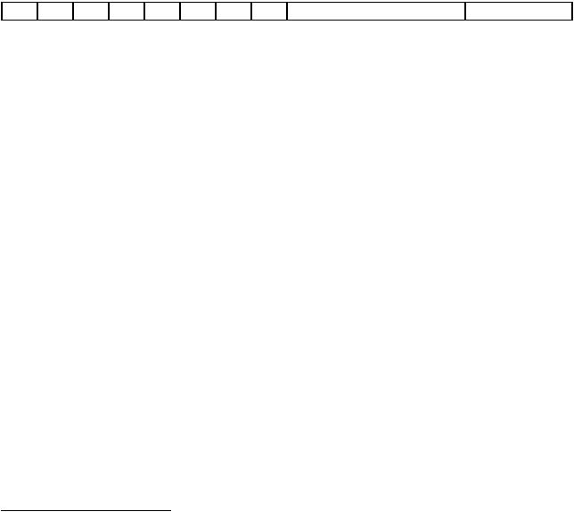
RR |
* |
I F |
DF |
RM |
HB |
BY |
RW |
* |
|
FC2–FC0 |
|
RR |
— Rerun flag; 0=processor rerun (default), 1=software rerun |
|
|
|
|||||||
IF |
— Instruction fetch to the instruction input buffer |
|
|
|
|
|
|||||
DF |
— Data fetch to the data input buffer |
|
|
|
|
|
|
||||
RM |
— Read-modify-write cycle |
|
|
|
|
|
|
|
|
||
HB — High-byte transfer from the data output buffer or to the data input buffer |
|
|
|
||||||||
BY — Byte-transfer flag; HB selects the high or low byte of the transfer register. If BY is clear, the transfer is word. |
|
||||||||||
RW |
— |
Read/write flag; 0=write, 1=read |
|
|
|
|
|
||||
FC — The function code used during the faulted access
*— These bits are reserved for future use by Motorola and will be zero when written by the MC68010.
Figure 6-9. Special Status Word Format
6.3.10 Address Error
An address error exception occurs when the processor attempts to access a word or longword operand or an instruction at an odd address. An address error is similar to an internally generated bus error. The bus cycle is aborted, and the processor ceases current processing and begins exception processing. The exception processing sequence is the same as that for a bus error, including the information to be stacked, except that the vector number refers to the address error vector. Likewise, if an address error occurs during the exception processing for a bus error, address error, or reset, the processor is halted.
On the MC68010, the address error exception stacks the same information stacked by a bus error exception. Therefore, the RTE instruction can be used to continue execution of the suspended instruction. However, if the RR flag is not set, the fault address is used when the cycle is retried, and another address error exception occurs. Therefore, the user must be certain that the proper corrections have been made to the stack image and user registers before attempting to continue the instruction. With proper software handling, the address error exception handler could emulate word or long-word accesses to odd addresses if desired.
*If the faulted access was a byte operation, the data should be moved from or to the least significant byte of the data output or input buffer images, unless the high-byte transfer (HB) bit is set. This condition occurs if a MOVEP instruction caused the fault during transfer of bits 8–15 of a word or long word or bits 24–31 of a long word.
MOTOROLA |
M68000 8-/16-/32-BIT MICROPROCESSORS USER’S MANUAL |
6-19 |
6.4 RETURN FROM EXCEPTION (MC68010)
In addition to returning from any exception handler routine on the MC68010, the RTE instruction resumes the execution of a suspended instruction by returning to the normal processing state after restoring all of the temporary register and control information stored during a bus error. For the RTE instruction to execute properly, the stack must contain valid and accessible data. The RTE instruction checks for data validity in two ways. First, the format/offset word is checked for a valid stack format code. Second, if the format code indicates the long stack format, the validity of the long stack data is checked as it is loaded into the processor. In addition, the data is checked for accessibility when the processor starts reading the long data. Because of these checks, the RTE instruction executes as follows:
1.Determine the stack format. This step is the same for any stack format and consists of reading the status register, program counter, and format/offset word. If the format code indicates a short stack format, execution continues at the new program counter address. If the format code is not an MC68010-defined stack format code, exception processing starts for a format error.
2.Determine data validity. For a long-stack format, the MC68010 begins to read the remaining stack data, checking for validity of the data. The only word checked for validity is the first of the 16 internal information words (SP + 26) shown in Figure 5-8. This word contains a processor version number (in bits 10–13) and proprietary internal information that must match the version number of the MC68010 attempting to read the data. This validity check is used to ensure that the data is properly interpreted by the RTE instruction. If the version number is incorrect for this processor, the RTE instruction is aborted and exception processing begins for a format error exception. Since the stack pointer is not updated until the RTE instruction has successfully read all the stack data, a format error occurring at this point does not stack new data over the previous bus error stack information.
3.Determine data accessibility. If the long-stack data is valid, the MC68010 performs a read from the last word (SP + 56) of the long stack to determine data accessibility. If this read is terminated normally, the processor assumes that the remaining words on the stack frame are also accessible. If a bus error is signaled before or during this read, a bus error exception is taken. After this read, the processor must be able to load the remaining data without receiving a bus error; therefore, if a bus error occurs on any of the remaining stack reads, the error becomes a double bus fault, and the MC68010 enters the halted state.
6-20 |
M68000 8-/16-/32-BIT MICROPROCESSORS USER'S MANUAL |
MOTOROLA |
SECTION 7
8-BIT INSTRUCTION EXECUTION TIMES
This section contains listings of the instruction execution times in terms of external clock
(CLK) periods for the MC68008 and MC68HC001/MC68EC000 in 8-bit mode. In this data, it is assumed that both memory read and write cycles consist of four clock periods. A longer memory cycle causes the generation of wait states that must be added to the total instruction times.
The number of bus read and write cycles for each instruction is also included with the timing data. This data is shown as
n(r/w)
where:
n is the total number of clock periods r is the number of read cycles
w is the number of write cycles
For example, a timing number shown as 18(3/1) means that 18 clock periods are required to execute the instruction. Of the 18 clock periods, 12 are used for the three read cycles (four periods per cycle). Four additional clock periods are used for the single write cycle, for a total of 16 clock periods. The bus is idle for two clock periods during which the processor completes the internal operations required for the instruction.
NOTE
The total number of clock periods (n) includes instruction fetch and all applicable operand fetches and stores.
7.1 OPERAND EFFECTIVE ADDRESS CALCULATION TIMES
Table 7-1 lists the numbers of clock periods required to compute the effective addresses for instructions. The totals include fetching any extension words, computing the address, and fetching the memory operand. The total number of clock periods, the number of read cycles, and the number of write cycles (zero for all effective address calculations) are shown in the previously described format.
MOTOROLA |
M68000 8-/16-/32-BIT MICROPROCESSORS USER'S MANUAL |
7-1 |

Table 7-1. Effective Address Calculation Times
|
Addressing Mode |
Byte |
Word |
Long |
|
Register |
|
|
|
Dn |
Data Register Direct |
0(0/0) |
0(0/0) |
0(0/0) |
An |
Address Register Direct |
0(0/0) |
0(0/0) |
0(0/0) |
|
Memory |
|
|
|
(An) |
Address Register Indirect |
4(1/0) |
8(2/0) |
16(4/0) |
(An)+ |
Address Register Indirect with Postincrement |
4(1/0) |
8(2/0) |
16(4/0) |
–(An) |
Address Register Indirect with Predecrement |
6(1/0) |
10(2/0) |
18(4/0) |
(d 16, An) |
Address Register Indirect with Displacement |
12(3/0) |
16(4/0) |
24(6/0) |
(d 8, An, Xn)* |
Address Register Indirect with Index |
14(3/0) |
18(4/0) |
26(6/0) |
(xxx).W |
Absolute Short |
12(3/0) |
16(4/0) |
24(6/0) |
(xxx).L |
Absolute Long |
20(5/0) |
24(6/0) |
32(8/0) |
(d 16, PC) |
Program Counter Indirect with Displacement |
12(3/0) |
16(3/0) |
24(6/0) |
(d 8, PC, Xn)* |
Program Counter Indirect with Index |
14(3/0) |
18(4/0) |
26(6/0) |
#<data> |
Immediate |
8(2/0) |
8(2/0) |
16(4/0) |
*The size of the index register (Xn) does not affect execution time.
7.2 MOVE INSTRUCTION EXECUTION TIMES
Tables 7-2, 7-3, and 7-4 list the numbers of clock periods for the move instructions. The totals include instruction fetch, operand reads, and operand writes. The total number of clock periods, the number of read cycles, and the number of write cycles are shown in the previously described format.
Table 7-2. Move Byte Instruction Execution Times
|
|
|
|
|
Destination |
|
|
|
|
Source |
Dn |
An |
(An) |
(An)+ |
–(An) |
(d16, An) |
(d8, An, Xn)* |
(xxx).W |
(xxx).L |
Dn |
8(2/0) |
8(2/0) |
12(2/1) |
12(2/1) |
12(2/1) |
20(4/1) |
22(4/1) |
20(4/1) |
28(6/1) |
An |
8(2/0) |
8(2/0) |
12(2/1) |
12(2/1) |
12(2/1) |
20(4/1) |
22(4/1) |
20(4/1) |
28(6/1) |
(An) |
12(3/0) |
12(3/0) |
16(3/1) |
16(3/1) |
16(3/1) |
24(5/1) |
26(5/1) |
24(5/1) |
32(7/1) |
(An)+ |
12(3/0) |
12(3/0) |
16(3/1) |
16(3/1) |
16(3/1) |
24(5/1) |
26(5/1) |
24(5/1) |
32(7/1) |
–(An) |
14(3/0) |
14(3/0) |
18(3/1) |
18(3/1) |
18(3/1) |
26(5/1) |
28(5/1) |
26(5/1) |
34(7/1) |
(d 16, An) |
20(5/0) |
20(5/0) |
24(5/1) |
24(5/1) |
24(5/1) |
32(7/1) |
34(7/1) |
32(7/1) |
40(9/1) |
(d 8, An, Xn)* |
22(5/0) |
22(5/0) |
26(5/1) |
26(5/1) |
26(5/1) |
34(7/1) |
36(7/1) |
34(7/1) |
42(9/1) |
(xxx).W |
20(5/0) |
20(5/0) |
24(5/1) |
24(5/1) |
24(5/1) |
32(7/1) |
34(7/1) |
32(7/1) |
40(9/1) |
(xxx).L |
28(7/0) |
28(7/0) |
32(7/1) |
32(7/1) |
32(7/1) |
40(9/1) |
42(9/1) |
40(9/1) |
48(11/1) |
(d 16, PC) |
20(5/0) |
20(5/0) |
24(5/1) |
24(5/1) |
24(5/1) |
32(7/1) |
34(7/1) |
32(7/1) |
40(9/1) |
(d 8, PC, Xn)* |
22(5/0) |
22(5/0) |
26(5/1) |
26(5/1) |
26(5/1) |
34(7/1) |
36(7/1) |
34(7/1) |
42(9/1) |
#<data> |
16(4/0) |
16(4/0) |
20(4/1) |
20(4/1) |
20(4/1) |
28(6/1) |
30(6/1) |
28(6/1) |
36(8/1) |
*The size of the index register (Xn) does not affect execution time.
7-2 |
M68000 8-/16-/32-BIT MICROPROCESSORS USER'S MANUAL |
MOTOROLA |