

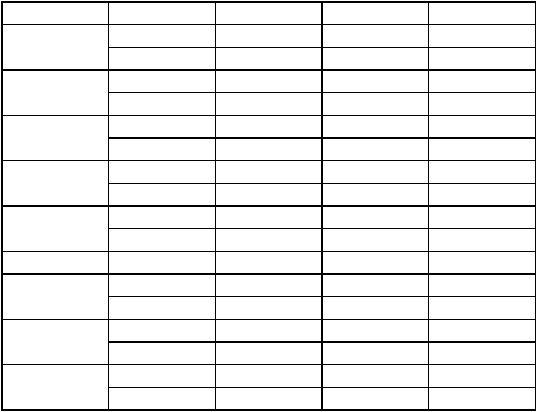
9.4 IMMEDIATE INSTRUCTION EXECUTION TIMES
The numbers of clock periods shown in Table 9-8 include the times to fetch immediate operands, perform the operations, store the results, and read the next operation. The total number of clock periods, the number of read cycles, and the number of write cycles are shown in the previously described format. The number of clock periods, the number of read cycles, and the number of write cycles, respectively, must be added to those of the effective address calculation where indicated by a plus sign (+).
In Tables 9-8, the following notation applies:
# — Immediate operand
Dn — Data register operand An — Address register operand M — Memory operand
Table 9-8. Immediate Instruction Execution Times
Instruction |
Size |
op #, Dn |
op #, An |
op #, M |
ADDI |
Byte, Word |
8(2/0) |
— |
12(2/1)+ |
|
Long |
14(3/0) |
— |
20(3/2)+ |
ADDQ |
Byte, Word |
4(1/0) |
4(1/0)* |
8(1/2)+ |
|
Long |
8(1/0) |
8(1/1) |
12(1/2)+ |
ANDI |
Byte, Word |
8(2/0) |
— |
12(2/1)+ |
|
Long |
14(3/0) |
— |
20(3/1)+ |
CMPI |
Byte, Word |
8(2/0) |
— |
8(2/0)+ |
|
Long |
12(3/0) |
— |
12(3/0)+ |
EORI |
Byte, Word |
8(2/0) |
— |
12(2/1)+ |
|
Long |
14(3/0) |
— |
20(3/2)+ |
MOVEQ |
Long |
4(1/0) |
— |
— |
ORI |
Byte, Word |
8(2/0) |
— |
12(2/1)+ |
|
Long |
14(3/0) |
— |
20(3/2)+ |
SUBI |
Byte, Word |
8(2/0) |
— |
12(2/1)+ |
|
Long |
14(3/0) |
— |
20(3/2)+ |
SUBQ |
Byte, Word |
4(1/0) |
4(1/0)* |
8(1/1)+ |
|
Long |
8(1/0) |
8(1/0) |
12(1/2)+ |
+Add effective address calculation time. *Word only.
9.5 SINGLE OPERAND INSTRUCTION EXECUTION TIMES
Tables 9-9, 9-10, and 9-11 list the timing data for the single operand instructions. The total number of clock periods, the number of read cycles, and the number of write cycles are shown in the previously described format. The number of clock periods, the number of read cycles, and the number of write cycles, respectively, must be added to those of the effective address calculation where indicated by a plus sign (+).
9-6 |
M68000 8-/16-/32-BIT MICROPROCESSORS USER'S MANUAL |
MOTOROLA |
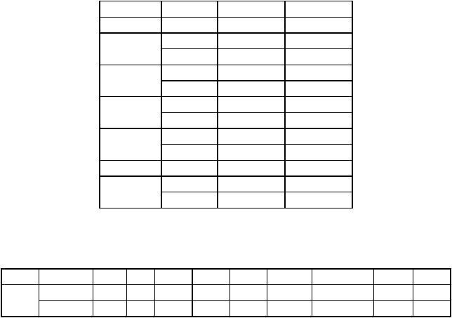
Table 9-9. Single Operand Instruction
Execution Times
Instruction |
Size |
Register |
Memory |
NBCD |
Byte |
6(1/0) |
8(1/1)+ |
NEG |
Byte, Word |
4(1/0) |
8(1/1)+ |
|
Long |
6(1/0) |
12(1/2)+ |
NEGX |
Byte, Word |
4(1/0) |
8(1/1)+ |
|
Long |
6(1/0) |
12(1/2)+ |
NOT |
Byte, Word |
4(1/0) |
8(1/1)+ |
|
Long |
6(1/0) |
12(1/2)+ |
Scc |
Byte, False |
4(1/0) |
8(1/1)+* |
|
Byte, True |
4(1/0) |
8(1/1)+* |
TAS |
Byte |
4(1/0) |
14(2/1)+* |
TST |
Byte, Word |
4(1/0) |
4(1/0)+ |
|
Long |
4(1/0) |
4(1/0)+ |
+Add effective address calculation time.
*Use nonfetching effective address calculation time.
Table 9-10. Clear Instruction Execution Times
|
Size |
Dn |
An |
(An) |
(An)+ |
–(An) |
(d 16 , An) |
(d 8, An, Xn)* |
(xxx).W |
(xxx).L |
CLR |
Byte, Word |
4(1/0) |
— |
8(1/1) |
8(1/1) |
10(1/1) |
12(2/1) |
16(2/1) |
12(2/1) |
16(3/1) |
|
Long |
6(1/0) |
— |
12(1/2) |
12(1/2) |
14(1/2) |
16(2/2) |
20(2/2) |
16(2/2) |
20(3/2) |
*The size of the index register (Xn) does not affect execution time.
MOTOROLA |
M68000 8-/16-/32-BIT MICROPROCESSORS USER’S MANUAL |
9-7 |
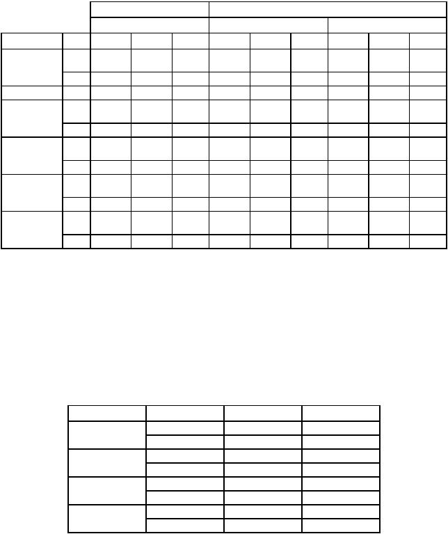
Table 9-11. Single Operand Instruction Loop Mode Execution Times
|
|
Loop Continued |
|
|
Loop Terminated |
|
|
|||
|
|
Valid Count, cc False |
Valid Count, cc True |
|
Expired Count |
|
||||
Instruction |
Size |
(An) |
(An)+ |
–(An) |
(An) |
(An)+ |
–(An) |
(An) |
(An)+ |
–(An) |
CLR |
Byte, |
10(0/1) |
10(0/1) |
12(0/1) |
18(2/1) |
18(2/1) |
20(2/0) |
16(2/1) |
16(2/1) |
18(2/1) |
|
Word |
|
|
|
|
|
|
|
|
|
|
Long |
14(0/2) |
14(0/2) |
16(0/2) |
22(2/2) |
22(2/2) |
24(2/2) |
20(2/2) |
20(2/2) |
22(2/2) |
NBCD |
Byte |
18(1/1) |
18(1/1) |
20(1/1) |
24(3/1) |
24(3/1) |
26(3/1) |
22(3/1) |
22(3/1) |
24(3/1) |
NEG |
Byte, |
16(1/1) |
16(1/1) |
18(2/2) |
22(3/1) |
22(3/1) |
24(3/1) |
20(3/1) |
20(3/1) |
22(3/1) |
|
Word |
|
|
|
|
|
|
|
|
|
|
Long |
24(2/2) |
24(2/2) |
26(2/2) |
30(4/2) |
30(4/2) |
32(4/2) |
28(4/2) |
28(4/2) |
30(4/2) |
NEGX |
Byte, |
16(1/1) |
16(1/1) |
18(2/2) |
22(3/1) |
22(3/1) |
24(3/1) |
20(3/1) |
20(3/1) |
22(3/1) |
|
Word |
|
|
|
|
|
|
|
|
|
|
Long |
24(2/2) |
24(2/2) |
26(2/2) |
30(4/2) |
30(4/2) |
32(4/2) |
28(4/2) |
28(4/2) |
30(4/2) |
NOT |
Byte, |
16(1/1) |
16(1/1) |
18(2/2) |
22(3/1) |
22(3/1) |
24(3/1) |
20(3/1) |
20(3/1) |
22(3/1) |
|
Word |
|
|
|
|
|
|
|
|
|
|
Long |
24(2/2) |
24(2/2) |
26(2/2) |
30(4/2) |
30(4/2) |
32(4/2) |
28(4/2) |
28(4/2) |
30(4/2) |
TST |
Byte, |
12(1/0) |
12(1/0) |
14(1/0) |
18(3/0) |
18(3/0) |
20(3/0) |
16(3/0) |
16(3/0) |
18(3/0) |
|
Word |
|
|
|
|
|
|
|
|
|
|
Long |
18(2/0) |
18(2/0) |
20(2/0) |
24(4/0) |
24(4/0) |
26(4/0) |
20(4/0) |
20(4/0) |
22(4/0) |
9.6 SHIFT/ROTATE INSTRUCTION EXECUTION TIMES
Tables 9-12 and 9-13 list the timing data for the shift and rotate instructions. The total number of clock periods, the number of read cycles, and the number of write cycles are shown in the previously described format. The number of clock periods, the number of read cycles, and the number of write cycles, respectively, must be added to those of the effective address calculation where indicated by a plus sign (+).
Table 9-12. Shift/Rotate Instruction Execution Times
Instruction |
Size |
Register |
Memory* |
ASR, ASL |
Byte, Word |
6+2n (1/0) |
8(1/1)+ |
|
Long |
8+2n (1/0) |
— |
LSR, LSL |
Byte, Word |
6+2n (1/0) |
8(1/1)+ |
|
Long |
8+2n (1/0) |
— |
ROR, ROL |
Byte, Word |
6+2n (1/0) |
8(1/1)+ |
|
Long |
8+2n (1/0) |
— |
ROXR, ROXL |
Byte, Word |
6+2n (1/0) |
8(1/1)+ |
|
Long |
8+2n (1/0) |
— |
+Add effective address calculation time. n is the shift or rotate count.
* Word only.
9-8 |
M68000 8-/16-/32-BIT MICROPROCESSORS USER'S MANUAL |
MOTOROLA |
Table 9-13. Shift/Rotate Instruction Loop Mode Execution Times
|
|
Loop Continued |
|
|
Loop Terminated |
|
|
|||
|
|
Valid Count cc False |
Valid Count cc True |
|
Expired Count |
|
||||
Instruction |
Size |
(An) |
(An)+ |
–(An) |
(An) |
(An)+ |
–(An) |
(An) |
(An)+ |
–(An) |
ASR, ASL |
Word |
18(1/1) |
18(1/1) |
20(1/1) |
24(3/1) |
24(3/1) |
26(3/1) |
22(3/1) |
22(3/1) |
24(3/1) |
LSR, LSL |
Word |
18(1/1) |
18(1/1) |
20(1/1) |
24(3/1) |
24(3/1) |
26(3/1) |
22(3/1) |
22(3/1) |
24(3/1) |
ROR, ROL |
Word |
18(1/1) |
18(1/1) |
20(1/1) |
24(3/1) |
24(3/1) |
26(3/1) |
22(3/1) |
22(3/1) |
24(3/1) |
ROXR, ROXL |
Word |
18(1/1) |
18(1/1) |
20(1/1) |
24(3/1) |
24(3/1) |
26(3/1) |
22(3/1) |
22(3/1) |
24(3/1) |
9.7 BIT MANIPULATION INSTRUCTION EXECUTION TIMES
Table 9-14 lists the timing data for the bit manipulation instructions. The total number of clock periods, the number of read cycles, and the number of write cycles are shown in the previously described format. The number of clock periods, the number of read cycles, and the number of write cycles, respectively, must be added to those of the effective address calculation where indicated by a plus sign (+).
Table 9-14. Bit Manipulation Instruction Execution Times
|
|
Dynamic |
|
|
Static |
Instruction |
Size |
Register |
Memory |
Register |
Memory |
BCHG |
Byte |
— |
8(1/1)+ |
— |
12(2/1)+ |
|
Long |
8(1/0)* |
— |
12(2/0)* |
— |
BCLR |
Byte |
— |
10(1/1)+ |
— |
14(2/1)+ |
|
Long |
10(1/0)* |
— |
14(2/0)* |
— |
BSET |
Byte |
— |
8(1/1)+ |
— |
12(2/1)+ |
|
Long |
8(1/0)* |
— |
12(2/0)* |
— |
BTST |
Byte |
— |
4(1/0)+ |
— |
8(2/0)+ |
|
Long |
6(1/0)* |
— |
10(2/0) |
— |
+Add effective address calculation time.
*Indicates maximum value; data addressing mode only.
9.8CONDITIONAL INSTRUCTION EXECUTION TIMES
Table 9-15 lists the timing data for the conditional instructions. The total number of clock periods, the number of read cycles, and the number of write cycles are shown in the previously described format.
MOTOROLA |
M68000 8-/16-/32-BIT MICROPROCESSORS USER’S MANUAL |
9-9 |