


9.1 OPERAND EFFECTIVE ADDRESS CALCULATION TIMES
Table 9-1 lists the numbers of clock periods required to compute the effective addresses for instructions. The totals include fetching any extension words, computing the address, and fetching the memory operand. The total number of clock periods, the number of read cycles, and the number of write cycles (zero for all effective address calculations) are shown in the previously described format.
Table 9-1. Effective Address Calculation Times
|
|
Byte, Word |
|
Long |
|
|
Addressing Mode |
Fetch |
No Fetch |
Fetch |
No Fetch |
|
Register |
|
|
|
|
Dn |
Data Register Direct |
0(0/0) |
— |
0(0/0) |
— |
An |
Address Register Direct |
0(0/0) |
— |
0(0/0) |
— |
|
Memory |
|
|
|
|
(An) |
Address Register Indirect |
4(1/0) |
2(0/0) |
8(2/0) |
2(0/0) |
(An)+ |
Address Register Indirect with Postincrement |
4(1/0) |
4(0/0) |
8(2/0) |
4(0/0) |
–(An) |
Address Register Indirect with Predecrement |
6(1/0) |
4(0/0) |
10(2/0) |
4(0/0) |
(d 16, An) |
Address Register Indirect with Displacement |
8(2/0) |
4(0/0) |
12(3/0) |
4(1/0) |
(d 8, An, Xn)* |
Address Register Indirect with Index |
10(2/0) |
8(1/0) |
14(3/0) |
8(1/0) |
(xxx).W |
Absolute Short |
8(2/0) |
4(1/0) |
12(3/0) |
4(1/0) |
(xxx).L |
Absolute Long |
12(3/0) |
8(2/0) |
16(4/0) |
8(2/0) |
(d 16, PC) |
Program Counter Indirect with Displacement |
8(2/0) |
— |
12(3/0) |
— |
(d 8, PC, Xn)* |
Program Counter Indirect with Index |
10(2/0) |
— |
14(3/0) |
— |
#<data> |
Immediate |
4(1/0) |
— |
8(2/0) |
— |
*The size of the index register (Xn) does not affect execution time.
9.2 MOVE INSTRUCTION EXECUTION TIMES
Tables 9-2, 9-3, 9-4, and 9-5 list the numbers of clock periods for the move instructions. The totals include instruction fetch, operand reads, and operand writes. The total number of clock periods, the number of read cycles, and the number of write cycles are shown in the previously described format.
9-2 |
M68000 8-/16-/32-BIT MICROPROCESSORS USER'S MANUAL |
MOTOROLA |
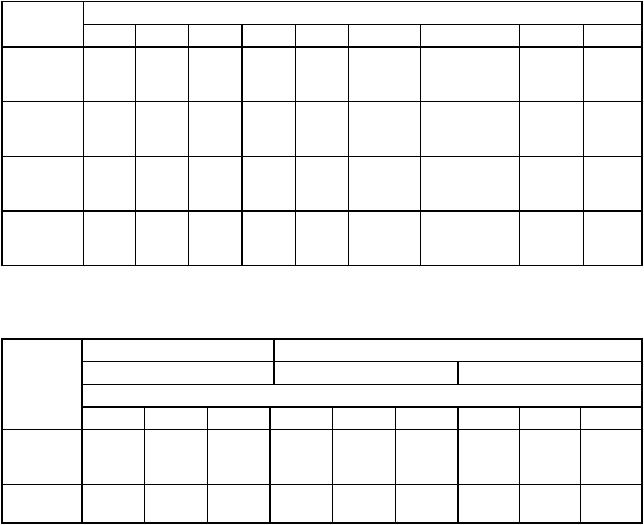
Table 9-2. Move Byte and Word Instruction Execution Times
|
|
|
|
|
Destination |
|
|
|
|
Source |
Dn |
An |
(An) |
(An)+ |
–(An) |
(d16, An) |
(d8, An, Xn)* |
(xxx).W |
(xxx).L |
Dn |
4(1/0) |
4(1/0) |
8(1/1) |
8(1/1) |
8(1/1) |
12(2/1) |
14(2/1) |
12(2/1) |
16(3/1) |
An |
4(1/0) |
4(1/0) |
8(1/1) |
8(1/1) |
8(1/1) |
12(2/1) |
14(2/1) |
12(2/1) |
16(3/1) |
(An) |
8(2/0) |
8(2/0) |
12(2/1) |
12(2/1) |
12(2/1) |
16(3/1) |
18(3/1) |
16(3/1) |
20(4/1) |
(An)+ |
8(2/0) |
8(2/0) |
12(2/1) |
12(2/1) |
12(2/1) |
16(3/1) |
18(3/1) |
16(3/1) |
20(4/1) |
–(An) |
10(2/0) |
10(2/0) |
14(2/1) |
14(2/1) |
14(2/1) |
18(3/1) |
20(3/1) |
18(3/1) |
22(4/1) |
(d 16, An) |
12(3/0) |
12(3/0) |
16(3/1) |
16(3/1) |
16(3/1) |
20(4/1) |
22(4/1) |
20(4/1) |
24(5/1) |
(d 8, An, Xn)* |
14(3/0) |
14(3/0) |
18(3/1) |
18(3/1) |
18(3/1) |
22(4/1) |
24(4/1) |
22(4/1) |
26(5/1) |
(xxx).W |
12(3/0) |
12(3/0) |
16(3/1) |
16(3/1) |
16(3/1) |
20(4/1) |
22(4/1) |
20(4/1) |
24(5/1) |
(xxx).L |
16(4/0) |
16(4/0) |
20(4/1) |
20(4/1) |
20(4/1) |
24(5/1) |
26(5/1) |
24(5/1) |
28(6/1) |
(d 16, PC) |
12(3/0) |
12(3/0) |
16(3/1) |
16(3/1) |
16(3/1) |
20(4/1) |
22(4/1) |
20(4/1) |
24(5/1) |
(d 8, PC, Xn)* |
14(3/0) |
14(3/0) |
18(3/1) |
18(3/1) |
18(3/1) |
22(4/1) |
24(4/1) |
22(4/1) |
26(5/1) |
#<data> |
8(2/0) |
8(2/0) |
12(2/1) |
12(2/1) |
12(2/1) |
16(3/1) |
18(3/1) |
16(3/1) |
20(4/1) |
*The size of the index register (Xn) does not affect execution time.
Table 9-3. Move Byte and Word Instruction Loop Mode Execution Times
|
|
Loop Continued |
|
|
Loop Terminated |
|
|
||
|
Valid Count, cc False |
Valid count, cc True |
|
Expired Count |
|
||||
|
|
|
|
|
Destination |
|
|
|
|
Source |
(An) |
(An)+ |
–(An) |
(An) |
(An)+ |
–(An) |
(An) |
(An)+ |
–(An) |
Dn |
10(0/1) |
10(0/1) |
— |
18(2/1) |
18(2/1) |
— |
16(2/1) |
16(2/1) |
— |
An* |
10(0/1) |
10(0/1) |
— |
18(2/1) |
18(2/1) |
— |
16(2/1) |
16(2/1) |
— |
(An) |
14(1/1) |
14(1/1) |
16(1/1) |
20(3/1) |
20(3/1) |
22(3/1) |
18(3/1) |
18(3/1) |
20(3/1) |
(An)+ |
14(1/1) |
14(1/1) |
16(1/1) |
20(3/1) |
20(3/1) |
22(3/1) |
18(3/1) |
18(3/1) |
20(3/1) |
–(An) |
16(1/1) |
16(1/1) |
18(1/1) |
22(3/1) |
22(3/1) |
24(3/1) |
20(3/1) |
20(3/1) |
22(3/1) |
*Word only.
MOTOROLA |
M68000 8-/16-/32-BIT MICROPROCESSORS USER’S MANUAL |
9-3 |
Table 9-4. Move Long Instruction Execution Times
|
|
|
|
|
Destination |
|
|
|
|
Source |
Dn |
An |
(An) |
(An)+ |
–(An) |
(d16, An) |
(d8, An, Xn)* |
(xxx).W |
(xxx).L |
Dn |
4(1/0) |
4(1/0) |
12(1/2) |
12(1/2) |
14(1/2) |
16(2/2) |
18(2/2) |
16(2/2) |
20(3/2) |
An |
4(1/0) |
4(1/0) |
12(1/2) |
12(1/2) |
14(1/2) |
16(2/2) |
18(2/2) |
16(2/2) |
20(3/2) |
(An) |
12(3/0) |
12(3/0) |
20(3/2) |
20(3/2) |
20(3/2) |
24(4/2) |
26(4/2) |
24(4/2) |
28(5/2) |
(An)+ |
12(3/0) |
12(3/0) |
20(3/2) |
20(3/2) |
20(3/2) |
24(4/2) |
26(4/2) |
24(4/2) |
28(5/2) |
–(An) |
14(3/0) |
14(3/0) |
22(3/2) |
22(3/2) |
22(3/2) |
26(4/2) |
28(4/2) |
26(4/2) |
30(5/2) |
(d 16, An) |
16(4/0) |
16(4/0) |
24(4/2) |
24(4/2) |
24(4/2) |
28(5/2) |
30(5/2) |
28(5/2) |
32(6/2) |
(d 8, An, Xn)* |
18(4/0) |
18(4/0) |
26(4/2) |
26(4/2) |
26(4/2) |
30(5/2) |
32(5/2) |
30(5/2) |
34(6/2) |
(xxx).W |
16(4/0) |
16(4/0) |
24(4/2) |
24(4/2) |
24(4/2) |
28(5/2) |
30(5/2) |
28(5/2) |
32(6/2) |
(xxx).L |
20(5/0) |
20(5/0) |
28(5/2) |
28(5/2) |
28(5/2) |
32(6/2) |
34(6/2) |
32(6/2) |
36(7/2) |
(d 16, PC) |
16(4/0) |
16(4/0) |
24(4/2) |
24(4/2) |
24(4/2) |
28(5/2) |
30(5/2) |
28(5/2) |
32(5/2) |
(d 8, PC, Xn)* |
18(4/0) |
18(4/0) |
26(4/2) |
26(4/2) |
26(4/2) |
30(5/2) |
32(5/2) |
30(5/2) |
34(6/2) |
#<data> |
12(3/0) |
12(3/0) |
20(3/2) |
20(3/2) |
20(3/2) |
24(4/2) |
26(4/2) |
24(4/2) |
28(5/2) |
*The size of the index register (Xn) does not affect execution time.
Table 9-5. Move Long Instruction Loop Mode Execution Times
|
|
Loop Continued |
|
|
Loop Terminated |
|
|
||
|
Valid Count, cc False |
Valid count, cc True |
|
Expired Count |
|
||||
|
|
|
|
|
Destination |
|
|
|
|
Source |
(An) |
(An)+ |
–(An) |
(An) |
(An)+ |
–(An) |
(An) |
(An)+ |
–(An) |
Dn |
14(0/2) |
14(0/2) |
— |
20(2/2) |
20(2/2) |
— |
18(2/2) |
18(2/2) |
— |
An |
14(0/2) |
14(0/2) |
— |
20(2/2) |
20(2/2) |
— |
18(2/2) |
18(2/2) |
— |
(An) |
22(2/2) |
22(2/2) |
24(2/2) |
28(4/2) |
28(4/2) |
30(4/2) |
24(4/2) |
24(4/2) |
26(4/2) |
(An)+ |
22(2/2) |
22(2/2) |
24(2/2) |
28(4/2) |
28(4/2) |
30(4/2) |
24(4/2) |
24(4/2) |
26(4/2) |
–(An) |
24(2/2) |
24(2/2) |
26(2/2) |
30(4/2) |
30(4/2) |
32(4/2) |
26(4/2) |
26(4/2) |
28(4/2) |
9.3 STANDARD INSTRUCTION EXECUTION TIMES
The numbers of clock periods shown in tables 9-6 and 9-7 indicate the times required to perform the operations, store the results, and read the next instruction. The total number of clock periods, the number of read cycles, and the number of write cycles are shown in the previously described format. The number of clock periods, the number of read cycles, and the number of write cycles, respectively, must be added to those of the effective address calculation where indicated by a plus sign (+).
In Tables 9-6 and 9-7, the following notation applies:
An — Address register operand Sn — Data register operand
ea — An operand specified by an effective address
M — Memory effective address operand
9-4 |
M68000 8-/16-/32-BIT MICROPROCESSORS USER'S MANUAL |
MOTOROLA |
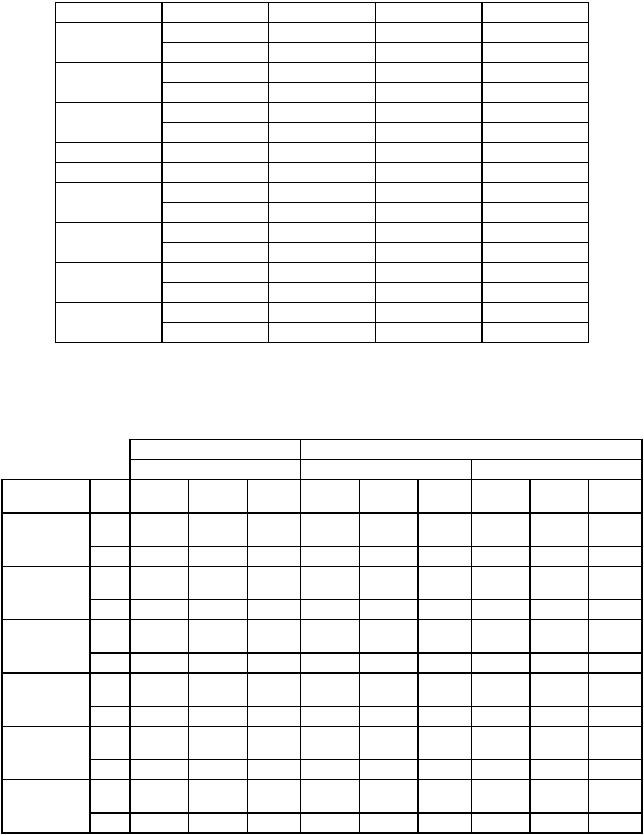
Table 9-6. Standard Instruction Execution Times
Instruction |
Size |
op<ea>, An*** |
op<ea>, Dn |
op Dn, <M> |
ADD/ADDA |
Byte, Word |
8(1/0)+ |
4(1/0)+ |
8(1/1)+ |
|
Long |
6(1/0)+ |
6(1/0)+ |
12(1/2)+ |
AND |
Byte, Word |
— |
4(1/0)+ |
8(1/1)+ |
|
Long |
— |
6(1/0)+ |
12(1/2)+ |
CMP/CMPA |
Byte, Word |
6(1/0)+ |
4(1/0)+ |
— |
|
Long |
6(1/0)+ |
6(1/0)+ |
— |
DIVS |
— |
— |
122(1/0)+ |
— |
DIVU |
— |
— |
108(1/0)+ |
— |
EOR |
Byte, Word |
— |
4(1/0)** |
8(1/1)+ |
|
Long |
— |
6(1/0)** |
12(1/2)+ |
MULS/MULU |
— |
— |
42(1/0)+* |
— |
|
— |
— |
40(1/0)* |
— |
OR |
Byte, Word |
— |
4(1/0)+ |
8(1/1)+ |
|
Long |
— |
6(1/0)+ |
12(1/2)+ |
SUB/SUBA |
Byte, Word |
8(1/0)+ |
4(1/0)+ |
8(1/1)+ |
|
Long |
6(1/0)+ |
6(1/0)+ |
12(1/2)+ |
+ Add effective address calculation time.
*Indicates maximum value.
**Only available address mode is data register direct.
***Word or long word only.
Table 9-7 Standard Instruction Loop Mode Execution Times
|
|
Loop Continued |
|
|
Loop Terminated |
|
|
|||
|
|
Valid Count cc False |
Valid Count cc True |
Expired Count |
||||||
|
|
op<ea>, |
op<ea>, |
op Dn, |
op<ea>, |
op<ea>, |
op Dn, |
op<ea>, |
op<ea>, |
op Dn, |
Instruction |
Size |
An* |
Dn |
<ea> |
An* |
Dn |
<ea> |
An* |
Dn |
<ea> |
ADD |
Byte, |
18(1/0) |
16(1/0) |
16(1/1) |
24(3/0) |
22(3/0) |
22(3/1) |
22(3/0) |
20(3/0) |
20(3/1) |
|
Word |
|
|
|
|
|
|
|
|
|
|
Long |
22(2/0) |
22(2/0) |
24(2/2) |
28(4/0) |
28(4/0) |
30(4/2) |
26(4/0) |
26(4/0) |
28(4/2) |
AND |
Byte, |
— |
16(1/0) |
16(1/1) |
— |
22(3/0) |
22(3/1) |
— |
20(3/0) |
20(3/1) |
|
Word |
|
|
|
|
|
|
|
|
|
|
Long |
— |
22(2/0) |
24(2/2) |
— |
28(4/0) |
30(4/2) |
— |
26(4/0) |
28(4/2) |
CMP |
Byte, |
12(1/0) |
12(1/0) |
— |
18(3/0) |
18(3/0) |
— |
16(3/0) |
16(4/0) |
— |
|
Word |
|
|
|
|
|
|
|
|
|
|
Long |
18(2/0) |
18(2/0) |
— |
24(4/0) |
24(4/0) |
— |
20(4/0) |
20(4/0) |
— |
EOR |
Byte, |
— |
— |
16(1/0) |
— |
— |
22(3/1) |
— |
— |
20(3/1) |
|
Word |
|
|
|
|
|
|
|
|
|
|
Long |
— |
— |
24(2/2) |
— |
— |
30(4/2) |
— |
— |
28(4/2) |
OR |
Byte, |
— |
16(1/0) |
16(1/0) |
— |
22(3/0) |
22(3/1) |
— |
20(3/0) |
20(3/1) |
|
Word |
|
|
|
|
|
|
|
|
|
|
Long |
— |
22(2/0) |
24(2/2) |
— |
28(4/0) |
30(4/2) |
— |
26(4/0) |
28(4/2) |
SUB |
Byte, |
18(1/0) |
16(1/0) |
16(1/1) |
24(3/0) |
22(3/0) |
22(3/1) |
22(3/0) |
20(3/0) |
20(3/1) |
|
Word |
|
|
|
|
|
|
|
|
|
|
Long |
22(2/0) |
20(2/0) |
24(2/2) |
28(4/0) |
26(4/0) |
30(4/2) |
26(4/0) |
24(4/0) |
28(4/2) |
*Word or long word only.
<ea> may be (An), (An)+, or –(An) only. Add two clock periods to the table value if <ea> is –(An).
MOTOROLA |
M68000 8-/16-/32-BIT MICROPROCESSORS USER’S MANUAL |
9-5 |