

A double bus fault occurs during a reset operation when a bus error occurs while the processor is reading the vector table (before the first instruction is executed). The reset operation is described in the following paragraph.
5.5 RESET OPERATION
RESET is asserted externally for the initial processor reset. Subsequently, the signal can be asserted either externally or internally (executing a RESET instruction). For proper external reset operation, HALT must also be asserted.
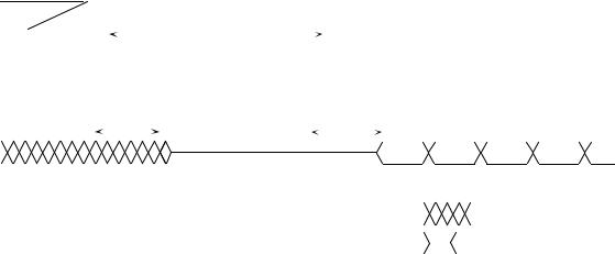
When RESET and HALT are driven by an external device, the entire system, including the processor, is reset. Resetting the processor initializes the internal state. The processor reads the reset vector table entry (address $00000) and loads the contents into the supervisor stack pointer (SSP). Next, the processor loads the contents of address $00004 (vector table entry 1) into the program counter. Then the processor initializes the interrupt level in the status register to a value of seven. In the MC68010, the processor also clears the vector base register to $00000. No other register is affected by the reset sequence. Figure 5-30 shows the timing of the reset operation.
CLK |
|
|
|
|
|
|
|
|
|
|
|
|
|
|
|
|
|
|
|
|
|
|
|
|
|
|
|
|
|
|
|
|
|
|
|
|
|
|
|
|
|
|
|
|
|
|
|
|
|
|
|
|
|
|
|
|
|
|
|
|
|
|
|
|
|
|
|
|
|
|
|
|
|
|
|
|
|
|
|
|
|
|
|
|
|
|
|
|
|
|
|
|
|||
|
|
|
|
|
|
|
|
|
|
|
|
|
|
|
|
|
|
|
|
|
|
|
|
|
|
|
|
|
|
|
|
|
|
|
|
|
|
|
|
|
|
|
|
|
|
|
|
|
|
|
|
|
|
|
|
|
|
|
|
|
|
|
|
|
|
|
|
|
|
|
|
|
|
|
|
|
|
|
|
|
|
|
|
|
|
|
|
|
|
|
|
|
|
|
|
+ 5 VOLTS |
|
|
|
|
|
|
|
|
|
|
|
|
|
|
|
|
|
|
|
|
|
|
|
|
|
|
|
|
|
|
|
|
|
|
|
|
|
|
|
|
|
|
|
|
|
|
|
|
|
|
|
|
|
|
|
|
|
|
|
|
|
|
|
|
|
|
|
|
|
|
|
|
|
|
|
|
|
|
|
|
|
|
|
|
|
|
|
|
|
|
|
|
|||
|
|
|
|
|
|
|
|
|
|
|
|
|
|
|
|
|
|
|
|
|
|
|
|
|
|
|
|
|
|
|
|
|
|
|
|
|
|
|
|
|
|
|
|
|
|
|
|
|
|
|
|
|
|
|
|
|
|
|
|
|
|
|
|
|
|
|
|
|
|
|
|
|
|
|
|
|
|
|
|
|
|
|
|
|
|
|
|
|
|
|
|
||||
VCC |
|
|
|
|
|
|
|
|
|
|
|
|
|
|
|
|
|
|
|
|
|
|
|
|
|
|
|
|
|
|
|
|
|
|
|
|
|
|
|
|
|
|
|
|
|
|
|
|
|
|
|
|
|
|
|
|
|
|
|
|
|
|
|
|
|
|
|
|
|
|
|
|
|
|
|
|
|
|
|
|
|
|
|
|
|
|
|
|
|
|
|
|
|
|
|
|
|
|
|
|
|
|
|
|
|
|
|
|
|
|
|
|
|
|
|
|
|
|
|
|
|
T |
³ 100 MILLISECONDS |
|
|
|
|
|
|
|
|
|
|
|
|
|
|
|
|
|
|
|
|
|
|
|
|
|
|
|
|
|
|
|
|
|
|
|
|
|
|
|
|
|
|
|
|
|
|
|
|
|
|
|
|
||||||||||||||||
RESET |
|
|
|
|
|
|
|
|
|
|
|
|
|
|
|
|
|
|
|
|
|
|
|
|
|
|
|
|
|
|
|
|
|
|
|
|
|
|
|
|
|
|
|
|
|
|
|
|
|
|
|
|
|
|
|
|
|
|
|
|
|
|
|
|
|
|
|
|
|
|
|
|
|
|
|
|
|||||||||||||||||||
|
|
|
|
|
|
|
|
|
|
|
|
|
|
|
|
|
|
|
|
|
|
|
|
|
|
|
|
|
|
|
|
|
|
|
|
|
|
|
|
|
|
|
|
|
|
|
|
|
|
|
|
|
|
|
|
|
|
|
|
|
|
|
|
|
|
|
|
|
|
|
|
|
|
|
|
|
|
|
|
|
|
|
|
|
|
|
|
|
|
|
|
||||
HALT |
|
|
|
|
|
|
|
|
|
|
|
|
|
|
|
|
|
|
|
|
|
|
|
|
|
|
|
|
|
|
|
|
|
|
|
|
|
|
|
|
|
|
|
|
|
|
|
|
|
|
|
|
|
|
|
|
|
|
|
|
|
|
|
|
|
|
|
|
|
|
|
|
|
|
|
|
|
|
|
|
|
|
|
|
|
|
|
|
|
|
|
|
|||
|
|
|
|
|
|
|
|
|
|
|
|
|
|
|
|
|
|
|
|
|
|
|
|
|
|
|
|
|
|
|
|
|
|
|
|
|
|
|
|
|
|
|
|
|
|
|
|
|
|
|
|
|
|
|
|
|
|
|
|
|
|
|
|
|
|
|
|
|
|
|
|
|
|
|
|
|
|
|
|
|
|
|
|
|
|
|
|
|
|
|
|
||||
|
|
|
|
|
|
|
|
|
|
|
|
|
|
|
|
|
|
|
|
|
|
|
|
|
|
|
|
|
|
|
|
|
|
|
|
|
|
|
|
|
|
|
|
|
|
|
|
|
|
|
|
|
|
|
|
|
|
|
|
|
|
|
|
|
|
|
|
|
|
|
|
|
|
|
|
|
|
|
|
|
|
|
|
|
|
|
|
|
|
|
|
||||
|
|
|
|
|
|
|
|
|
|
|
|
|
|
|
|
|
|
|
|
|
|
|
|
|
|
|
|
|
|
|
|
|
|
|
|
|
|
|
|
|
|
|
|
|
|
|
|
|
|
|
|
|
|
|
|
|
|
|
|
|
|
|
|
|
|
|
|
|
|
|
|
|
|
|
|
|
|||||||||||||||||||
|
|
|
|
|
|
|
|
|
|
|
|
|
|
|
|
|
|
|
|
|
|
|
|
|
|
|
|
|
|
T < 4 CLOCKS |
|
|
|
|
|
|
|
|
|
|
|
|
|
|
|
|
|
|
|
|
|
|
|
|
|
|
|
|
|
|
|
|
|
|
|
|
|
|
|
|
|
|
|
|
|
||||||||||||||||||||
|
|
|
|
|
|
|
|
|
|
|
|
|
|
|
|
|
|
|
|
|
|
|
|
|
|
|
|
|
|
|
|
|
1 |
|
|
|
|
|
|
|
|
|
|
|
|
|
|
|
|
|
|
|
|
|
|
|
|
|
|
|
|
|
|
|
|
|
|
|
|
|
|
|
|
|
|||||||||||||||||||||
|
|
|
|
|
|
|
|
|
|
|
|
|
|
|
|
|
|
|
|
|
|
|
|
|
|
|
|
|
|
|
|
|
|
|
|
|
|
|
|
|
|
|
|
|
|
|
|
|
|
|
|
|
|
|
|
|
|
|
|
|
|
|
|
|
|
|
|
|
|
|
|
||||||||||||||||||||||||
|
|
|
|
|
|
|
|
|
|
|
|
|
|
|
|
|
|
|
|
|
|
|
|
|
|
|
|
|
|
|
|
|
|
|
|
|
|
|
|
|
|
|
|
|
|
|
|
|
|
|
|
|
|
|
|
|
|
|
|
|
|
|
|
|
|
|
|
|
|
|
|
|
|
|
|
|
|
|
|
|
|
|
|
|
|
|
|
|
|
|
|
|
|
|
|
BUS CYCLES
|
|
|
|
2 |
3 |
4 |
5 |
6 |
|
NOTES: |
|
|
|
|
|
|
|
|
|
1. |
Internal start-up time |
4. |
PC High read in here |
Bus State Unknown: |
|
|
|
|
|
2. |
SSP high read in here |
5. |
PC Low read in here |
|
|
|
|
|
|
3. |
SSP low read in here |
6. |
First instruction fetched here |
All Control Signals Inactive. |
|
|
|
|
|
|
|
|
|
|
|
|
|||
|
|
|
|
Data Bus in Read Mode: |
|
|
|
|
|
Figure 5-30. Reset Operation Timing Diagram
The RESET instruction causes the processor to assert RESET for 124 clock periods to reset the external devices of the system. The internal state of the processor is not affected. Neither the status register nor any of the internal registers is affected by an internal reset operation. All external devices in the system should be reset at the completion of the RESET instruction.
For the initial reset, RESET and HALT must be asserted for at least 100 ms. For a subsequent external reset, asserting these signals for 10 clock cycles or longer resets the processor. However, an external reset signal that is asserted while the processor is
MOTOROLA |
M68000 8-/16-/32-BIT MICROPROCESSORS USER'S MANUAL |
5-29 |
executing a reset instruction is ignored. Since the processor asserts the RESET signal for
124 clock cycles during execution of a reset instruction, an external reset should assert
RESET for at least 132 clock periods.
5.6 THE RELATIONSHIP OF |
, |
, AND |
To properly control termination of a bus cycle for a retry or a bus error condition, DTACK,
BERR, and HALT should be asserted and negated on the rising edge of the processor clock. This relationship assures that when two signals are asserted simultaneously, the required setup time (specification #47, Section 9 Electrical Characteristics) for both of them is met during the same bus state. External circuitry should be designed to incorporate this precaution. A related specification, #48, can be ignored when DTACK,
BERR, and HALT are asserted and negated on the rising edge of the processor clock.
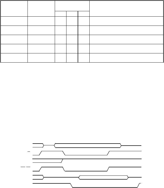
The possible bus cycle termination can be summarized as follows (case numbers refer to Table 5-5).
Normal Termination: DTACK is asserted. BERR and HALT remain negated (case 1).
Halt Termination: HALT is asserted coincident with or preceding DTACK, and BERR remains negated (case 2).
Bus Error Termination: BERR is asserted in lieu of, coincident with, or preceding
DTACK (case 3). In the MC68010, the late bus error also, BERR is asserted following DTACK (case 4). HALT remains negated and BERR is negated coincident with or after DTACK.
Retry Termination: HALT and BERR asserted in lieu of, coincident with, or before DTACK (case 5). In the MC68010, the late retry also, BERR and HALT are asserted following DTACK (case 6). BERR is negated coincident with or after DTACK. HALT must be held at least one cycle after BERR.
Table 5-1 shows the details of the resulting bus cycle termination in the M68000 microprocessors for various combinations of signal sequences.
5-30 |
M68000 8-/16-/32-BIT MICROPROCESSORS USER'S MANUAL |
MOTOROLA |

|
|
Table 5-1. |
, |
, and |
Assertion Results |
||
|
|
Asserted on |
|
|
|
|
|
Case |
Control |
Rising Edge |
MC68000/MC68HC000/001 |
|
MC68010 Results |
||
No. |
Signal |
of State |
EC000/MC68008 Results |
|
|
||
|
|
N |
N+2 |
|
|
|
|
1 |
DTACK |
A |
S |
Normal cycle terminate and continue. |
Normal cycle terminate and continue. |
||
|
BERR |
NA |
NA |
|
|
|
|
|
HALT |
NA |
X |
|
|
|
|
2 |
DTACK |
A |
S |
Normal cycle terminate and halt. |
|
Normal cycle terminate and halt. |
|
|
BERR |
NA |
NA |
Continue when HALT negated. |
|
Continue when HALT negated. |
|
|
HALT |
A/S |
S |
|
|
|
|
3 |
DTACK |
X |
X |
Terminate and take bus error trap. |
Terminate and take bus error trap. |
||
|
BERR |
A |
S |
|
|
|
|
|
HALT |
NA |
NA |
|
|
|
|
4 |
DTACK |
A |
S |
Normal cycle terminate and continue. |
Terminate and take bus error trap. |
||
|
BERR |
NA |
A |
|
|
|
|
|
HALT |
NA |
NA |
|
|
|
|
5 |
DTACK |
X |
X |
Terminate and retry when HALT |
|
Terminate and retry when HALT |
|
|
BERR |
A |
S |
removed. |
|
|
removed. |
|
HALT |
A/S |
S |
|
|
|
|
6 |
DTACK |
A |
S |
Normal cycle terminate and continue. |
Terminate and retry when HALT |
||
|
BERR |
NA |
A |
|
|
|
removed. |
|
HALT |
NA |
A |
|
|
|
|
LEGEND:
N — The number of the current even bus state (e.g., S4, S6, etc.)
A — Signal asserted in this bus state
NA — Signal not asserted in this bus state
X — Don't care
S — Signal asserted in preceding bus state and remains asserted in this state
NOTE: All operations are subject to relevant setup and hold times.
The negation of BERR and HALT under several conditions is shown in Table 5-6. (DTACK is assumed to be negated normally in all cases; for reliable operation, both DTACK and BERR should be negated when address strobe is negated).
EXAMPLE A:
A system uses a watchdog timer to terminate accesses to unused address space. The timer asserts BERR after timeout (case 3).
EXAMPLE B:
A system uses error detection on random-access memory (RAM) contents. The system designer may:
1.Delay DTACK until the data is verified. If data is invalid, return BERR and HALT simultaneously to retry the error cycle (case 5).
2.Delay DTACK until the data is verified. If data is invalid, return BERR at the same time as DTACK (case 3).
3.For an MC68010, return DTACK before data verification. If data is invalid, assert BERR and HALT to retry the error cycle (case 6).
MOTOROLA |
M68000 8-/16-/32-BIT MICROPROCESSORS USER'S MANUAL |
5-31 |
4.For an MC68010, return DTACK before data verification. If data is invalid, assert BERR on the next clock cycle (case 4).
|
Table 5-6. |
|
and |
|
Negation Results |
Conditions of |
|
Negated on Rising |
|
||
|
|
Edge of State |
|
||
Termination in |
|
|
|
||
|
|
|
|
|
|
Table 4-4 |
Control Signal |
N |
|
N+2 |
Results—Next Cycle |
Bus Error |
BERR |
• |
or |
• |
Takes bus error trap. |
|
HALT |
• |
or |
• |
|
Rerun |
BERR |
• |
or |
• |
Illegal sequence; usually traps to vector number 0. |
|
HALT |
• |
|
|
|
Rerun |
BERR |
• |
|
|
Reruns the bus cycle. |
|
HALT |
|
|
• |
|
Normal |
BERR |
• |
|
|
May lengthen next cycle. |
|
HALT |
• |
or |
• |
|
Normal |
BERR |
|
|
• |
If next cycle is started, it will be terminated as a bus |
|
HALT |
• |
or |
none |
error. |
• = Signal is negated in this bus state.
5.7 ASYNCHRONOUS OPERATION
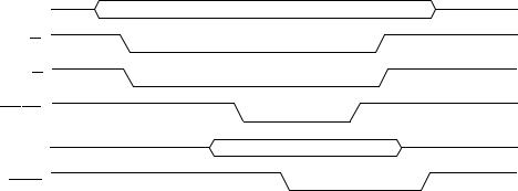
To achieve clock frequency independence at a system level, the bus can be operated in an asynchronous manner. Asynchronous bus operation uses the bus handshake signals to control the transfer of data. The handshake signals are AS, UDS, LDS, DS (MC68008 only), DTACK, BERR, HALT, AVEC (MC68EC000 only), and VPA (only for M6800 peripheral cycles). AS indicates the start of the bus cycle, and UDS, LDS, and DS signal valid data for a write cycle. After placing the requested data on the data bus (read cycle) or latching the data (write cycle), the slave device (memory or peripheral) asserts DTACK to terminate the bus cycle. If no device responds or if the access is invalid, external control logic asserts BERR, or BERR and HALT, to abort or retry the cycle. Figure 5-31 shows the use of the bus handshake signals in a fully asynchronous read cycle. Figure 5-32 shows a fully asynchronous write cycle.
ADDR
AS
R/W
UDS/LDS
DATA
DTACK
Figure 5-31. Fully Asynchronous Read Cycle
5-32 |
M68000 8-/16-/32-BIT MICROPROCESSORS USER'S MANUAL |
MOTOROLA |
ADDR
AS
R/W
UDS/LDS
DATA
DTACK
Figure 5-32. Fully Asynchronous Write Cycle
In the asynchronous mode, the accessed device operates independently of the frequency and phase of the system clock. For example, the MC68681 dual universal asynchronous receiver/transmitter (DUART) does not require any clock-related information from the bus master during a bus transfer. Asynchronous devices are designed to operate correctly with processors at any clock frequency when relevant timing requirements are observed.
A device can use a clock at the same frequency as the system clock (e.g., 8, 10, or 12.5, 16, and 20MHz), but without a defined phase relationship to the system clock. This mode of operation is pseudo-asynchronous; it increases performance by observing timing parameters related to the system clock frequency without being completely synchronous with that clock. A memory array designed to operate with a particular frequency processor but not driven by the processor clock is a common example of a pseudo-asynchronous device.
The designer of a fully asynchronous system can make no assumptions about address setup time, which could be used to improve performance. With the system clock frequency known, the slave device can be designed to decode the address bus before recognizing an address strobe. Parameter #11 (refer to Section 10 Electrical Characteristics) specifies the minimum time before address strobe during which the address is valid.
In a pseudo-asynchronous system, timing specifications allow DTACK to be asserted for a read cycle before the data from a slave device is valid. The length of time that DTACK may precede data is specified as parameter #31. This parameter must be met to ensure the validity of the data latched into the processor. No maximum time is specified from the assertion of AS to the assertion of DTACK. During this unlimited time, the processor inserts wait cycles in one-clock-period increments until DTACK is recognized. Figure 5-33 shows the important timing parameters for a pseudo-asynchronous read cycle.
MOTOROLA |
M68000 8-/16-/32-BIT MICROPROCESSORS USER'S MANUAL |
5-33 |
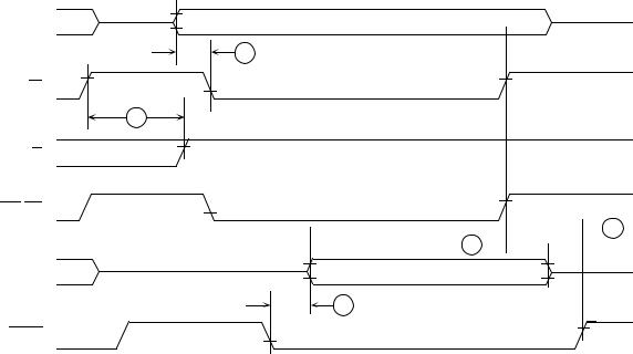
ADDR
11
AS
17
R/W
UDS/LDS

 28 29
28 29 

DATA
31
DTACK
Figure 5-33. Pseudo-Asynchronous Read Cycle
During a write cycle, after the processor asserts AS but before driving the data bus, the processor drives R/W low. Parameter #55 specifies the minimum time between the transition of R/W and the driving of the data bus, which is effectively the maximum turnoff time for any device driving the data bus.
After the processor places valid data on the bus, it asserts the data strobe signal(s). A data setup time, similar to the address setup time previously discussed, can be used to improve performance. Parameter #29 is the minimum time a slave device can accept valid data before recognizing a data strobe. The slave device asserts DTACK after it accepts the data. Parameter #25 is the minimum time after negation of the strobes during which the valid data remains on the address bus. Parameter #28 is the maximum time between the negation of the strobes by the processor and the negation of DTACK by the slave device. If DTACK remains asserted past the time specified by parameter #28, the processor may recognize it as being asserted early in the next bus cycle and may terminate that cycle prematurely. Figure 5-34 shows the important timing specifications for a pseudo-asynchronous write cycle.
5-34 |
M68000 8-/16-/32-BIT MICROPROCESSORS USER'S MANUAL |
MOTOROLA |