

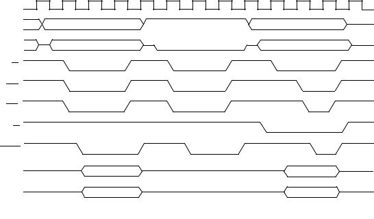
The breakpoint acknowledge cycle is performed by the MC68010 to provide an indication to hardware that a software breakpoint is being executed when the processor executes a breakpoint (BKPT) instruction. The processor neither accepts nor sends data during this cycle, which is otherwise similar to a read cycle. The cycle is terminated by either DTACK,
BERR, or as an M6800 peripheral cycle when VPA is asserted, and the processor continues illegal instruction exception processing. Figure 5-12 illustrates the timing diagram for the breakpoint acknowledge cycle.
S0 |
S2 |
S4 |
S6 |
S0 |
S2 |
S4 |
S6 |
S0 |
S2 |
S4 |
S6 |
CLK
FC2–FC0
A23–A1
AS
UDS
LDS
R/W
DTACK
D15–D8
D7–D0
 WORD READ
 BREAKPOINT
 STACK PC LOW

CYCLE
Figure 5-12. Breakpoint Acknowledge Cycle Timing Diagram
5.2 BUS ARBITRATION
Bus arbitration is a technique used by bus master devices to request, to be granted, and to acknowledge bus mastership. Bus arbitration consists of the following:
1.Asserting a bus mastership request
2.Receiving a grant indicating that the bus is available at the end of the current cycle
3.Acknowledging that mastership has been assumed
There are two ways to arbitrate the bus, 3-wire and 2-wire bus arbitration. The MC68000,
MC68HC000, MC68EC000, MC68HC001, MC68008, and MC68010 can do 2-wire bus arbitration. The MC68000, MC68HC000, MC68HC001, and MC68010 can do 3-wire bus arbitration. Figures 5-13 and 5-15 show 3-wire bus arbitration and Figures 5-14 and 5-16 show 2-wire bus arbitration. Bus arbitration on all microprocessors, except the 48-pin MC68008 and MC68EC000, BGACK must be pulled high for 2-wire bus arbitration.
MOTOROLA |
M68000 8-/16-/32-BIT MICROPROCESSORS USER'S MANUAL |
5-11 |
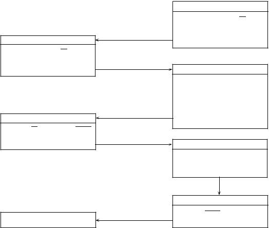
PROCESSOR
GRANT BUS ARBITRATION
1) ASSERT BUS GRANT (BG)
TERMINATE ARBITRATION
1)NEGATE BG (AND WAIT FOR BGACK TO BE NEGATED)
REARBITRATE OR RESUME
PROCESSOR OPERATION
REQUESTING DEVICE
REQUEST THE BUS
1) ASSERT BUS REQUEST (BR)
ACKNOWLEDGE BUS MASTERSHIP
1)EXTERNAL ARBITRATION DETERMINES NEXT BUS MASTER
2)NEXT BUS MASTER WAITS FOR CURRENT CYCLE TO COMPLETE
3)NEXT BUS MASTER ASSERTS BUS GRANT ACKNOWLEDGE (BGACK) TO BECOME NEW MASTER
4)BUS MASTER NEGATES BR
OPERATE AS BUS MASTER
1)PERFORM DATA TRANSFERS (READ
AND WRITE CYCLES) ACCORDING TO THE SAME RULES THE PROCESSOR USES
RELEASE BUS MASTERSHIP
1) NEGATE BGACK
Figure 5-13. 3-Wire Bus Arbitration Cycle Flowchart (Not Applicable to 48-Pin MC68008 or MC68EC000)
5-12 |
M68000 8-/16-/32-BIT MICROPROCESSORS USER'S MANUAL |
MOTOROLA |
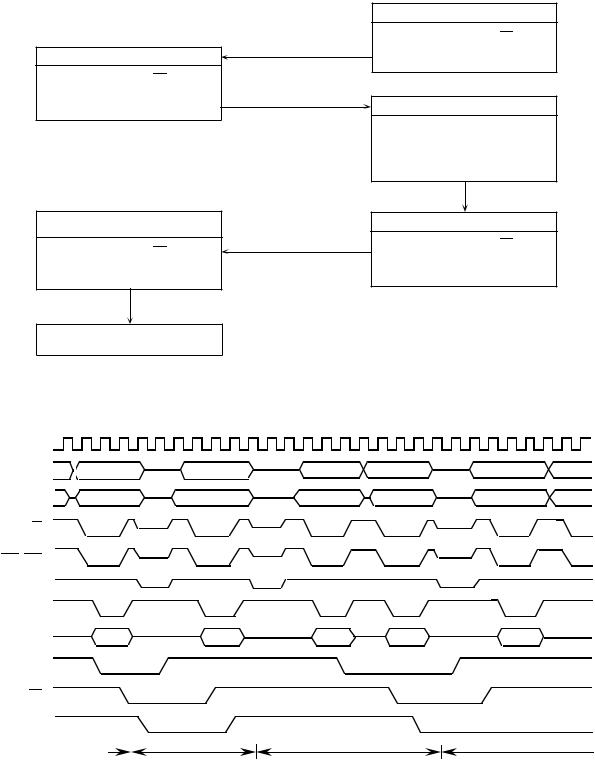
PROCESSOR
GRANT BUS ARBITRATION
1) ASSERT BUS GRANT (BG)
ACKNOWLEDGE RELEASE OF
BUS MASTERSHIP
1) NEGATE BUS GRANT (BG)
REARBITRATE OR RESUME PROCESSOR OPERATION
REQUESTING DEVICE
REQUEST THE BUS
1) ASSERT BUS REQUEST (BR)
OPERATE AS BUS MASTER
1)EXTERNAL ARBITRATION DETERMINES NEXT BUS MASTER
2)NEXT BUS MASTER WAITS FOR CURRENT CYCLE TO COMPLETE
RELEASE BUS MASTERSHIP
1) NEGATE BUS REQUEST (BR)
Figure 5-14. 2-Wire Bus Arbitration Cycle Flowchart
CLK
FC2–FC0
A23–A1
AS
LDS/ UDS
R/W
DTACK
D15–D0
BR
BG
BGACK
PROCESSOR |
|
DMA DEVICE |
|
PROCESSOR |
|
DMA DEVICE |
Figure 5-15. 3-Wire Bus Arbitration Timing Diagram (Not Applicable to 48-Pin MC68008 or MC68EC000)
MOTOROLA |
M68000 8-/16-/32-BIT MICROPROCESSORS USER'S MANUAL |
5-13 |

S0 |
S2 |
S4 |
S6 |
S0 |
S2 |
S4 |
S6 |
S0 |
S2 |
S4 |
S6 |
S0 |
S2 |
S4 |
S6 |
CLK
FC2–FC0
A19–A0
AS
DS
R/W
DTACK
D7–D0
BR
BG
|
|
|
|
|
|
|
|
|
|
|
|
|
|
|
|
PROCESSOR |
|
|
|
|
DMA DEVICE |
|
|
|
|
PROCESSOR |
|
|
|
|
DMA DEVICE |
|
|
|
|
|
|
|
|
|
|
|
|
||||
|
|
|
|
|
|
|
|
|
|
|
|
|
|
|
|
Figure 5-16. 2-Wire Bus Arbitration Timing Diagram
The timing diagram in Figure 5-15 shows that the bus request is negated at the time that an acknowledge is asserted. This type of operation applies to a system consisting of a processor and one other device capable of becoming bus master. In systems having several devices that can be bus masters, bus request lines from these devices can be wire-ORed at the processor, and more than one bus request signal could occur.
The bus grant signal is negated a few clock cycles after the assertion of the bus grant acknowledge signal. However, if bus requests are pending, the processor reasserts bus grant for another request a few clock cycles after bus grant (for the previous request) is negated. In response to this additional assertion of bus grant, external arbitration circuitry selects the next bus master before the current bus master has completed the bus activity.
The timing diagram in Figure 5-15 also applies to a system consisting of a processor and one other device capable of becoming bus master. Since the 48-pin version of the MC68008 and the MC68EC000 does not recognize a bus grant acknowledge signal, this processor does not negate bus grant until the current bus master has completed the bus activity.
5.2.1 Requesting The Bus
External devices capable of becoming bus masters assert BR to request the bus. This signal can be wire-ORed (not necessarily constructed from open-collector devices) from any of the devices in the system that can become bus master. The processor, which is at a lower bus priority level than the external devices, relinquishes the bus after it completes the current bus cycle.
The bus grant acknowledge signal on all the processors except the 48-pin MC68008 and
MC68EC000 helps to prevent the bus arbitration circuitry from responding to noise on the
5-14 |
M68000 8-/16-/32-BIT MICROPROCESSORS USER'S MANUAL |
MOTOROLA |