

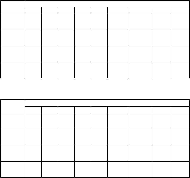
Table 7-3. Move Word Instruction Execution Times
|
|
|
|
|
Destination |
|
|
|
|
Source |
Dn |
An |
(An) |
(An)+ |
–(An) |
(d16, An) |
(d8, An, Xn)* |
(xxx).W |
(xxx).L |
Dn |
8(2/0) |
8(2/0) |
16(2/2) |
16(2/2) |
16(2/2) |
24(4/2) |
26(4/2) |
24(4/2) |
32(6/2) |
An |
8(2/0) |
8(2/0) |
16(2/2) |
16(2/2) |
16(2/2) |
24(4/2) |
26(4/2) |
24(4/2) |
32(6/2) |
(An) |
16(4/0) |
16(4/0) |
24(4/2) |
24(4/2) |
24(4/2) |
32(6/2) |
34(6/2) |
32(6/2) |
40(8/2) |
(An)+ |
16(4/0) |
16(4/0) |
24(4/2) |
24(4/2) |
24(4/2) |
32(6/2) |
34(6/2) |
32(6/2) |
40(8/2) |
–(An) |
18(4/0) |
18(4/0) |
26(4/2) |
26(4/2) |
26(4/2) |
34(6/2) |
32(6/2) |
34(6/2) |
42(8/2) |
(d 16, An) |
24(6/0) |
24(6/0) |
32(6/2) |
32(6/2) |
32(6/2) |
40(8/2) |
42(8/2) |
40(8/2) |
48(10/2) |
(d 8, An, Xn)* |
26(6/0) |
26(6/0) |
34(6/2) |
34(6/2) |
34(6/2) |
42(8/2) |
44(8/2) |
42(8/2) |
50(10/2) |
(xxx).W |
24(6/0) |
24(6/0) |
32(6/2) |
32(6/2) |
32(6/2) |
40(8/2) |
42(8/2) |
40(8/2) |
48(10/2) |
(xxx).L |
32(8/0) |
32(8/0) |
40(8/2) |
40(8/2) |
40(8/2) |
48(10/2) |
50(10/2) |
48(10/2) |
56(12/2) |
(d 16, PC) |
24(6/0) |
24(6/0) |
32(6/2) |
32(6/2) |
32(6/2) |
40(8/2) |
42(8/2) |
40(8/2) |
48(10/2) |
(d 8, PC, Xn)* |
26(6/0) |
26(6/0) |
34(6/2) |
34(6/2) |
34(6/2) |
42(8/2) |
44(8/2) |
42(8/2) |
50(10/2) |
#<data> |
16(4/0) |
16(4/0) |
24(4/2) |
24(4/2) |
24(4/2) |
32(6/2) |
34(6/2) |
32(6/2) |
40(8/2) |
*The size of the index register (Xn) does not affect execution time.
Table 7-4. Move Long Instruction Execution Times
|
|
|
|
|
Destination |
|
|
|
|
Source |
Dn |
An |
(An) |
(An)+ |
–(An) |
(d16, An) |
(d8, An, Xn)* |
(xxx).W |
(xxx).L |
Dn |
8(2/0) |
8(2/0) |
24(2/4) |
24(2/4) |
24(2/4) |
32(4/4) |
34(4/4) |
32(4/4) |
40(6/4) |
An |
8(2/0) |
8(2/0) |
24(2/4) |
24(2/4) |
24(2/4) |
32(4/4) |
34(4/4) |
32(4/4) |
40(6/4) |
(An) |
24(6/0) |
24(6/0) |
40(6/4) |
40(6/4) |
40(6/4) |
48(8/4) |
50(8/4) |
48(8/4) |
56(10/4) |
(An)+ |
24(6/0) |
24(6/0) |
40(6/4) |
40(6/4) |
40(6/4) |
48(8/4) |
50(8/4) |
48(8/4) |
56(10/4) |
–(An) |
26(6/0) |
26(6/0) |
42(6/4) |
42(6/4) |
42(6/4) |
50(8/4) |
52(8/4) |
50(8/4) |
58(10/4) |
(d 16, An) |
32(8/0) |
32(8/0) |
48(8/4) |
48(8/4) |
48(8/4) |
56(10/4) |
58(10/4) |
56(10/4) |
64(12/4) |
(d 8, An, Xn)* |
34(8/0) |
34(8/0) |
50(8/4) |
50(8/4) |
50(8/4) |
58(10/4) |
60(10/4) |
58(10/4) |
66(12/4) |
(xxx).W |
32(8/0) |
32(8/0) |
48(8/4) |
48(8/4) |
48(8/4) |
56(10/4) |
58(10/4) |
56(10/4) |
64(12/4) |
(xxx).L |
40(10/0) |
40(10/0) |
56(10/4) |
56(10/4) |
56(10/4) |
64(12/4) |
66(12/4) |
64(12/4) |
72(14/4) |
(d 16, PC) |
32(8/0) |
32(8/0) |
48(8/4) |
48(8/4) |
48(8/4) |
56(10/4) |
58(10/4) |
56(10/4) |
64(12/4) |
(d 8, PC, Xn)* |
34(8/0) |
34(8/0) |
50(8/4) |
50(8/4) |
50(8/4) |
58(10/4) |
60(10/4) |
58(10/4) |
66(12/4) |
#<data> |
24(6/0) |
24(6/0) |
40(6/4) |
40(6/4) |
40(6/4) |
48(8/4) |
50(8/4) |
48(8/4) |
56(10/4) |
*The size of the index register (Xn) does not affect execution time.
7.3 STANDARD INSTRUCTION EXECUTION TIMES
The numbers of clock periods shown in Table 7-5 indicate the times required to perform the operations, store the results, and read the next instruction. The total number of clock periods, the number of read cycles, and the number of write cycles are shown in the previously described format. The number of clock periods, the number of read cycles, and the number of write cycles, respectively, must be added to those of the effective address calculation where indicated by a plus sign (+).
MOTOROLA |
M68000 8-/16-/32-BIT MICROPROCESSORS USER'S MANUAL |
7-3 |

In Table 7-5, the following notation applies:
An — Address register operand Dn — Data register operand
ea — An operand specified by an effective address
M — Memory effective address operand
Table 7-5. Standard Instruction Execution Times
Instruction |
Size |
op<ea>, An |
op<ea>, Dn |
op Dn, <M> |
ADD/ADDA |
Byte |
— |
8(2/0)+ |
12(2/1)+ |
|
Word |
12(2/0)+ |
8(2/0)+ |
16(2/2)+ |
|
Long |
10(2/0)+** |
10(2/0)+** |
24(2/4)+ |
AND |
Byte |
— |
8(2/0)+ |
12(2/1)+ |
|
Word |
— |
8(2/0)+ |
16(2/2)+ |
|
Long |
— |
10(2/0)+** |
24(2/4)+ |
CMP/CMPA |
Byte |
— |
8(2/0)+ |
— |
|
Word |
10(2/0)+ |
8(2/0)+ |
— |
|
Long |
10(2/0)+ |
10(2/0)+ |
— |
DIVS |
— |
— |
162(2/0)+* |
— |
DIVU |
— |
— |
144(2/0)+* |
— |
EOR |
Byte, |
— |
8(2/0)+*** |
12(2/1)+ |
|
Word, |
— |
8(2/0)+*** |
16(2/2)+ |
|
Long |
— |
12(2/0)+*** |
24(2/4)+ |
MULS |
— |
— |
74(2/0)+* |
— |
MULU |
— |
— |
74(2/0)+* |
— |
OR |
Byte, |
— |
8(2/0)+ |
12(2/1)+ |
|
Word |
— |
8(2/0)+ |
16(2/2)+ |
|
Long |
— |
10(2/0)+** |
24(2/4)+ |
SUB |
Byte, |
|
8(2/0)+ |
12(2/1)+ |
|
Word |
12(2/0)+ |
8(2/0)+ |
16(2/2)+ |
|
Long |
10(2/0)+** |
10(2/0)+** |
24(2/4)+ |
+ Add effective address calculation time.
*Indicates maximum base value added to word effective address time
**The base time of 10 clock periods is increased to 12 if the effective address mode is register direct or immediate (effective address time should also be added).
***Only available effective address mode is data register direct.
DIVS, DIVU — The divide algorithm used by the MC68008 provides less than 10% difference between the bestand worst-case timings.
MULS, MULU — The multiply algorithm requires 42+2n clocks where n is defined as:
MULS: n = tag the <ea> with a zero as the MSB; n is the resultant number of 10 or 01 patterns in the 17-bit source; i.e., worst case happens when the source
is $5555.
MULU: n = the number of ones in the <ea>
7.4 IMMEDIATE INSTRUCTION EXECUTION TIMES
The numbers of clock periods shown in Table 7-6 include the times to fetch immediate operands, perform the operations, store the results, and read the next operation. The total number of clock periods, the number of read cycles, and the number of write cycles are
7-4 |
M68000 8-/16-/32-BIT MICROPROCESSORS USER'S MANUAL |
MOTOROLA |

shown in the previously described format. The number of clock periods, the number of read cycles, and the number of write cycles, respectively, must be added to those of the effective address calculation where indicated by a plus sign (+).
In Table 7-6, the following notation applies:
# — Immediate operand
Dn — Data register operand
An — Address register operand
M — Memory operand
Table 7-6. Immediate Instruction Execution Times
Instruction |
Size |
op #, Dn |
op #, An |
op #, M |
ADDI |
Byte |
16(4/0) |
— |
20(4/1)+ |
|
Word |
16(4/0) |
— |
24(4/2)+ |
|
Long |
28(6/0) |
— |
40(6/4)+ |
|
|
|
|
|
ADDQ |
Byte |
8(2/0) |
— |
12(2/1)+ |
|
Word |
8(2/0) |
12(2/0) |
16(2/2)+ |
|
Long |
12(2/0) |
12(2/0) |
24(2/4)+ |
ANDI |
Byte |
16(4/0) |
— |
20(4/1)+ |
|
Word |
16(4/0) |
— |
24(4/2)+ |
|
Long |
28(6/0) |
— |
40(6/4)+ |
CMPI |
Byte |
16(4/0) |
— |
16(4/0) |
|
Word |
16(4/0) |
— |
16(4/0) |
|
Long |
26(6/0) |
— |
24(6/0) |
EORI |
Byte |
16(4/0) |
— |
20(4/1)+ |
|
Word |
16(4/0) |
— |
24(4/2)+ |
|
Long |
28(6/0) |
— |
40(6/4)+ |
MOVEQ |
Long |
8(2/0) |
— |
— |
ORI |
Byte |
16(4/0) |
— |
20(4/1)+ |
|
Word |
16(4/0) |
— |
24(4/2)+ |
|
Long |
28(6/0) |
— |
40(6/4)+ |
SUBI |
Byte |
16(4/0) |
— |
12(2/1)+ |
|
Word |
16(4/0) |
— |
16(2/2)+ |
|
Long |
28(6/0) |
— |
24(2/4)+ |
SUBQ |
Byte |
8(2/0) |
— |
20(4/1)+ |
|
Word |
8(2/0) |
12(2/0) |
24(4/2)+ |
|
Long |
12(2/0) |
12(2/0) |
40(6/4)+ |
+Add effective address calculation time.
7.5 SINGLE OPERAND INSTRUCTION EXECUTION TIMES
Table 7-7 lists the timing data for the single operand instructions. The total number of clock periods, the number of read cycles, and the number of write cycles are shown in the previously described format. The number of clock periods, the number of read cycles, and the number of write cycles, respectively, must be added to those of the effective address calculation where indicated by a plus sign (+).
MOTOROLA |
M68000 8-/16-/32-BIT MICROPROCESSORS USER'S MANUAL |
7-5 |
Table 7-7. Single Operand Instruction
Execution Times
Instruction |
Size |
Register |
Memory |
CLR |
Byte |
8(2/0) |
12(2/1)+ |
|
Word |
8(2/0) |
16(2/2)+ |
|
Long |
10(2/0) |
24(2/4)+ |
NBCD |
Byte |
10(2/0) |
12(2/1)+ |
NEG |
Byte |
8(2/0) |
12(2/1)+ |
|
Word |
8(2/0) |
16(2/2)+ |
|
Long |
10(2/0) |
24(2/4)+ |
NEGX |
Byte |
8(2/0) |
12(2/1)+ |
|
Word |
8(2/0) |
16(2/2)+ |
|
Long |
10(2/0) |
24(2/4)+ |
NOT |
Byte |
8(2/0) |
12(2/1)+ |
|
Word |
8(2/0) |
16(2/2)+ |
|
Long |
10(2/0) |
24(2/4)+ |
Scc |
Byte, False |
8(2/0) |
12(2/1)+ |
|
Byte, True |
10(2/0) |
12(2/1)+ |
TAS |
Byte |
8(2/0) |
14(2/1)+ |
TST |
Byte |
8(2/0) |
8(2/0)+ |
|
Word |
8(2/0) |
8(2/0)+ |
|
Long |
8(2/0) |
8(2/0)+ |
+Add effective address calculation time.
7.6 SHIFT/ROTATE INSTRUCTION EXECUTION TIMES
Table 7-8 lists the timing data for the shift and rotate instructions. The total number of clock periods, the number of read cycles, and the number of write cycles are shown in the previously described format. The number of clock periods, the number of read cycles, and the number of write cycles, respectively, must be added to those of the effective address calculation where indicated by a plus sign (+).
Table 7-8. Shift/Rotate Instruction Execution Times
Instruction |
Size |
Register |
Memory |
ASR, ASL |
Byte |
10+2n (2/0) |
— |
|
Word |
10+2n (2/0) |
16(2/2)+ |
|
Long |
12+n2 (2/0) |
— |
LSR, LSL |
Byte |
10+2n (2/0) |
— |
|
Word |
10+2n (2/0) |
16(2/2)+ |
|
Long |
12+n2 (2/0) |
— |
ROR, ROL |
Byte |
10+2n (2/0) |
— |
|
Word |
10+2n (2/0) |
16(2/2)+ |
|
Long |
12+n2 (2/0) |
— |
ROXR, ROXL |
Byte |
10+2n (2/0) |
— |
|
Word |
10+2n (2/0) |
16(2/2)+ |
|
Long |
12+n2 (2/0) |
— |
+Add effective address calculation time for word operands. n is the shift count.
7-6 |
M68000 8-/16-/32-BIT MICROPROCESSORS USER'S MANUAL |
MOTOROLA |