

bus request signal. When no acknowledge is received before the bus request signal is negated, the processor continues the use of the bus.
5.2.2 Receiving The Bus Grant
The processor asserts BG as soon as possible. Normally, this process immediately follows internal synchronization, except when the processor has made an internal decision to execute the next bus cycle but has not yet asserted AS for that cycle. In this case, BG is delayed until AS is asserted to indicate to external devices that a bus cycle is in progress.
BG can be routed through a daisy-chained network or through a specific priority-encoded network. Any method of external arbitration that observes the protocol can be used.
5.2.3 Acknowledgment Of Mastership (3-Wire Bus Arbitration Only)
Upon receiving BG, the requesting device waits until AS, DTACK, and BGACK are negated before asserting BGACK. The negation of AS indicates that the previous bus master has completed its cycle. (No device is allowed to assume bus mastership while AS is asserted.) The negation of BGACK indicates that the previous master has released the bus. The negation of DTACK indicates that the previous slave has terminated the connection to the previous master. (In some applications, DTACK might not be included in this function; general-purpose devices would be connected using AS only.) When BGACK is asserted, the asserting device is bus master until it negates BGACK. BGACK should not be negated until after the bus cycle(s) is complete. A device relinquishes control of the bus by negating BGACK.
The bus request from the granted device should be negated after BGACK is asserted. If another bus request is pending, BG is reasserted within a few clocks, as described in 5.3 Bus Arbitration Control. The processor does not perform any external bus cycles before reasserting BG.
5.3 BUS ARBITRATION CONTROL
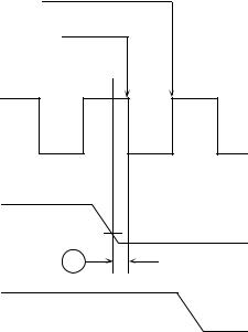
All asynchronous bus arbitration signals to the processor are synchronized before being used internally. As shown in Figure 5-17, synchronization requires a maximum of one cycle of the system clock, assuming that the asynchronous input setup time (#47, defined in Section 10 Electrical Characteristic) has been met. The input asynchronous signal is sampled on the falling edge of the clock and is valid internally after the next falling edge.
MOTOROLA |
M68000 8-/16-/32-BIT MICROPROCESSORS USER'S MANUAL |
5-15 |
INTERNAL SIGNAL VALID
EXTERNAL SIGNAL SAMPLED
CLK
BR (EXTERNAL)
BR (iNTERNAL)
47 |
Figure 5-17. External Asynchronous Signal Synchronization
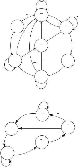
Bus arbitration control is implemented with a finite-state machine. State diagram (a) in Figure 5-18 applies to all processors using 3-wire bus arbitration and state diagram (b) applies to processors using 2-wire bus arbitration, in which BGACK is permanently negated internally or externally. The same finite-state machine is used, but it is effectively a two-state machine because BGACK is always negated.
In Figure 5-18, input signals R and A are the internally synchronized versions of BR and BGACK. The BG output is shown as G, and the internal three-state control signal is shown as T. If T is true, the address, data, and control buses are placed in the high-impedance state when AS is negated. All signals are shown in positive logic (active high), regardless of their true active voltage level. State changes (valid outputs) occur on the next rising edge of the clock after the internal signal is valid.
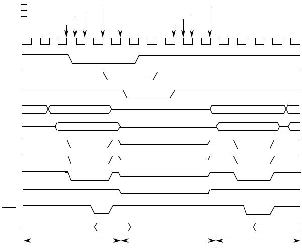
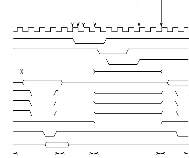
A timing diagram of the bus arbitration sequence during a processor bus cycle is shown in Figure 5-19. The bus arbitration timing while the bus is inactive (e.g., the processor is performing internal operations for a multiply instruction) is shown in Figure 5-20.
When a bus request is made after the MPU has begun a bus cycle and before AS has been asserted (S0), the special sequence shown in Figure 5-21 applies. Instead of being asserted on the next rising edge of clock, BG is delayed until the second rising edge following its internal assertion.
5-16 |
M68000 8-/16-/32-BIT MICROPROCESSORS USER'S MANUAL |
MOTOROLA |
|
|
|
RA |
|
|
|
|
RA |
1 |
GT |
XA |
1 |
RA |
|
|
|
|
|||
|
|
|
|
|
|
|
GT |
|
|
|
RA |
|
GT |
|
|
|
|
|
|
|
|
|
|
RA |
|
|
|
|
RA |
|
|
R+A |
|
|
XX |
|
|
|
|
|
|
|
|
|
|
|
RX |
|
|
|
|
GT |
|
|
|
|
|
|
|
|
|
|
|
XA |
|
|
|
|
|
GT |
|
|
RA |
|
|
GT |
|
|
|
RA |
|
|
|
RA |
|
|
|
|
|
|
|
RA |
|
GT |
XX |
|
|
|
|
|
|
|
|
|
|
|
|
RA |
|
|
|
|
(a) 3-Wire Bus Arbitration |
|||||
|
|
|
R |
|
|
|
|
R |
|
GT |
R |
|
|
|
|
|
STATE 0 |
|
||
|
|
|
|
|
|
|
GT |
|
|
R |
|
|
GT |
|
|
|
|
STATE 4 |
||
STATE 1 |
|
|
|
|
|
|
|
|
|
|
|
|
|
X |
|
|
GT |
|
|
|
|
|
|
X |
|
|
|
|
|
|
STATE 3 |
|
|
|
|
|
|
|
|
|
|
GT |
|
|
|
|
|
|
STATE 2 |
R |
|
|
|
|
|
(b) 2-Wire Bus Arbitration
R
R = Bus Request Internal
A = Bus Grant Acknowledge Internal
G = Bus Grant
T = Three-state Control to Bus Control Logic
X = Don't Care
Notes:
1.State machine will not change if the bus is S0 or S1. Refer to
BUS ARBITRATION CONTROL. 5.2.3.
2.The address bus will be placed in the high-impedance state if T is asserted and AS is negated.
Figure 5-18. Bus Arbitration Unit State Diagrams
Figures 5-19, 5-20, and 5-21 applies to all processors using 3-wire bus arbitration. Figures
5-22, 5-23, and 5-24 applies to all processors using 2-wire bus arbitration.
MOTOROLA |
M68000 8-/16-/32-BIT MICROPROCESSORS USER'S MANUAL |
5-17 |
BUS THREE-STATED |
|
|
|
|
|
|
BUS RELEASED FROM THREE STATE AND |
|
|
|
|
|
|
|
|
|
|
BG ASSERTED |
|
|
|
|
|
|
|
PROCESSOR STARTS NEXT BUS CYCLE |
|
|
|
|
|
|
|
|
|
BR VALID INTERNAL |
|
|
|
|
|
|
BGACK NEGATED INTERNAL |
|
|
|
|
|
|
|
|
|
|
BR SAMPLED |
|
|
|
|
|
|
|
BGACK SAMPLED |
|
|
|
|
|
|
|
|
|
BR ASSERTED |
|
|
|
|
|
|
|
BGACK NEGATED |
|
|
|
|
|
|
|
|
|
CLK |
|
|
|
|
|
|
|
|
|
|
|
|
|
|
|
|
|
S0 |
S1 |
S2 |
S3 |
S4 |
S5 |
S6 |
S7 |
S0 |
S1 |
S2 |
S3 |
S4 |
S5 |
S6 |
S7 |
S0 |
S1 |
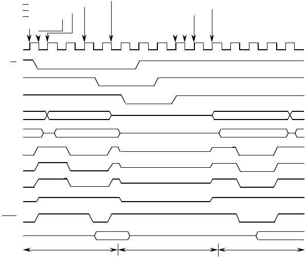
BR
BG
BGACK
FC2–FC0
A23–A1
AS
UDS
LDS
R/W
DTACK
D15–D0
PROCESSOR |
|
ALTERNATE BUS MASTER |
|
PROCESSOR |
Figure 5-19. 3-Wire Bus Arbitration Timing Diagram—Processor Active
5-18 |
M68000 8-/16-/32-BIT MICROPROCESSORS USER'S MANUAL |
MOTOROLA |
BUS RELEASED FROM THREE STATE AND PROCESSOR STARTS NEXT BUS CYCLE  BGACK NEGATED
BG ASSERTED AND BUS THREE STATED  BR VALID INTERNAL
BR SAMPLED 
BR ASSERTED 
CLK
S0 |
S1 |
S2 |
S3 |
S4 |
S5 |
S6 |
S7 |
S0 |
S1 |
S2 |
S3 |
S4 |
BR
BG
BGACK
FC2–FC0
A23–A1
AS
UDS
LDS
R/W
DTACK
D15–D0
|
BUS |
|
|
PROCESSOR |
INACTIVE |
ALTERNATE BUS MASTER |
PROCESSOR |
Figure 5-20. 3-Wire Bus Arbitration Timing Diagram—Bus Inactive
MOTOROLA |
M68000 8-/16-/32-BIT MICROPROCESSORS USER'S MANUAL |
5-19 |
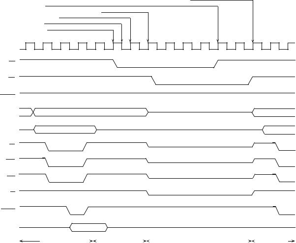
BUS THREE-STATED  BG ASSERTED
BR VALID INTERNAL BR SAMPLED
BR ASSERTED
CLK
BUS RELEASED FROM THREE STATE AND PROCESSOR STARTS NEXT BUS CYCLE  BGACK NEGATED INTERNAL
BGACK SAMPLED 
BGACK NEGATED
S0 |
S2 |
S4 |
S6 |
S0 |
S2 |
S4 |
S6 |
S0 |
BR
BG
BGACK
FC2–FC0
A23–A1
AS
UDS
LDS
R/W
DTACK
D15–D0
PROCESSOR |
|
ALTERNATE BUS MASTER |
|
PROCESSOR |
Figure 5-21. 3-Wire Bus Arbitration Timing Diagram—Special Case
5-20 |
M68000 8-/16-/32-BIT MICROPROCESSORS USER'S MANUAL |
MOTOROLA |
BUS THREE-STATED
BG ASSERTED
BR VALID INTERNAL
BR SAMPLED
BR ASSERTED
CLK
BUS RELEASED FROM THREE STATE AND PROCESSOR STARTS NEXT BUS CYCLE BR NEGATED INTERNAL
BR SAMPLED
BR NEGATED 
S0 |
S1 |
S2 |
S3 |
S4 |
S5 |
S6 |
S7 |
S0 |
S1 |
S2 |
S3 |
S4 |
S5 |
S6 |
S7 |
S0 |
S1 |
BR
BG
BGACK
FC2–FC0
A23–A1
AS
UDS
LDS
R/W
DTACK
D15–D0
 PROCESSOR
 ALTERNATE BUS MASTER
 PROCESSOR
Figure 5-22. 2-Wire Bus Arbitration Timing Diagram—Processor Active
MOTOROLA |
M68000 8-/16-/32-BIT MICROPROCESSORS USER'S MANUAL |
5-21 |
BUS RELEASED FROM THREE STATE AND PROCESSOR STARTS NEXT BUS CYCLE
BR NEGATED
BG ASSERTED AND BUS THREE STATED
BR VALID INTERNAL
BR SAMPLED
BR ASSERTED
CLK
S0 |
S1 |
S2 |
S3 |
S4 |
S5 |
S6 |
S7 |
S0 |
S1 |
S2 |
S3 S4 |
BR
BG
BGACK
FC2–FC0
A23–A1
AS
UDS
LDS
R/W
DTACK
D15–D0
|
|
|
|
|
BUS |
|
|
|
|
|
|
|
|
|
|
PROCESSOR |
|
|
|
|
|
|
|
|
ALTERNATE BUS MASTER |
|
|
|
|
PROCESSOR |
|
|
|
|
|
INACTIVE |
|
|
|
|
|
|
|
|
|||
|
|
|
|
|
|
|
|
|
|
|
|
|
|
|
|
|
|
|
|
|
|
|
|
|
|
|
|
|
|
|
|
Figure 5-23. 2-Wire Bus Arbitration Timing Diagram—Bus Inactive
5-22 |
M68000 8-/16-/32-BIT MICROPROCESSORS USER'S MANUAL |
MOTOROLA |