


10.13 MC68EC000 DC ELECTRICAL SPECIFICATIONS (VCC=5.0 VDC ± 5;PC;
GND=0 VDC; TA = T L TO T H)
|
Characteristic |
|
Input High Voltage |
|
|
Input Low Voltage |
|
|
Input Leakage Current |
BERR, BR, DTACK , CLK, IPL2–IPL0, AVEC |
|
@5.25 V |
|
MODE, HALT, RESET |
Three-State (Off State) Input Current |
AS, A23–A0, D15–D0, |
|
@2.4 V/0.4 V |
|
FC2–FC0, LDS, R/ W, UDS |
Output High Voltage |
|
AS, A23–A0, BG, D15–D0, |
(IOH=–400 A) |
|
FC2–FC0, LDS, R/ W, UDS |
Output Low Voltage |
|
|
(IOL = 1.6 mA) |
|
HALT |
(IOL = 3.2 mA) |
|
A23–A0, BG, FC2–FC0 |
(IOL = 5.0 mA) |
|
RESET |
(IOL = 5.3 mA) |
|
AS, D15–D0, LDS, R/W, UDS |
Current Dissipation* |
|
f=8 MHz |
|
|
f=10 MHz |
|
|
f=12.5 MHz |
|
|
f=16.67 MHz |
|
|
f= 20 MHz |
Power Dissipation |
|
f=8 MHz |
|
|
f=10 MHz |
|
|
f=12.5 MHz |
|
|
f=16.67 MHz |
|
|
f=20 MHz |
Capacitance (Vin=0 V, TA=25°C, Frequency=1 MHz)** |
||
Load Capacitance |
|
HALT |
|
|
All Others |
Symbol |
Min |
Max |
Unit |
VIH |
2.0 |
VCC |
V |
VIL |
GND–0.3 |
0.8 |
V |
Iin |
— |
2.5 |
A |
—20
ITSI — 20 A
VOH |
VCC –0.75 |
— |
V |
VOL |
— |
0.5 |
V |
|
|
||
|
— |
0.5 |
|
|
— |
0.5 |
|
|
— |
0.5 |
|
ID |
— |
25 |
mA |
|
— |
30 |
|
|
— |
35 |
|
|
— |
50 |
|
|
— |
70 |
|
PD |
— |
0.13 |
W |
|
— |
0.16 |
|
|
— |
0.19 |
|
|
— |
0.26 |
|
|
— |
0.38 |
|
Cin |
— |
20.0 |
pF |
CL |
— |
70 |
pF |
|
— |
130 |
|
*Currents listed are with no loading.
**Capacitance is periodically sampled rather than 100% tested.
MOTOROLA |
M68000 8-/16-/32-BIT MICROPROCESSORS USER'S MANUAL |
10-23 |

10.14 MC68EC000 AC ELECTRICAL SPECIFICATIONS — READ AND
WRITE CYCLES (VCC=5.0 VDC ± 5;PC; GND = 0 VDC; TA = TL TO TH; (See Figures 10-12 and 10-13)
Num |
Characteristic |
8 MHz |
10 MHz |
12.5 MHz |
16.67 MHz |
20 MHz |
Unit |
||||||
|
|
Min |
Max |
Min |
Max |
Min |
Max |
Min |
|
Max |
Min |
Max |
|
6 |
Clock Low to Address Valid |
— |
35 |
— |
35 |
— |
35 |
— |
30 |
— |
25 |
|
ns |
6A |
Clock High to FC Valid |
— |
35 |
— |
35 |
— |
35 |
— |
30 |
0 |
25 |
|
ns |
7 |
Clock High to Address, Data Bus |
— |
55 |
— |
55 |
— |
55 |
— |
50 |
— |
42 |
|
ns |
|
High Impedance (Maximum) |
|
|
|
|
|
|
|
|
|
|
|
|
8 |
Clock High to Address, FC Invalid |
0 |
— |
0 |
— |
0 |
— |
0 |
— |
0 |
— |
|
ns |
|
(Minimum) |
|
|
|
|
|
|
|
|
|
|
|
|
91 |
Clock High to AS, DS Asserted |
3 |
35 |
3 |
35 |
3 |
35 |
3 |
|
30 |
3 |
25 |
ns |
112 |
Address Valid to AS, DS Asserted |
30 |
— |
20 |
— |
15 |
— |
15 |
— |
10 |
— |
|
ns |
|
(Read)/AS Asserted (Write) |
|
|
|
|
|
|
|
|
|
|
|
|
11A2 |
FC Valid to AS, DS Asserted |
45 |
— |
45 |
— |
45 |
— |
45 |
— |
40 |
— |
|
ns |
|
(Read)/ AS Asserted (Write) |
|
|
|
|
|
|
|
|
|
|
|
|
121 |
Clock Low to AS, DS Negated |
3 |
35 |
3 |
35 |
3 |
35 |
3 |
|
30 |
3 |
25 |
ns |
132 |
AS, DS Negated to Address, FC |
15 |
— |
15 |
— |
15 |
— |
15 |
— |
10 |
— |
|
ns |
|
Invalid |
|
|
|
|
|
|
|
|
|
|
|
|
142 |
AS (and DS Read) Width |
270 |
— |
195 |
— |
160 |
— |
120 |
— |
100 |
— |
|
ns |
|
Asserted |
|
|
|
|
|
|
|
|
|
|
|
|
14A2 |
DS Width Asserted (Write) |
140 |
— |
95 |
— |
80 |
— |
60 |
— |
50 |
— |
|
ns |
152 |
AS, DS Width Negated |
150 |
— |
105 |
— |
65 |
— |
60 |
— |
50 |
— |
|
ns |
16 |
Clock High to Control Bus High |
— |
55 |
— |
55 |
— |
55 |
— |
50 |
— |
42 |
|
ns |
|
Impedance |
|
|
|
|
|
|
|
|
|
|
|
|
172 |
AS, DS Negated to R/W Invalid |
15 |
— |
15 |
— |
15 |
— |
15 |
— |
10 |
— |
|
ns |
181 |
Clock High to R/W High (Read) |
0 |
35 |
0 |
35 |
0 |
35 |
0 |
|
30 |
0 |
25 |
ns |
201 |
Clock High to R/W Low (Write) |
0 |
35 |
0 |
35 |
0 |
35 |
0 |
|
30 |
0 |
25 |
ns |
20A2,6 |
AS Asserted to R/W Low (Write) |
— |
10 |
— |
10 |
— |
10 |
— |
10 |
— |
10 |
|
ns |
212 |
Address Valid to R/W Low (Write) |
0 |
— |
0 |
— |
0 |
— |
0 |
|
— |
0 |
— |
ns |
21A2 |
FC Valid to R/W Low (Write) |
60 |
— |
50 |
— |
30 |
— |
30 |
— |
25 |
— |
|
ns |
222 |
R/ W Low to DS Asserted (Write) |
80 |
— |
50 |
— |
30 |
— |
30 |
— |
25 |
— |
|
ns |
23 |
Clock Low to Data-Out Valid |
— |
35 |
— |
35 |
— |
35 |
— |
30 |
— |
25 |
|
ns |
|
(Write) |
|
|
|
|
|
|
|
|
|
|
|
|
252 |
AS, DS Negated to Data-Out |
40 |
— |
30 |
— |
20 |
— |
15 |
— |
10 |
— |
|
ns |
|
Invalid (Write) |
|
|
|
|
|
|
|
|
|
|
|
|
262 |
Data-Out Valid to DS Asserted |
40 |
— |
30 |
— |
20 |
— |
15 |
— |
10 |
— |
|
ns |
|
(Write) |
|
|
|
|
|
|
|
|
|
|
|
|
275 |
Data-In Valid to Clock Low (Setup |
5 |
— |
5 |
— |
5 |
— |
5 |
— |
5 |
— |
|
ns |
|
Time on Read) |
|
|
|
|
|
|
|
|
|
|
|
|
282 |
AS, DS Negated to DTACK |
0 |
110 |
0 |
110 |
0 |
110 |
0 |
|
110 |
0 |
95 |
ns |
|
Negated (Asynchronous Hold) |
|
|
|
|
|
|
|
|
|
|
|
|
28A |
Clock High to DTACK Negated |
0 |
110 |
0 |
110 |
0 |
110 |
0 |
|
110 |
0 |
95 |
ns |
10-24 |
M68000 8-/16-/32-BIT MICROPROCESSORS USER'S MANUAL |
MOTOROLA |

Num |
Characteristic |
8 MHz |
10 MHz |
12.5 MHz |
16.67 MHz |
20 MHz |
|
Unit |
||||||
|
|
Min |
Max |
Min |
Max |
Min |
Max |
Min |
Max |
Min |
Max |
|
||
29 |
AS, DS Negated to Data-In Invalid |
0 |
— |
0 |
— |
0 |
— |
0 |
— |
0 |
— |
|
ns |
|
|
(Hold Time on Read) |
|
|
|
|
|
|
|
|
|
|
|
|
|
29A |
AS, DS Negated to Data-In High |
— |
187 |
— |
150 |
— |
120 |
— |
90 |
— |
75 |
|
ns |
|
|
Impedance |
|
|
|
|
|
|
|
|
|
|
|
|
|
30 |
AS, DS Negated to BERR |
0 |
— |
0 |
— |
0 |
— |
0 |
— |
0 |
— |
|
ns |
|
|
Negated |
|
|
|
|
|
|
|
|
|
|
|
|
|
312,5 |
DTACK Asserted to Data-In Valid |
— |
90 |
— |
65 |
— |
50 |
— |
50 |
— |
42 |
|
ns |
|
|
(Setup Time) |
|
|
|
|
|
|
|
|
|
|
|
|
|
32 |
HALT and RESET Input Transition |
0 |
150 |
0 |
150 |
0 |
150 |
0 |
|
150 |
0 |
150 |
ns |
|
|
Time |
|
|
|
|
|
|
|
|
|
|
|
|
|
33 |
Clock High to BG Asserted |
— |
35 |
— |
35 |
— |
35 |
0 |
30 |
0 |
25 |
ns |
||
34 |
Clock High to BG Negated |
— |
35 |
— |
35 |
— |
35 |
0 |
30 |
0 |
25 |
ns |
||
35 |
BR Asserted to BG Asserted |
1.5 |
3.5 |
1.5 |
3.5 |
1.5 |
3.5 |
1.5 |
|
3.5 |
1.5 |
3.5 |
|
Clks |
367 |
BR Negated to BG Negated |
1.5 |
3.5 |
1.5 |
3.5 |
1.5 |
3.5 |
1.5 |
|
3.5 |
1.5 |
3.5 |
|
Clks |
38 |
BG Asserted to Control, Address, |
— |
55 |
— |
55 |
— |
55 |
— |
50 |
— |
42 |
|
ns |
|
|
Data Bus High Impedance (AS |
|
|
|
|
|
|
|
|
|
|
|
|
|
|
Negated) |
|
|
|
|
|
|
|
|
|
|
|
|
|
39 |
BG Width Negated |
1.5 |
|
1.5 |
|
1.5 |
|
1.5 |
|
|
1.5 |
— |
|
Clks |
44 |
AS, DS Negated to VPA Negated |
0 |
55 |
0 |
55 |
0 |
55 |
0 |
|
50 |
0 |
42 |
|
ns |
475 |
Asynchronous Input Setup Time |
5 |
— |
5 |
— |
5 |
— |
5 |
|
— |
5 |
— |
|
ns |
482,3 |
BERR Asserted to DTACK |
20 |
— |
20 |
— |
20 |
— |
10 |
— |
10 |
— |
|
ns |
|
|
Asserted |
|
|
|
|
|
|
|
|
|
|
|
|
|
53 |
Data-Out Hold from Clock High |
0 |
— |
0 |
— |
0 |
— |
0 |
|
— |
0 |
— |
|
ns |
55 |
R/ W Asserted to Data Bus |
30 |
— |
20 |
— |
10 |
— |
0 |
— |
0 |
— |
|
ns |
|
|
Impedance Change |
|
|
|
|
|
|
|
|
|
|
|
|
|
564 |
HALT/RESET Pulse Width |
10 |
— |
10 |
— |
10 |
— |
10 |
— |
10 |
— |
|
|
Clks |
587 |
BR Negated to AS, DS, R/W |
1.5 |
— |
1.5 |
— |
1.5 |
— |
1.5 |
— |
1.5 |
— |
Clks |
||
|
Driven |
|
|
|
|
|
|
|
|
|
|
|
|
|
58A7 |
BR Negated to FC, VMA Driven |
1 |
— |
1 |
— |
1 |
— |
1 |
— |
1 |
— |
|
|
Clks |
NOTES:1. For a loading capacitance of less than or equal to 50 pF, subtract 5 ns from the value given in the maximum columns.
2. Actual value depends on clock period.
3.I f #47 is satisfied for both DTACK and BERR, #48 may be ignored. In the absence of DTACK, BERR is an asynchronous input using the asynchronous input setup time (#47).
4.For power-up, the MC68EC000 must be held in the reset state for 520 clocks to allow stabilization of onchip circuitry. After the system is powered up, #56 refers to the minimum pulse width required to
reset the processor.
5.If the asynchronous input setup time (#47) requirement is satisfied for DTACK, the DTACK-asserted to data setup time (#31) requirement can be ignored. The data must only satisfy the data-in to clock low
setup time (#27) for the following clock cycle.
6.When AS and R/W are equally loaded (±20;pc), subtract 5 ns from the values given in these columns.
7.The minimum value must be met to guarantee proper operation. If the maximum value is exceeded,
BG may be reasserted.
8. DS is used in this specification to indicate UDS and LDS.
MOTOROLA |
M68000 8-/16-/32-BIT MICROPROCESSORS USER'S MANUAL |
10-25 |
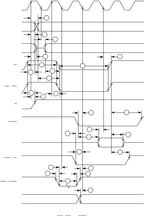
CLK
FC2–FC0
A23–A0
AS
LDS / UDS
R/W
DTACK
DATA IN
BERR / BR (NOTE 2)
HALT / RESET
ASYNCHRONOUS INPUTS (NOTE 1)
S0 |
S1 |
S2 |
S3 |
S4 |
S5 |
S6 |
S7 |
|
6A |
|
|
|
|
|
|
|
8 |
|
|
|
|
|
|
|
|
6 |
|
|
|
|
|
|
7 |
|
|
|
|
|
12 |
|
15 |
|
|
|
14 |
|
|
|
|
|
|
|
|
|
|
13 |
|
11 |
|
|
|
|
|
|
|
|
|
|
|
|
|
|
11A |
|
|
|
|
|
|
17 |
18 |
9 |
|
|
|
|
|
|
|
|
|
|
|
|
|
|
|
|
|
|
47 |
|
28 |
|
|
|
|
|
27 |
|
|
|
|
|
48 |
|
31 |
|
29 |
|
|
|
|
|
|
||
|
|
|
|
|
|
|
|
|
|
|
|
|
47 |
|
30 |
|
|
47 |
|
|
47 |
|
|
|
|
|
|
|
|
|
|
|
32 |
|
|
|
32 |
|
|
|
|
|
56 |
|
|
|
|
|
|
|
|
|
47 |
|
|
NOTES:
1.Setup time for the asynchronous inputs IPL2–IPL0 and AVEC (#47) guarantees their recognition at the next falling edge of the clock.
2.BR need fall at this time only to insure being recognized at the end of the bus cycle.
3.Timing measurements are referenced to and from a low voltage of 0.8 V and a high voltage of 2.0 V, unless otherwise noted. The voltage swing through this range should start outside and pass through the range such that the rise or fall is linear between 0.8 V and 2.0 V.
Figure 10-12. MC68EC000 Read Cycle Timing Diagram
10-26 |
M68000 8-/16-/32-BIT MICROPROCESSORS USER'S MANUAL |
MOTOROLA |
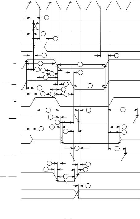
CLK
FC2-FC0
A23-A0
AS
LDS / UDS
R/W
DTACK
DATA OUT
BERR / BR (NOTE 2)
HALT / RESET
ASYNCHRONOUS INPUTS (NOTE 1)
S0 |
|
S1 |
S2 |
S3 |
S4 |
S5 |
S6 |
S7 |
|
|
|
6A |
|
|
|
|
|
|
|
8 |
|
|
|
|
|
|
|
|
|
6 |
|
|
|
|
|
|
|
7 |
|
|
|
|
|
12 |
|
|
15 |
|
|
|
14 |
|
|
|
|
|
|
|
|
|
|
|
|
13 |
9 |
|
|
|
9 |
|
|
|
|
11 |
|
|
|
|
||
|
|
|
|
|
|
|
||
|
|
|
|
|
|
|
|
|
|
|
11A |
|
|
|
|
|
|
|
|
|
|
20A |
|
14A |
|
|
|
17 |
|
|
|
|
|
||
|
|
20 |
|
|
|
|
||
|
|
|
|
|
|
|
|
|
|
|
18 |
21 |
22 |
|
|
|
|
|
|
|
21A |
|
|
47 |
|
28 |
|
|
|
55 |
|
|
|
|
|
|
|
|
26 |
|
|
|
|
|
|
|
7 |
23 |
|
|
|
|
53 |
|
|
|
48 |
|
|
|
25 |
|
|
|
|
|
|
|
|
||
|
|
|
|
|
47 |
|
|
30 |
|
|
|
47 |
|
|
47 |
|
|
|
|
|
|
|
|
|
|
|
|
|
32 |
|
|
32 |
|
|
|
|
|
|
|
56 |
|
|
|
|
|
|
|
|
|
|
47 |
|
|
NOTES:
1. Timing measurements are referenced to and from a low voltage of 0.8 V and a high voltage of 2.0 V, unless otherwise noted. The voltage swing through this range should start outside and pass through the range such that the rise or fall is linear between 0.8 V and 2.0 V.
2. Because of loading variations, R/W may be valid after AS even though both are initiated by the rising edge of S2 (specification #20A).
Figure 10-13. MC68EC000 Write Cycle Timing Diagram
MOTOROLA |
M68000 8-/16-/32-BIT MICROPROCESSORS USER'S MANUAL |
10-27 |

10.15MC68EC000 AC ELECTRICAL SPECIFICATIONS—BUS
ARBITRATION (VCC=5.0VDC ± 5%; GND=0 VDC; TA = TL TO TH; see Figure 10-14)
Num |
Characteristic |
8 MHz |
10 MHz |
12.5 MHz |
16.67 MHz |
|
20 MHz |
Unit |
|||||
|
|
Min |
Max |
Min |
Max |
Min |
Max |
Min |
Max |
Min Max |
|
||
7 |
Clock High to Address, Data |
— |
55 |
— |
55 |
— |
55 |
— |
50 |
— |
42 |
ns |
|
|
Bus High Impedance |
|
|
|
|
|
|
|
|
|
|
|
|
|
(Maximum) |
|
|
|
|
|
|
|
|
|
|
|
|
16 |
Clock High to Control Bus High |
— |
55 |
— |
55 |
— |
55 |
— |
50 |
— |
42 |
ns |
|
|
Impedance |
|
|
|
|
|
|
|
|
|
|
|
|
33 |
Clock High to BG Asserted |
— |
35 |
— |
35 |
— |
35 |
0 |
30 |
0 |
25 |
ns |
|
34 |
Clock High to BG Negated |
— |
35 |
— |
35 |
— |
35 |
0 |
30 |
0 |
25 |
ns |
|
35 |
BR Asserted to BG Asserted |
1.5 |
3.5 |
1.5 |
3.5 |
1.5 |
3.5 |
1.5 |
3.5 |
|
1.5 |
3.5 |
Clks |
367 |
BR Negated to BG Negated |
1.5 |
3.5 |
1.5 |
3.5 |
1.5 |
3.5 |
1.5 |
3.5 |
|
1.5 |
3.5 |
Clks |
38 |
BG Asserted to Control, |
— |
55 |
— |
55 |
— |
55 |
— |
50 |
— |
42 |
ns |
|
|
Address, Data Bus High |
|
|
|
|
|
|
|
|
|
|
|
|
|
Impedance (AS Negated) |
|
|
|
|
|
|
|
|
|
|
|
|
39 |
BG Width Negated |
1.5 |
— |
1.5 |
— |
1.5 |
— |
1.5 |
— |
1.5 |
— |
|
Clks |
47 |
Asynchronous Input Setup |
5 |
— |
5 |
— |
5 |
— |
5 |
— |
5 |
— |
ns |
|
|
Time |
|
|
|
|
|
|
|
|
|
|
|
|
581 |
BR Negated to AS, DS, R/W |
1.5 |
— |
1.5 |
— |
1.5 |
— |
1.5 |
— |
1.5 |
— |
Clks |
|
|
Driven |
|
|
|
|
|
|
|
|
|
|
|
|
58A1 |
BR Negated to FC Driven |
1 |
— |
1 |
— |
1 |
— |
1 |
— |
1 |
— |
|
Clks |
NOTES: 1.The minimum value must be met to guarantee proper operation. If the maximum value is exceeded, BG may be reasserted.
2.DS is used in this specification to indicate UDS and LDS.
10-28 |
M68000 8-/16-/32-BIT MICROPROCESSORS USER'S MANUAL |
MOTOROLA |
CLK |
|
|
47 |
|
|
33 |
|
|
BR |
34 |
|
35 |
36 |
|
BG |
|
|
39 |
58 |
|
38 |
||
|
||
AS |
|
|
DS |
|
|
R/W |
|
|
|
58A |
|
FC2-FC0 |
|
|
A19-A0 |
|
|
D7-D0 |
|
|
NOTES: Waveform measurements for all inputs and outputs are specified at: logic high 2.0 V, logic low = 0.8 V. |
|
Figure 10-14. MC68EC000 Bus Arbitration Timing Diagram
MOTOROLA |
M68000 8-/16-/32-BIT MICROPROCESSORS USER'S MANUAL |
10-29 |