

SECTION 8
16-BIT INSTRUCTION EXECUTION TIMES
This section contains listings of the instruction execution times in terms of external clock
(CLK) periods for the MC68000, MC68HC000, MC68HC001, and the MC68EC000 in 16bit mode. In this data, it is assumed that both memory read and write cycles consist of four clock periods. A longer memory cycle causes the generation of wait states that must be added to the total instruction times.
The number of bus read and write cycles for each instruction is also included with the timing data. This data is shown as
n(r/w)
where:
n is the total number of clock periods
r is the number of read cycles
w is the number of write cycles
For example, a timing number shown as 18(3/1) means that the total number of clock periods is 18. Of the 18 clock periods, 12 are used for the three read cycles (four periods per cycle). Four additional clock periods are used for the single write cycle, for a total of 16 clock periods. The bus is idle for two clock periods during which the processor completes the internal operations required for the instruction.
NOTE
The total number of clock periods (n) includes instruction fetch and all applicable operand fetches and stores.
8.1 OPERAND EFFECTIVE ADDRESS CALCULATION TIMES
Table 8-1 lists the numbers of clock periods required to compute the effective addresses for instructions. The total includes fetching any extension words, computing the address, and fetching the memory operand. The total number of clock periods, the number of read cycles, and the number of write cycles (zero for all effective address calculations) are shown in the previously described format.
MOTOROLA |
MC68000 8-/16-/32-MICROPROCESSORS USER’S MANUAL |
8-1 |

Table 8-1. Effective Address Calculation Times
|
Addressing Mode |
Byte, Word |
Long |
|
Register |
|
|
Dn |
Data Register Direct |
0(0/0) |
0(0/0) |
An |
Address Register Direct |
0(0/0) |
0(0/0) |
|
Memory |
|
|
(An) |
Address Register Indirect |
4(1/0) |
8(2/0) |
(An)+ |
Address Register Indirect with Postincrement |
4(1/0) |
8(2/0) |
–(An) |
Address Register Indirect with Predecrement |
6(1/0) |
10(2/0) |
(d 16, An) |
Address Register Indirect with Displacement |
8(2/0) |
12(3/0) |
(d 8, An, Xn)* |
Address Register Indirect with Index |
10(2/0) |
14(3/0) |
(xxx).W |
Absolute Short |
8(2/0) |
12(3/0) |
(xxx).L |
Absolute Long |
12(3/0) |
16(4/0) |
(d 8, PC) |
Program Counter Indirect with Displacement |
8(2/0) |
12(3/0) |
(d 16, PC, Xn)* |
Program Counter Indirect with Index |
10(2/0) |
14(3/0) |
#<data> |
Immediate |
4(1/0) |
8(2/0) |
*The size of the index register (Xn) does not affect execution time.
8.2 MOVE INSTRUCTION EXECUTION TIMES
Tables 8-2 and 8-3 list the numbers of clock periods for the move instructions. The totals include instruction fetch, operand reads, and operand writes. The total number of clock periods, the number of read cycles, and the number of write cycles are shown in the previously described format.
Table 8-2. Move Byte and Word Instruction Execution Times
|
|
|
|
|
Destination |
|
|
|
|
Source |
Dn |
An |
(An) |
(An)+ |
–(An) |
(d16, An) |
(d8, An, Xn)* |
(xxx).W |
(xxx).L |
Dn |
4(1/0) |
4(1/0) |
8(1/1) |
8(1/1) |
8(1/1) |
12(2/1) |
14(2/1) |
12(2/1) |
16(3/1) |
An |
4(1/0) |
4(1/0) |
8(1/1) |
8(1/1) |
8(1/1) |
12(2/1) |
14(2/1) |
12(2/1) |
16(3/1) |
(An) |
8(2/0) |
8(2/0) |
12(2/1) |
12(2/1) |
12(2/1) |
16(3/1) |
18(3/1) |
16(3/1) |
20(4/1) |
(An)+ |
8(2/0) |
8(2/0) |
12(2/1) |
12(2/1) |
12(2/1) |
16(3/1) |
18(3/1) |
16(3/1) |
20(4/1) |
–(An) |
10(2/0) |
10(2/0) |
14(2/1) |
14(2/1) |
14(2/1) |
18(3/1) |
20(3/1) |
18(3/1) |
22(4/1) |
(d 16, An) |
12(3/0) |
12(3/0) |
16(3/1) |
16(3/1) |
16(3/1) |
20(4/1) |
22(4/1) |
20(4/1) |
24(5/1) |
(d 8, An, Xn)* |
14(3/0) |
14(3/0) |
18(3/1) |
18(3/1) |
18(3/1) |
22(4/1) |
24(4/1) |
22(4/1) |
26(5/1) |
(xxx).W |
12(3/0) |
12(3/0) |
16(3/1) |
16(3/1) |
16(3/1) |
20(4/1) |
22(4/1) |
20(4/1) |
24(5/1) |
(xxx).L |
16(4/0) |
16(4/0) |
20(4/1) |
20(4/1) |
20(4/1) |
24(5/1) |
26(5/1) |
24(5/1) |
28(6/1) |
(d 16, PC) |
12(3/0) |
12(3/0) |
16(3/1) |
16(3/1) |
16(3/1) |
20(4/1) |
22(4/1) |
20(4/1) |
24(5/1) |
(d 8, PC, Xn)* |
14(3/0) |
14(3/0) |
18(3/1) |
18(3/1) |
18(3/1) |
22(4/1) |
24(4/1) |
22(4/1) |
26(5/1) |
#<data> |
8(2/0) |
8(2/0) |
12(2/1) |
12(2/1) |
12(2/1) |
16(3/1) |
18(3/1) |
16(3/1) |
20(4/1) |
*The size of the index register (Xn) does not affect execution time.
8-2 |
MC68000 8-/16-/32-MICROPROCESSORS UISER'S MANUAL |
MOTOROLA |

Table 8-3. Move Long Instruction Execution Times
|
|
|
|
|
Destination |
|
|
|
|
Source |
Dn |
An |
(An) |
(An)+ |
–(An) |
(d16, An) |
(d8, An, Xn)* |
(xxx).W |
(xxx).L |
Dn |
4(1/0) |
4(1/0) |
12(1/2) |
12(1/2) |
12(1/2) |
16(2/2) |
18(2/2) |
16(2/2) |
20(3/2) |
An |
4(1/0) |
4(1/0) |
12(1/2) |
12(1/2) |
12(1/2) |
16(2/2) |
18(2/2) |
16(2/2) |
20(3/2) |
(An) |
12(3/0) |
12(3/0) |
20(3/2) |
20(3/2) |
20(3/2) |
24(4/2) |
26(4/2) |
24(4/2) |
28(5/2) |
(An)+ |
12(3/0) |
12(3/0) |
20(3/2) |
20(3/2) |
20(3/2) |
24(4/2) |
26(4/2) |
24(4/2) |
28(5/2) |
–(An) |
14(3/0) |
14(3/0) |
22(3/2) |
22(3/2) |
22(3/2) |
26(4/2) |
28(4/2) |
26(4/2) |
30(5/2) |
(d 16, An) |
16(4/0) |
16(4/0) |
24(4/2) |
24(4/2) |
24(4/2) |
28(5/2) |
30(5/2) |
28(5/2) |
32(6/2) |
(d 8, An, Xn)* |
18(4/0) |
18(4/0) |
26(4/2) |
26(4/2) |
26(4/2) |
30(5/2) |
32(5/2) |
30(5/2) |
34(6/2) |
(xxx).W |
16(4/0) |
16(4/0) |
24(4/2) |
24(4/2) |
24(4/2) |
28(5/2) |
30(5/2) |
28(5/2) |
32(6/2) |
(xxx).L |
20(5/0) |
20(5/0) |
28(5/2) |
28(5/2) |
28(5/2) |
32(6/2) |
34(6/2) |
32(6/2) |
36(7/2) |
(d, PC) |
16(4/0) |
16(4/0) |
24(4/2) |
24(4/2) |
24(4/2) |
28(5/2) |
30(5/2) |
28(5/2) |
32(5/2) |
(d, PC, Xn)* |
18(4/0) |
18(4/0) |
26(4/2) |
26(4/2) |
26(4/2) |
30(5/2) |
32(5/2) |
30(5/2) |
34(6/2) |
#<data> |
12(3/0) |
12(3/0) |
20(3/2) |
20(3/2) |
20(3/2) |
24(4/2) |
26(4/2) |
24(4/2) |
28(5/2) |
*The size of the index register (Xn) does not affect execution time.
8.3 STANDARD INSTRUCTION EXECUTION TIMES
The numbers of clock periods shown in Table 8-4 indicate the times required to perform the operations, store the results, and read the next instruction. The total number of clock periods, the number of read cycles, and the number of write cycles are shown in the previously described format. The number of clock periods, the number of read cycles, and the number of write cycles, respectively, must be added to those of the effective address calculation where indicated by a plus sign (+).
In Table 8-4, the following notation applies:
An — Address register operand Dn — Data register operand
ea — An operand specified by an effective address M — Memory effective address operand
MOTOROLA |
MC68000 8-/16-/32-MICROPROCESSORS USER’S MANUAL |
8-3 |
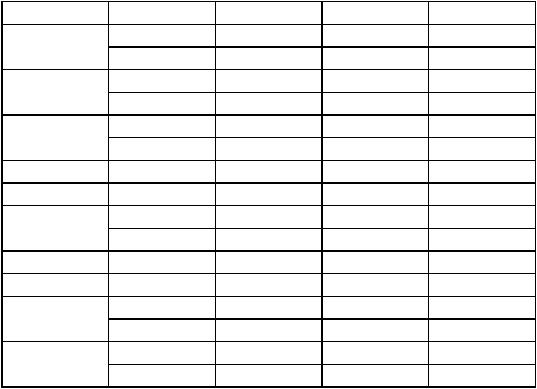
Table 8-4. Standard Instruction Execution Times
Instruction |
Size |
op<ea>, An† |
op<ea>, Dn |
op Dn, <M> |
ADD/ADDA |
Byte, Word |
8(1/0)+ |
4(1/0)+ |
8(1/1)+ |
|
Long |
6(1/0)+** |
6(1/0)+** |
12(1/2)+ |
AND |
Byte, Word |
— |
4(1/0)+ |
8(1/1)+ |
|
Long |
— |
6(1/0)+** |
12(1/2)+ |
CMP/CMPA |
Byte, Word |
6(1/0)+ |
4(1/0)+ |
— |
|
Long |
6(1/0)+ |
6(1/0)+ |
— |
DIVS |
— |
— |
158(1/0)+* |
— |
DIVU |
— |
— |
140(1/0)+* |
— |
EOR |
Byte, Word |
— |
4(1/0)*** |
8(1/1)+ |
|
Long |
— |
8(1/0)*** |
12(1/2)+ |
MULS |
— |
— |
70(1/0)+* |
— |
MULU |
— |
— |
70(1/0)+* |
— |
OR |
Byte, Word |
— |
4(1/0)+ |
8(1/1)+ |
|
Long |
— |
6(1/0)+** |
12(1/2)+ |
SUB |
Byte, Word |
8(1/0)+ |
4(1/0)+ |
8(1/1)+ |
|
Long |
6(1/0)+** |
6(1/0)+** |
12(1/2)+ |
+ Add effective address calculation time.
†Word or long only
*Indicates maximum basic value added to word effective address time
**The base time of six clock periods is increased to eight if the effective address mode is register direct or immediate (effective address time should also be added).
***Only available effective address mode is data register direct.
DIVS, DIVU — The divide algorithm used by the MC68000 provides less than 10% difference between the bestand worst-case timings.
MULS, MULU — The multiply algorithm requires 38+2n clocks where n is defined as: MULU: n = the number of ones in the <ea>
MULS: n=concatenate the <ea> with a zero as the LSB; n is the resultant number of 10
or 01 patterns in the 17-bit source; i.e., worst case happens when the source is $5555.
8.4 IMMEDIATE INSTRUCTION EXECUTION TIMES
The numbers of clock periods shown in Table 8-5 include the times to fetch immediate operands, perform the operations, store the results, and read the next operation. The total number of clock periods, the number of read cycles, and the number of write cycles are shown in the previously described format. The number of clock periods, the number of read cycles, and the number of write cycles, respectively, must be added to those of the effective address calculation where indicated by a plus sign (+).
In Table 8-5, the following notation applies:
# — Immediate operand
Dn — Data register operand An — Address register operand
M — Memory operand
8-4 |
MC68000 8-/16-/32-MICROPROCESSORS UISER'S MANUAL |
MOTOROLA |