

SECTION 10
ELECTRICAL AND THERMAL CHARACTERISTICS
This section provides information on the maximum rating and thermal characteristics for the MC68000, MC68HC000, MC68HC001, MC68EC000, MC68008, and MC68010.
10.1 MAXIMUM RATINGS
Rating |
Symbol |
Value |
Unit |
Supply Voltage |
VCC |
–0.3 to 7.0 |
V |
Input Voltage |
Vin |
–0.3 to 7.0 |
V |
Maximum Operating |
TA |
TL to TH |
°C |
Temperature Range |
|
0 to 70 |
|
Commerical Extended "C" Grade |
|
–40 to 85 |
|
Commerical Extended "I" Grade |
|
0 to 85 |
|
Storage Temperature |
Tstg |
–55 to 150 |
°C |
10.2 THERMAL CHARACTERISTICS
This device contains protective circuitry against damage due to high static voltages or electrical fields; however, it is advised that normal precautions be taken to avoid application of any voltages higher than maximum-rated voltages to this high-impedance circuit. Reliability of operation is enhanced if unused inputs are tied to an appropriate logic voltage level (e.g., either GND or V CC ).
Characteristic |
Symbol Value |
Symbol |
Value Rating |
Thermal Resistance |
θJA |
θJC |
°C/W |
Ceramic, Type L/LC |
30 |
|
15* |
Ceramic, Type R/RC |
33 |
|
15 |
Plastic, Type P |
30 |
|
15* |
Plastic, Type FN |
45* |
|
25* |
*Estimated
MOTOROLA |
M68000 8-/16-/32-BIT MICROPROCESSORS USER'S MANUAL |
10-1 |
10.3 POWER CONSIDERATIONS
The average die-junction temperature, TJ, in °C can be obtained from:
T = T |
+(P |
• θJ ) |
(1) |
|
J |
A |
D |
A |
|
where: |
|
|
|
|
TA |
= |
Ambient Temperature, °C |
|
|
θJA |
= Package Thermal Resistance, Junction-to-Ambient, °C/W |
|
||
PD |
= |
PINT + PI/O |
|
|
PINT |
= |
ICC x VCC, Watts — Chip Internal Power |
|
|
PI/O |
= Power Dissipation on Input and Output Pins — User Determined |
|
||
For most applications, PI/O<PINT and can be neglected.
An appropriate relationship between PD and TJ (if PI/O is neglected) is: |
|
PD = K (TJ + 273 °C) |
(2) |
Solving Equations (1) and (2) for K gives: |
|
K = PD • (TA + 273°C) + θJA • P D2 |
(3) |
where K is a constant pertaining to the particular part. K can be determined from equation
(3) by measuring PD (at thermal equilibrium) for a known TA. Using this value of K, the values of PD and TJ can be obtained by solving Equations (1) and (2) iteratively for any value of TA.
The curve shown in Figure 10-1 gives the graphic solution to the above equations for the specified power dissipation of 1.5 W over the ambient temperature range of -55 °C to 125 °C using a maximum θ JA of 45 °C/W. Ambient temperature is that of the still air surrounding the device. Lower values of θJA cause the curve to shift downward slightly; for instance, for θJA of 40 °/W, the curve is just below 1.4 W at 25 °C.
The total thermal resistance of a package (θ JA) can be separated into two components,
θJC and θCA, representing the barrier to heat flow from the semiconductor junction to the package (case) surface (θJC) and from the case to the outside ambient air (θ CA). These terms are related by the equation:
θJA = θJC + θCA |
(4) |
θJC is device related and cannot be influenced by the user. However, θ CA is user dependent and can be minimized by such thermal management techniques as heat sinks, ambient air cooling, and thermal convection. Thus, good thermal management on the part of the user can significantly reduce θCA so that θ JA approximately equals ;θJC. Substitution of θJC for θ JA in equation 1 results in a lower semiconductor junction temperature.
10-2 |
M68000 8-/16-/32-BIT MICROPROCESSORS USER'S MANUAL |
MOTOROLA |
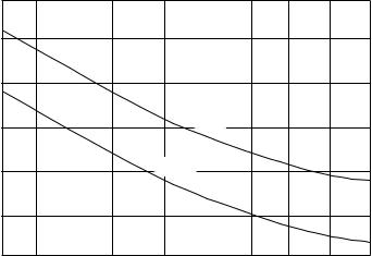
Table 10-1 summarizes maximum power dissipation and average junction temperature for the curve drawn in Figure 10-1, using the minimum and maximum values of ambient temperature for different packages and substituting θJC for θ JA (assuming good thermal management). Table 10-2 provides the maximum power dissipation and average junction temperature assuming that no thermal management is applied (i.e., still air).
NOTE
Since the power dissipation curve shown in Figure 10-1 is negatively sloped, power dissipation declines as ambient temperature increases. Therefore, maximum power dissipation occurs at the lowest rated ambient temperature, but the highest average junction temperature occurs at the maximum ambient temperature where power dissipation is lowest.
POWER (PD ), WATTS
2.2
2.0
1.8
|
16. |
|
1.6 |
67 |
MHz |
|
|
|
|
8, |
10, 12. |
|
|
|
|
1.4 |
|
|
|
|
|
|
|
|
|
|
|
5 |
MHz |
|
|
|
|
|
|
|
|
|
|
|
|
|
1.2 |
|
|
|
|
|
|
|
|
1.0 |
|
|
|
|
|
|
|
|
- 55 |
- 40 |
0 |
|
25 |
70 |
85 |
110 |
125 |
AMBIENT TEMPERATURE (TA ), C
C
Figure 10-1. MC68000 Power Dissipation (PD) vs Ambient Temperature (TA) (Not Applicable to MC68HC000/68HC001/68EC000)
MOTOROLA |
M68000 8-/16-/32-BIT MICROPROCESSORS USER'S MANUAL |
10-3 |

Table 10-1. Power Dissipation and Junction Temperature vs Temperature (θJC=θJA)
Package |
T Range |
θJ |
P (W) |
T (°C) |
P (W) |
T (°C) |
|
A |
C |
D |
J |
D |
J |
|
|
(°C/W) |
@ T A Min. |
@ T A Min. |
@ T A Max. |
@ T A Max. |
L/LC |
0°C to 70°C |
15 |
1.5 |
23 |
1.2 |
88 |
|
-40°C to 85°C |
15 |
1.7 |
-14 |
1.2 |
103 |
|
0°C to 85°C |
15 |
1.5 |
23 |
1.2 |
103 |
P |
0°C to 70°C |
15 |
1.5 |
23 |
1.2 |
88 |
R/RC |
0°C to 70°C |
15 |
1.5 |
23 |
1.2 |
88 |
|
-40°C to 85°C |
15 |
1.7 |
-14 |
1.2 |
103 |
|
0°C to 85°C |
15 |
1.5 |
23 |
1.2 |
103 |
FN |
0°C to 70°C |
25 |
1.5 |
38 |
1.2 |
101 |
NOTE: Table does not include values for the MC68000 12F.
Does not apply to the MC68HC000, MC68HC001, and MC68EC000.
Table 10-2. Power Dissipation and Junction Temperature vs Temperature (θJC≠θJC)
Package |
T Range |
θJ |
P (W) |
T (°C) |
P (W) |
T (°C) |
|
A |
A |
D |
J |
D |
J |
|
|
(°C/W) |
@ T A Min. |
@ T A Min. |
@ T A Max. |
@ T A Max. |
L/LC |
0°C to 70°C |
30 |
1.5 |
23 |
1.2 |
88 |
|
-40°C to 85°C |
30 |
1.7 |
-14 |
1.2 |
103 |
|
0°C to 85°C |
30 |
1.5 |
23 |
1.2 |
103 |
P |
0°C to 70°C |
30 |
1.5 |
23 |
1.2 |
88 |
R/RC |
0°C to 70°C |
33 |
1.5 |
23 |
1.2 |
88 |
|
-40°C to 85°C |
33 |
1.7 |
-14 |
1.2 |
103 |
|
0°C to 85°C |
33 |
1.5 |
23 |
1.2 |
103 |
FN |
0°C to 70°C |
40 |
1.5 |
38 |
1.2 |
101 |
NOTE: Table does not include values for the MC68000 12F.
Does not apply to the MC68HC000, MC68HC001, and MC68EC000.
Values for thermal resistance presented in this manual, unless estimated, were derived using the procedure described in Motorola Reliability Report 7843 “Thermal Resistance
Measurement Method for MC68XXX Microcomponent Devices”’ and are provided for design purposes only. Thermal measurements are complex and dependent on procedure and setup. User-derived values for thermal resistance may differ.
10.4 CMOS CONSIDERATIONS
The MC68HC000, MC68HC001, and MC68EC000, with it significantly lower power consumption, has other considerations. The CMOS cell is basically composed of two complementary transistors (a P channel and an N channel), and only one transistor is turned on while the cell is in the steady state. The active P-channel transistor sources current when the output is a logic high and presents a high impedance when the output is logic low. Thus, the overall result is extremely low power consumption because no power
10-4 |
M68000 8-/16-/32-BIT MICROPROCESSORS USER'S MANUAL |
MOTOROLA |